ESMT
M23L416256A
Elite Semiconductor Memory Technology Inc.
Publication Date : Mar. 2003
Revision : 1.0
1/12
SRAM
256K x 16 Bit
SUPER LOW POWER/VOLTAGE CMOS SRAM
Features
Operating voltage: 2.7V to 3.6V
Access times: 55 / 70 ns (max.)
Wide operating temperature range :
- Industrial grade : -40
�
C to + 85
�
C
Full static operation, no clock or refreshing required
All inputs and outputs are directly TTL-compatible
Common I/O using three-state output
Data retention voltage: 1.5V (min.)
Available in 48-ball 6x8mm Mini-BGA packages
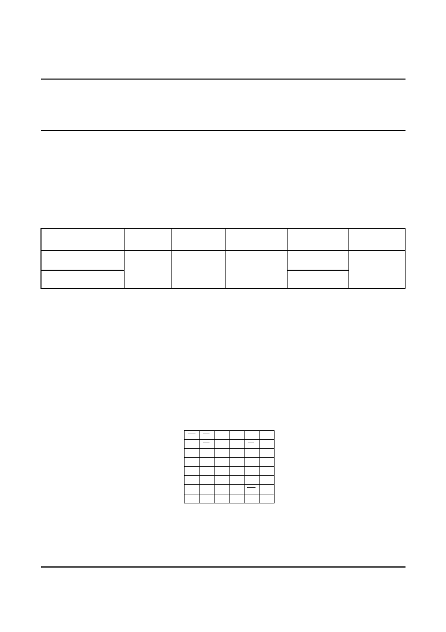
Ordering Information
44-pin 400mil TSOP ( Type II )
48-ball 6x8mm Mini-BGA
Product No.
Operating
Voltage
Operating
Temperature
Operating Current
Icc1 (max.)
Standby Current
Isb1 ( max.)
Packing Type
M23L416256A � 55 SB
*1
M23L416256A � 70 SB
*1
10 uA
M23L416256A � 55 LB
*1
M23L416256A � 70 LB
*1
+2.7V ~ +3.6V
-40
�
C ~ +85
�
C
45 mA
40 uA
6 x 8 mm Mini-BGA
Notes *1 : S means Super Low Power , L means Low Power.
General Description
The M23L416256A is a low operating current 4,194,304-
bit static random access memory organized as 262,144
words by 16 bits and operates on low power voltage from
2.7V to 3.6V. It is built using high performance CMOS
process.
Inputs and three-state outputs are TTL compatible and
allow for direct interfacing with common system bus
structures.
The chip enable input is provided for POWER-DOWN,
device enable. Two byte enable inputs and an output
enable input are included for easy interfacing.
Data retention is guaranteed at a power supply voltage as
low as 1.5V.
Pin Configurations
Mini-BGA 48-ball Top View
I/O
9
I/O
10
GND
VCC
I/O
15
I/O
16
NC
A8
NC
A9
A12
A10
A11
NC
A13
A14
A15
I/O
8
I/O
7
I/O
3
I/O
1
GND
VCC
A0
A3
A5
A6
A4
A1
A2
NC
6
5
4
3
2
1
A
B
C
D
E
F
G
H
I/O
14
I/O
13
I/O
12
I/O
11
A17
NC
A7
A16
I/O
2
I/O
4
I/O
5
I/O
6
LB
HB
WE
OE
CE
ESMT
Preliminary M23L416256A
Elite Semiconductor Memory Technology Inc.
Publication Date : Mar. 2003
Revision : 1.0
2/12
Block Diagram
DECODER
512 X 8192
MEMORY ARRAY
COLUMN I/O
INPUT
DATA
CIRCUIT
CONTROL
CIRCUIT
VCC
GND
I/O
8
I/O
1
A17
A16
A0
WE
HB
INPUT
DATA
CIRCUIT
I/O
9
I/O
16
LB
OE
CE
Pin Description
Symbol Description Symbol Description
A0 - A17
Address Inputs
HB
Higher Byte Enable Input
(I/O
9
- I/O
16
)
CE
Chip Enable
OE
Output Enable
I/O
1
- I/O
16
Data Input / Output
VCC
Power Supply
WE
Write Enable Input
GND
Ground
LB
Low Byte Enable Input
(I/O
1
� I/O
8
)
NC No
Connection
ESMT
Preliminary M23L416256A
Elite Semiconductor Memory Technology Inc.
Publication Date : Mar. 2003
Revision : 1.0
3/12
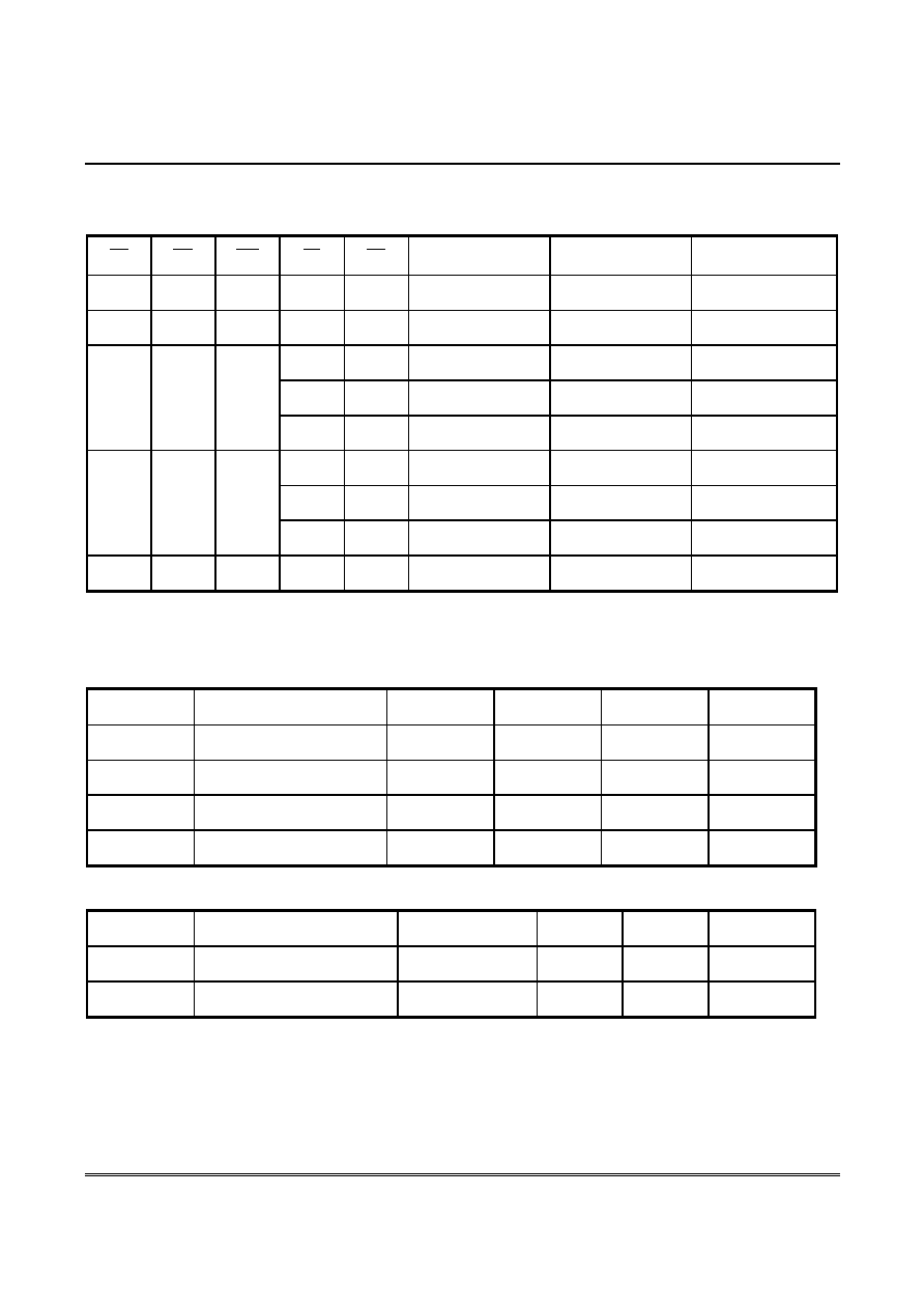
Truth Table
CE
OE
WE
LB
HB
I/O
1
to I/O
8
Mode
I/O
9
to I/O
16
Mode
VCC Current
H X X X X Not
selected
Not
selected I
SB1
, I
SB
X
X
X
H
H
High � Z
High � Z
I
SB1
, I
SB
L L
Read
Read
I
CC1
, I
CC2
, I
CC
L L H L H Read
High
�
Z
I
CC1
, I
CC2
, I
CC
H
L
High � Z
Read
I
CC1
, I
CC2
, I
CC
L L
Write
Write
I
CC1
, I
CC2
, I
CC
L X L L H Write
High
�
Z
I
CC1
, I
CC2
, I
CC
H
L
High � Z
Write
I
CC1
, I
CC2
, I
CC
L
H
H
X
X
High � Z
High � Z
I
CC1
, I
CC2
, I
CC
Note: X = H or L
Recommended DC Operating Conditions (
T
A
= -40
�
C to + 85
�
C )
Symbol Parameter Min.
Typ.
Max.
Unit
VCC Supply
Voltage
2.7
3
3.6
V
GND
Ground
0 0 0 V
V
IH
Input High Voltage
2.2
-
VCC + 0.3
V
V
IL
Input Low Voltage
-0.3
-
+0.6
V
Capacitance
( T
A
= 25
�
C, f = 1.0MHz )
Symbol Parameter Conditions
Min.
Max.
Unit
C
IN
* Input
Capacitance
V
IN
= 0V
6
pF
C
I/O
*
Input / Output Capacitance
V
I/O
= 0V
8
pF
* These parameters are sampled and not 100% tested.

ESMT
M23L416256A
Elite Semiconductor Memory Technology Inc.
Publication Date : Mar. 2003
Revision : 1.0
4/12
Absolute Maximum Ratings*
VCC to GND .............................................. -0.5V to +4.6V
IN, IN/OUT Volt to GND................... -0.5V to VCC + 0.5V
Operating Temperature, Topr ...................-40
�
C to +85
�
C
Storage Temperature, Tstg.....................-55
�
C to +125
�
C
Power Dissipation, P
T.......................................................................
0.7W
Soldering Temp. & Time ............................ 260
�
C, 10 sec
*Comments
Stresses above those listed under "Absolute Maximum Ratings" may cause permanent damage to this device. These are
stress ratings only. Functional operation of this device at these or any other conditions above those indicated in the
operational sections of this specification is not implied or intended. Exposure to the absolute maximum rating conditions for
extended periods may affect device reliability.
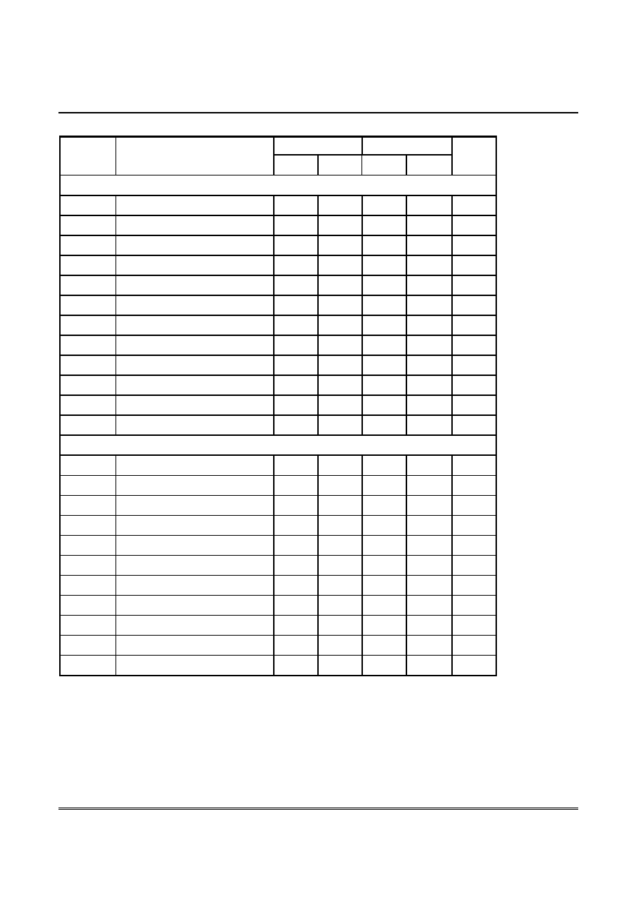
DC Electrical Characteristics
( T
A
= -40
�
C to + 85
�
C, VCC = 2.7 V to 3.6V )
M23L416256A-55/70
Unit
Symbol Parameter
Conditions
Min. Typ. Max.
I
LI
Input Leakage Current
V
IN
= GND to VCC
- - 1
�
A
I
LO
Output Leakage Current
CE = V
IH
OE = V
IH
or
WE = V
IH
V
I/O
= GND to VCC
-
-
1
�
A
I
CC1
Min. Cycle, Duty = 100%,
V
IN =
V
IL
or
V
IN =
V
IH
CE = V
IL
, I
I/O
= 0mA, V
DD =
3.3V
- - 45
mA
I
CC2
Operating Current
CE = V
IL
, I
I/O
= 0 mA
V
IN
Vcc-0.2 or V
IN
0.2V,
f = 1MHz, Duty = 100%,
- - 5
mA
I
SB
TTL Standby Current
CE = V
IH
- - 1.0
mA
L
*1
- - 40
�
A
I
SB1
CMOS Standby Current
CE
VCC - 0.2V, V
IN
0V
S
*1
10
�
A
V
OL
Output Low Voltage
I
OL
= 2 mA
-
-
0.4
V
V
OH
Output High Voltage
I
OH
= -1.0 mA
2.4
-
V
Notes *1 : L means Low power , S means Super Low Power.
ESMT
Preliminary M23L416256A
Elite Semiconductor Memory Technology Inc.
Publication Date : Mar. 2003
Revision : 1.0
5/12
AC Characteristics
( T
A
= -40
�
C to +85
�
C, VCC = 2.7V to 3.6V )
M23L416256A-55 M23L416256A-70
Symbol Parameter
Min. Max. Min. Max.
Unit
READ CYCLE
T
RC
Read
Cycle
Time
55
-
70
-
ns
T
AA
Address Access Time
-
55
-
70
ns
T
ACE
Chip Enable Access Time
-
55
-
70
ns
T
BE
Byte Enable Access Time
-
55
-
70
ns
T
OE
Output Enable to Output Valid
-
25
-
35
ns
T
CLZ
Chip Enable to Output in Low Z
10
-
10
-
ns
T
BLZ
Byte Enable to Output in Low Z
10
-
10
-
ns
T
OLZ
Output Enable to Output in Low Z
5
-
5
-
ns
T
CHZ
Chip Disable to Output in High Z
-
20
-
25
ns
T
BHZ
Byte Disable to Output in High Z
-
20
-
25
ns
T
OHZ
Output Disable to Output in High Z
-
20
-
25
ns
T
OH
Output Hold from Address Change
10
-
10
-
ns
WRITE CYCLE
T
WC
Write Cycle Time
55
-
70
-
ns
T
CW
Chip Enable to End of Write
45
-
60
-
ns
T
BW
Byte Enable to End of Write
45
-
60
-
ns
T
AS
Address Setup Time
0
-
0
-
ns
T
AW
Address Valid to End of Write
50
-
60
-
ns
T
WP
Write Pulse Width
40
-
50
-
ns
T
WR
Write Recovery Time
0
-
0
-
ns
T
WHZ
Write to Output in High Z
-
20
-
20
ns
T
DW
Data to Write Time Overlap
25
-
30
-
ns
T
DH
Data Hold from Write Time
0
-
0
-
ns
T
OW
Output Active from End of Write
5
-
5
-
ns
Note: t
CHZ
, t
BHZ
and t
OHZ
and t
WHZ
are defined as the time at which the outputs achieve the open circuit
Condition and are not referred to output voltage levels.