 | –≠–ª–µ–∫—Ç—Ä–æ–Ω–Ω—ã–π –∫–æ–º–ø–æ–Ω–µ–Ω—Ç: ES2838 | –°–∫–∞—á–∞—Ç—å:  PDF PDF  ZIP ZIP |
ESS Technology, Inc.
SAM0316-062702 1
ESS Technology, Inc.
ES2838
V.90/V.92 PCI HSP Modem
Product Brief
DESCRIPTION
The ES2838 is a high-performance, single-chip, Host-based
Signal Processing (HSP) modem solution that delivers high
connectivity and throughput without the need for a dedicated
Digital Signal Processing (DSP) unit. With the addition of an
external transformer DAA, the ES2838 TeleDrive
modem chip
provides a very low-cost modem solution for add-in cards,
desktops, and notebooks.
The ES2838 modem is capable of send/receive data and fax. It
supports Telephone Answering Machine (TAM) functions and
can handle data/fax/voice call discrimination. With its built-in
ACPI and D3
cold
wake-on-ring support, the ES2838 is an ideal
modem solution for notebooks and battery-operated devices.
The ES2838 includes a PCI bus interface and a codec. It also
includes ADC and DAC conversion of modem/voice signal data
and provides the interface and control logic needed to transfer
data between its serial I/O terminals and the PCI interface. The
ES2838 ADC and DAC operate synchronously, so that data
reception at the ADC channel and data transmission from the
DAC channel occur during the same time interval.
All of the Microsoft Windows Hardware Qualification Labs
(WHQL) certification requirements, as well as V.250, V.251, and
V.253 commands are met by the ES2838 modem solution.
The ES2838 is available in a 100-pin Low-profile Quad Flat Pack
(LQFP) package.
FEATURES
∑
V.90/V.92 analog data/fax/TAM modem.
∑
Caller ID.
∑
Data/fax/voice call discrimination.
∑
Data mode capabilities:
--≠
V.90/V.92: 56 kbps
--≠
ITU-T V.34: 33.6 kbps and fallbacks
--≠
V.42 and MNP error correction
--≠
V.42bis/MNP5 and V.44 data compression.
∑
Fax mode capabilities:
--≠
ITU-T V.17, V.29, V.27ter, and V.21ch2
--≠
Group 3 (TIA/EIA-578 Class 1 and Class 2).
∑
Requires minimum 166-MHz Pentium with MMX technology.
∑
PC2001-compliant.
∑
V.80 (H.324 software-stack -compatible).
∑
Worldwide homologation.
∑
D3
cold
Wake-on-Ring with ACPI 2.0.
∑
16-bit ADC and DAC with built-in anti-aliasing and
reconstruction filters.
∑
Separate analog (5V) and digital (3.3V with 5V-tolerant input
pads) power supplies.
∑
Internal PLL requiring a lower-frequency crystal for 18.816-MHz
input.
∑
EEPROM interface for subsystem vendor ID.
∑
Microsoft Windows
Unimodem V and TAPI specifications.
∑
Microsoft Windows
98/SE/ME/2000/XP.
∑
Microsoft Windows NT 4.0.
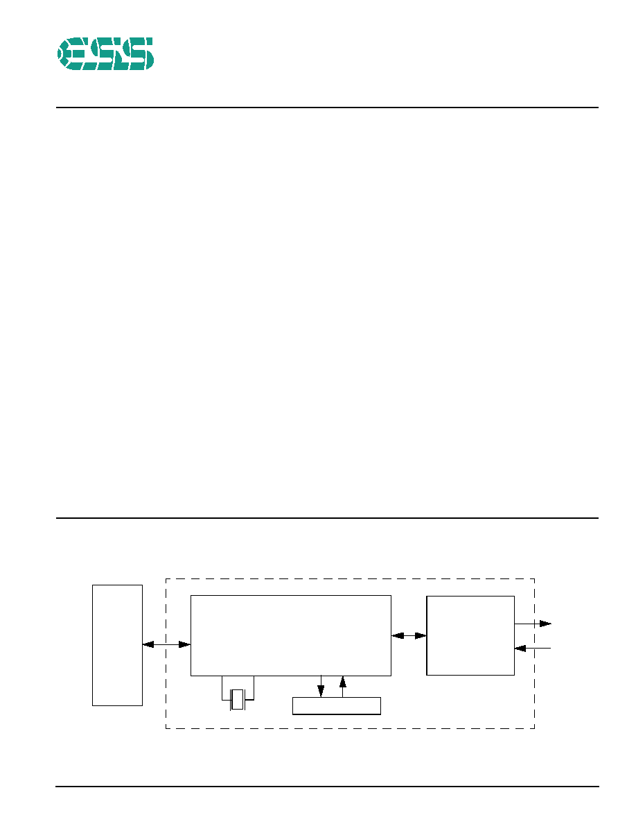
SYSTEM BLOCK DIAGRAM
Figure 1 shows the ES2838 system block diagram.
Figure 1 ES2838 System Block Diagram
ES2838
PCI BUS
DAA
PHONE
LINE
SERIAL EEPROM
MINI-PCI
OR
HSP MODEM
TRANSFORMER
2
SAM0316-062702
ESS Technology, Inc.
ES2838 PRODUCT BRIEF
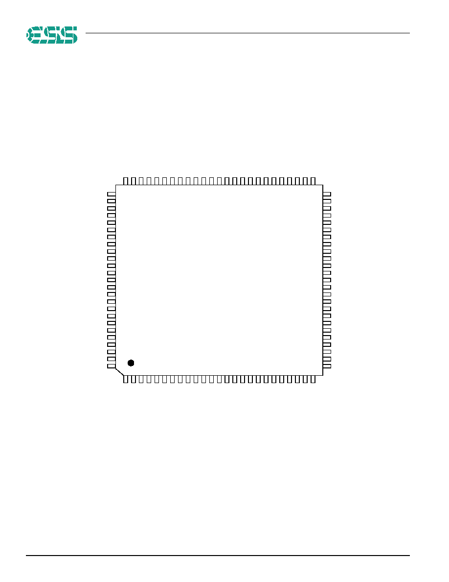
ES2838 PINOUT
Figure 2 shows the ES2838 pinout diagram.
Figure 2 ES2838 Pinout Diagram
27
1
50
49
48
47
46
45
44
43
42
41
40
39
38
37
36
35
34
33
32
31
2
3
4
5
6
7
8
9
10
11
12
13
14
15
16
17
18
19
20
21
22
23
24
25
30
29
28
26
75
74
73
72
71
70
69
68
67
66
65
64
63
62
61
60
59
58
57
56
55
54
53
52
51
76
77
78
79
80
81
82
83
84
85
86
87
88
89
90
91
92
93
94
95
96
97
98
99
100
ES2838S
100-Pin LQFP
V D D
CBE3#
GND
ID
S
E
L
AD1
6
AD1
7
AD1
8
AD1
9
AD2
0
AD2
1
AD2
2
AD2
3
VDD
FRAM
E#
GND
IRDY#
ST
OP#
CBE2#
TRDY#
DEV
SEL#
AD1
4
AD1
5
GND
C
BE1#
PA
R
A D 9
A D 1 0
A D 11
A D 1 2
A D 8
C B E 0 #
G N D
A D 0
A D 1
A D 2
A D 3
A D 4
A D 5
A D 6
A D 7
V D D
AD13
S E C S
S E D I
S E C L K
S E D O
VDD
V D D
P F 2
P F 4
P F 5
CURLIM#
D
PBX#
COMPLX#
D
SPK/PF1
1
CL
K
R
UN
#
GND
A D 3 1
A D 3 0
A D 2 9
A D 2 8
A D 2 7
A D 2 6
A D 2 5
A D 2 4
VA U X P
G N D
P C I C L K
I N TA #
R S T #
VA U X
P M E #
V D D
PF1
AGND
VDD
OSCI
OSCO
N C
NC
NC NC
OFFHOOK/
PF6
GN
D
AV
D
D
NC
NC
A G N D
A G N D
VRE
F
VCM
RXP
R I N G _ I N / P F 0
T X P
T X N
A G N D
RXN
A V D D
GND
L C S / P F 3
ESS Technology, Inc.
SAM0316-062702
3
ES2838 PRODUCT BRIEF
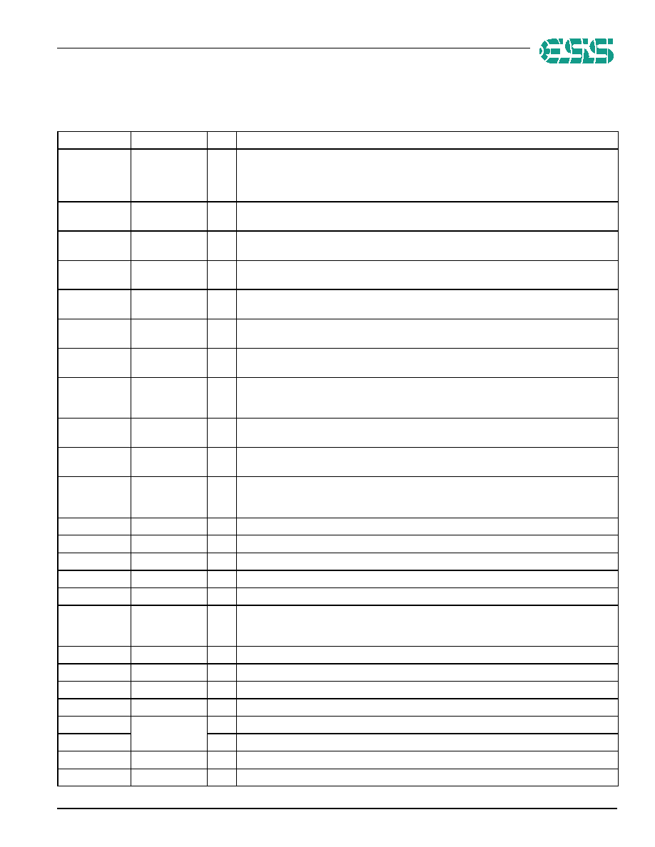
ES2838 PIN DESCRIPTIONS
Table 1 lists the ES2838 pin descriptions.
Table 1 ES2838 Pin Descriptions
Names
Pin Numbers
I/O
Definitions
C/BE3:0#
1, 13, 21, 31
I/O
Multiplexed bus command/byte enable. These pins indicate cycle type during the
address phase of a transaction. They indicate active-low byte enable information for the
current data phase during the data phases of a transaction. These pins are inputs during
slave operation and outputs during bus mastering operation.
IDSEL
2
I
Initialization device select, active-high. Used as a chip select during PCI configuration
read and write cycles.
GND
3, 15, 22, 41,
52, 61, 91
G
Digital ground.
VDD
12, 32, 46, 51,
58, 89, 100
P
Digital voltage [VDD (3.3V)].
AD31:0
4:11, 23:30,
33:40, 92:99
I/O
Address and data.
FRAME#
14
I/O
Cycle frame, active-low. The current PCI bus master drives this pin to indicate the
beginning and duration of a transaction.
IRDY#
16
I/O
Initiator ready, active-low. The current PCI bus master drives this pin to indicate that as
the initiator it is ready to transmit or receive data (and complete the current data phase).
TRDY#
17
I/O
Target ready, active-low. The current PCI bus master drives this pin to indicate that as
the target device it is ready to transmit or receive data (and complete the current data
phase).
DEVSEL#
18
I/O
Device select, active-low. The PCI bus target device drives this pin to indicate that it has
decoded the address of the current transaction as its own chip select range.
STOP#
19
I/O
Stop transaction, active-low. The current PCI bus target drives this pin active to indicate
a request to the master to stop the current transaction.
PAR
20
I/O
Parity, active-high. Indicates even parity across AD[31:0] and C/BE[3:0]# for both
address and data phases. The signal is delayed one PCI clock from either the address
or data phase for which parity is generated.
SEDO
42
I
Serial EPROM data output with internal pullup.
SEDI
43
O
Serial EPROM data input.
SECLK
44
O
Serial EPROM data clock input with internal pulldown.
SECS
45
O
Serial EPROM port chip select with internal pulldown.
LCS / PF3
48
I
General-purpose programmable flag: typically used as local current sense input.
PF[5:4] and
PF[2:1]
47, 49, 50, 64
I/O
General-purpose programmable bidirectional flag. Can be used for interfacing with a
telephone or other device, performing phone off-hook, phone on-hook, ring, and caller
ID functions.
CURLIM#
53
O
Current limit control output.
COMPLX#
54
O
Complex impedance select output.
DPBX#
55
I
Digital PBX detection input.
CLKRUN#
56
I/O
PCI clock state for power management.
DSPK
57
O
Modem speaker digital output.
PF11
O
General-purpose programable flag.
OSCI
59
I
18.816-MHz crystal oscillator input.
OSCO
60
O
18.816-MHz crystal oscillator output.
4
http://www.esstech.com
© 2002 ESS Technology, Inc. All rights reserved.
SAM0316-062702
ES2838 PRODUCT BRIEF
No part of this publication may be reproduced, stored in a
retrieval system, transmitted, or translated in any form or
by any means, electronic, mechanical, manual, optical, or
otherwise, without the prior written permission of ESS
Technology, Inc.
ESS Technology, Inc. makes no representations or
warranties regarding the content of this document.
All specifications are subject to change without prior
notice.
ESS Technology, Inc. assumes no responsibility for any
errors contained herein.
TeleDrive is a registered trademark of ESS Technology, Inc.
U.S. patents pending.
All other trademarks are owned by their respective
holders and are used for identification purposes only.
ESS Technology, Inc.
48401 Fremont Blvd.
Fremont, CA 94538
Tel: (510) 492-1088
Fax: (510) 492-1898
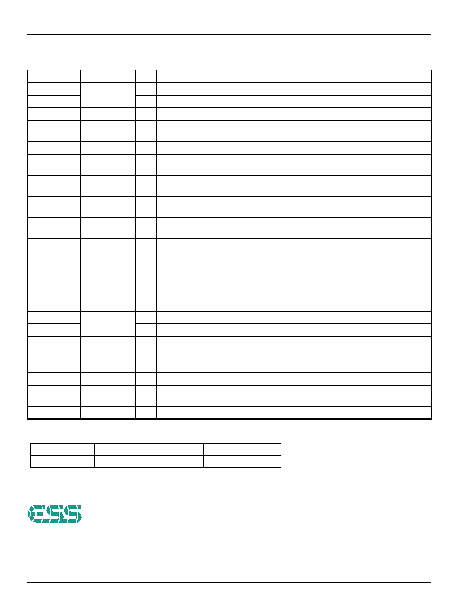
ORDERING INFORMATION
OFFHOOK
63
O
Offhook output driving 5V.
PF6
O
General-purpose programmable flag.
AVDD
65, 82
P
Analog voltage pins [AVDD (5V)].
NC
66, 67, 69, 70,
75, 76
--
No connect.
AGND
68, 77, 78, 81
G
Analog ground.
RXN
71
I
Codec analog differential negative input. The DC level is CVM, and the full-scale input is
either 0.22 Vp-p ±5% or 1.1 Vp-p±5%, depending on the gain setting.
RXP
72
I
Codec analog differential positive input. The DC level is CVM, and the full-scale input is
either 0.22 Vp-p ±5% or 1.1 Vp-p±5%, depending on the gain setting.
VREF
73
O
Voltage reference bypass. Has a range of 1.2356V±5%. Bypass to AGND with 0.1-
µF
ceramic chip capacitor parallel with 10-
µF tantalum capacitor.
VCM
74
O
Common mode voltage bypass. Has a range of 2.16V±5%. Bypass to AGND with 0.1-
µF
ceramic chip capacitor parallel with 10-
µF tantalum capacitor.
TXN
79
O
Codec negative analog output. The DC level is CVM, and the full-scale AC output is
2.8V p-p±5%. The maximum loading is 1 k
in parallel with 20 pF for modem
applications.
TXP
80
O
Codec positive analog output. The DC level is CVM, and the full-scale AC output is 2.8V
p-p±5%. The maximum loading is 1 k
in parallel with 20 pF for modem applications.
VAUX
83
P
Power to device during implementation of the D3
cold
state required by PCI Power
Management Interface specification.
RING_IN
84
I
RING_IN function, using a Schmitt trigger.
PF0
O
General-purpose programable flag.
PME#
85
O
Power management enable interrupt output to wake up the system.
VAUXP
86
I
V
AUX
support detection. V
AUXP
pin is driven high to indicate that ACPI is supported with
D3
cold
state. No V
AUX
support when driven low.
RST#
87
I
Active-low reset input.
INTA#
88
O
Interrupt request, active-low. The level triggered interrupt pin dedicated to servicing
internal device interrupt sources.
PCICLK
90
I
System bus clock input.
Table 1 ES2838 Pin Descriptions (Continued)
Names
Pin Numbers
I/O
Definitions
Part Number
Description
Package
ES2838S
V.90/V.92 PCI HSP Modem
100-pin LQFP