
ESS Technology, Inc.
SAM0376-091301
1
ESS Technology, Inc.
ES2845S/ES2851S
HomePNA/LAN/V.90/V.92 HSP Solution
Product Brief
DESCRIPTION
The ES2845S/ES2851S SuperLink
TM-
MLP16 solution provides
the first true simultaneous, concurrent, triple-technology
connectivity: 16 Mbps Home Phoneline Networking Alliance
(HomePNA 2.0), 10/100 IEEE 802.3 Fast Ethernet LAN, and
V.90/V.92 56k HSP modem. This triple-technology solution
enables end users to enjoy the increased flexibility needed in
today's complex world of communications.
The ES2845S combines a HomePNA 2.0-compliant MAC/PHY
device, a 10/100 IEEE 802.3 MAC device, and a V.90/V.92 56k
HSP modem with an analog telephone line interface and a PCI
2.2-compliant bus interface designed into the device
architecture. This advanced high-level dual-MAC device
integration allows the use of the ES2845S for desktop and laptop
systems as a host-based modem solution, a 10/100 Ethernet
connection, or a home network connection that complies with the
16-Mbps (HomePNA 2.0) specification, either individually or
concurrently.
The ES2851S is the analog front end device for the SuperLink
-
MLP16 solution, and provides the HomePNA 2.0 line interface
functionality. Only minimal additional components, such as
resistive hybrids and assorted magnetics, are required to
implement the HomePNA 2.0 line interface functionality.
The ES2845S is available in an industry-standard 128-pin low-
profile quad flat pack (LQFP) package. The ES2851S is available
in an industry-standard 48-pin LQFP package.
HomePNA FEATURES
�
Fully compliant with HPNA 2.0 collision resolution
specification for packet buffering, collision detection, and
retransmission logic.
�
Adaptive equalizer for robust packet filtering over time
and impaired channels.
�
Address filtering.
�
Highly integrated MAC/PHY, supporting both HomePNA
2.0 and HomePNA 1.1:
-- ES2845S HomePNA/LAN/Modem.
-- ES2851S HomePNA AFE.
�
Compliant with HomePNA 10M8 (HomePNA 2.0) and
1M8 (HomePNA 1.1) Interface specifications:
-- Automatic mode configuration switches between
Home PNA 2.0/1.1 modulation and protocol, based
on capabilities of the remote station on the network.
-- Supports automatic rate adaptation (HomePNA 2.0
4 Mbps to 16 Mbps).
�
Quality-of-service (QoS) support:
-- Eight-level packet priority.
-- Dynamic priority remapping.
-- Distributed fair priority queuing (DFPQ) MAC
extension for low-latency multimedia packets.
�
Compatible with existing telephone services:
-- Basic telephony (POTS).
-- G.992.1 DMT full-rate ADSL and G.992.2 G.Lite ADSL
-- ISDN voice and data services.
�
Integrated crystal oscillator.
�
10-bit current steering DAC.
�
12-bit ADC.
�
Variable gain amplifiers.
�
Line drivers.
LAN FEATURES
�
Highly integrated MAC supporting dual-speed
10/100-Mbps Ethernet LAN.
�
Wake-on-LAN and RJ-45 Ethernet connections.
�
Integrated media independent interface (MII) and
reduced media independent interface (RMII) for
connecting to external 10/100-Mbps PHY
transceiver.
�
Full-duplex operation support in both MII/RMII ports with
independent TX and RX channels.
MODEM FEATURES
�
V.90/V.92-D/F/TAM modem.
�
Integrated low-voltage DAA circuit.
�
Compliant with PC2001 system design guidelines.
�
Wake-on-ring, caller ID, and RJ-11 tip-and-ring
connections.
�
Worldwide homologation and ITU V.250, V.251, and
V.253.
POWER MANAGEMENT
�
Supports ACPI 2.0 and Rev 1.1 of PCI Bus Power
Management Interface Specification.
�
PCI 2.2 bus interface supports both 3.3V and 5.0V
signaling.
�
Separate 1.5V and 3.3V digital power supplies utilized.
�
Link integrity functions.
2
SAM0376-091301
ESS Technology, Inc.
ES2845S/ES2851S PRODUCT BRIEF
DRIVER SOFTWARE SUPPORT (HomePNA 2.0/
LAN)
�
Windows 98SE/ME/2000/XP.
�
NDIS 5.0.
DRIVER SOFTWARE SUPPORT (Modem)
�
Windows 98SE/ME/2000/XP.
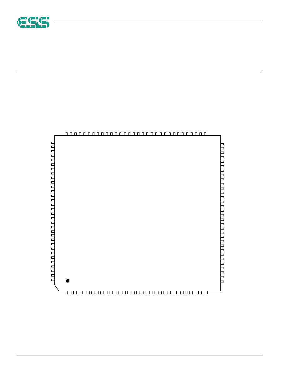
ES2845S PINOUT
Figure 1 depicts the device pinout for the ES2845S.
Figure 1 ES2845S Device Pinout
1
96
97
64
33
32
128
65
ES2845S
128-Pin LQFP
A
D
2
4
C
/
B
E
3
#
I
D
S
E
L
V
D
D
_
C
O
R
E
A
D
2
3
A
D
2
2
A
D
2
1
A
D
2
0
A
D
1
9
A
D
1
8
A
D
1
7
A
D
1
6
G
N
D
C
/
B
E
2
#
F
R
A
M
E
#
I
R
D
Y
#
T
R
D
Y
#
D
E
V
S
E
L
#
S
T
O
P
#
P
A
R
C
/
B
E
1
#
V
D
D
_
I
O
A
D
1
3
A
D
1
4
A
D
1
5
A
D
1
2
A
D
1
1
G
N
D
SERR#
AD10
AD9
AD8
C/BE0#
VDD_IO
AD7
AD6
AD5
AD4
AD3
AD2
AD1
AD0
VAUX_IO
PWR_RST#
RST_PHY#
ECS
RXER/RX_ER
RXDV/CRS_DV
COL/SPEED10
CRS
RXCLK
GND
RXD0
RXD1
RXD2
RXD3
GND
IRQ#
EDIN
VAUX_CORE
E
C
L
K
E
D
O
U
T
V
A
U
X
_
I
O
M
D
I
O
M
D
C
/
R
M
I
I
_
M
O
D
E
T
X
C
L
K
/
R
E
F
C
L
K
G
N
D
G
N
D
T
X
D
2
T
X
D
1
T
X
D
0
T
X
D
3
L
I
N
K
_
S
T
1
S
L
_
P
W
D
N
V
A
U
X
_
C
O
R
E
V
A
U
X
_
C
O
R
E
S
L
_
R
X
5
S
L
_
R
X
4
S
L
_
R
X
3
S
L
_
R
X
0
S
L
_
R
X
1
S
L
_
R
X
2
S
L
_
C
L
K
V
A
U
X
_
P
L
L
G
N
D
_
P
L
L
S
L
_
T
X
4
S
L
_
T
X
0
S
L
_
T
X
1
S
L
_
T
X
2
S
L
_
T
X
3
S
L
_
R
S
T
#
T
X
E
N
AD29
AD30
AD31
PCIREQ#
PCIGNT#
GND
VDD_IO
CLKRUN#
INTA#
GND
PCICLK
PCIRST#
GND
WOL/VAUXP
OSCI
VAUX_IO
OSCO
NC
VDD_IO
DSPK
GND
PME#
ISO_GND
LINK_LED#
ACT_LED#
VAUX_CORE
SL_MODE0
SL_MODE1
ISO_SIG
116
GND
ISOB
117
118
119
120
121
122
123
124
125
126
127
115
114
113
112
111
110
109
108
107
106
105
104
103
102
101
100
99
98
95 94 93
66
67
68
69
70
71
72
73
74
75
76
77
78
79
80
81
82
83
84
85
86
87
88
89
92 91 90
63
62
61
60
59
58
57
56
55
54
53
52
51
50
49
48
45
44
34
35
36
37
38
39
43
42
41
40
31
30
29
28
27
26
25
24
23
22
21
20
19
18
17
16
2 3 4 5 6 7 8 9 10 11 12 13 14 15
46
47
NC
A
D
2
5
A
D
2
6
A
D
2
7
A
D
2
8

ESS Technology, Inc.
SAM0376-091301
3
ES2845S/ES2851S PRODUCT BRIEF
ES2845S PIN DESCRIPTION
Table 1 lists the pin descriptions for the ES2845S.
Table 1 ES2845S Pin Description
Names
Pin Numbers
I/O
Definitions
AD[31:0]
126:128, 1:5, 9:16,
27:31, 34:36, 39:46
I/O
Address and data lines from the PCI bus.
C/BE[3:0]#
6, 18, 25, 37
I/O
PCI command/byte enable. During address phase of a transaction, these pins
define the bus command. During data phase, these pins define the byte enable.
IDSEL
7
I
ID select.
VDD_CORE
8
P
1.5V VDD core power supply.
GND
17, 32, 56, 57,
71, 72, 99,
109, 110, 122, 123
G
Ground.
FRAME#
19
I/O
Cycle frame.
IRDY#
20
I/O
Initiator ready.
TRDY#
21
I/O
Target ready.
DEVSEL#
22
I/O
Device select .
STOP#
23
I/O
Stop transaction.
PAR
24
I/O
Parity.
VDD_IO
26, 38, 116, 117
P
3.3V VDD I/O power supply.
SERR#
33
O
System bus error.
VAUX_IO
47, 67, 113
P
3.3V V
AUX
I/O power supply.
PWR_RST#
48
I
Power-on reset. This is an active-low input signal when a power-on-reset event
occurs.
ECS
49
O
EEPROM chip select output for Ethernet/HomePNA.
RST_PHY#
50
O
Reset Ethernet PHY.
RXER
51
I
Receive error input for MII mode. Indicates that external Ethernet PHY transceiver
has detected coding errors in receive data frame currently being transmitted to
RXD[3:0]. RXER is ignored while RXDV is deasserted.
RX_ER
I
Receive error input for RMII mode. Indicates that external Ethernet PHY transceiver
has detected coding errors in receive data frame currently being transmitted to
RXD[1:0]. RX_ER is ignored while RX_DV is deasserted.
RXDV
52
I
Receive data valid from external Ethernet PHY. When selected as RXDV input, indi-
cates valid received data is being presented to RXD[3:0] and that RXCLK is syn-
chronous to the receive data. Asserted before rising edge of RXCLK and remains
asserted until after rising edge of RXCLK.
CRS_DV
I
Carrier sense/receive data valid. Asserted asynchronously by the external Ethernet
PHY when the receive medium is nonidle. In 10Base-T mode, carrier is detected
when squelch is passed in RMII mode.
COL
53
I
Collision. When selected as COL, asserted by external Ethernet PHY whenever a
collision is detected.
SPEED10
I
Speed select. Acts as toggle for 10-Mbps and 100-Mbps operation for external
Ethernet PHY transceiver in RMII mode.
CRS
54
I
Carrier sense input from external Ethernet PHY.

4
SAM0376-091301
ESS Technology, Inc.
ES2845S/ES2851S PRODUCT BRIEF
RXCLK
55
I
Receive clock input. Provides the nibble rate clock timing reference for the
output transfer of RXDV, RXD[3:0], and RXER signals in MII mode.
Provides the
nibble rate clock timing reference for the output transfer of CRS_DV,
RXD[1:0] and RX_ER in RMII mode.
Operates at 2.5 MHz in 10 Mb/s
(10Base-T) mode and 25 MHz in 100 Mb/s (100Base-T) mode.
IRQ#
58
I
Interrupt request from external Ethernet PHY (active-low).
RXD[3:0]
62:59
I
Receive data input pins from external Ethernet PHY. In RMII mode, only RXD[1:0]
are defined.
VAUX_CORE
63, 80, 81, 106
P
1.5V V
AUX
core power supply.
EDIN
64
I
EEPROM data input for both Ethernet and HomePNA functions.
ECLK
65
O
EEPROM clock output for both Ethernet and HomePNA functions.
EDOUT
66
O
EEPROM data output for Ethernet and HomePNA functions.
MDIO
68
I/O
Functions as the MII management data input/output from external Ethernet PHY.
Acts as an output during the header portion of management frame transfers and
during the data portion of write operations. Also acts as an input during the data por-
tion of read operations.
MDC
69
O
MII Management Data Clock output to external Ethernet PHY.
RMII_MODE
I
RMII_MODE enable. Strap option pin latched at power-on reset. The ES2845S sup-
ports both the MII and RMII modes of operation. When the RMII_MODE
signal is high, the RMII mode of operation is supported. When the RMII_MODE sig-
nal is low at power-on reset, at power-on reset, the MII mode of operation is sup-
ported.
TXCLK
70
I
Transmit clock input from external Ethernet PHY. When selected as TXCLK, pro-
vides timing reference for transfer of the transmitted data in MII mode.
Operates at 2.5 MHz in 10 Mb/s (10Base-T) mode and at 25 MHz in 100 Mb/s
(100Base-T) mode.
REFCLK
I
Reference clock input. When selected as REFCLK, provides continuous clock tim-
ing reference from MAC engine for CRS_DV, RXD[1:0], TXEN, TXD[1:0], and
RX_ER in RMII mode. Operates at 50 MHz �50 ppm, with a duty cycle between
35% and 65% in RMII mode.
TXEN
73
O
Transmit enable pin to external Ethernet PHY. This pin indicates that ES2845S is
presenting valid data on TXD[3:0].
TXD[3:0]
77:74
O
Transmit data output pins to external Ethernet PHY. In RMII mode, only TXD[1:0]
are defined.
LINK_ST1
78
I
Link status Interface input from external Ethernet PHY.
SL_PWDN
79
O
Power down control output pin to ES2851S.
SL_RX[5:0]
87:82
I
Receive data input pins from ES2851S.
SL_CLK
88
I
Crystal clock input from ES2851S, operated at 64 MHz.
VAUX_PLL
89
P
1.5V V
AUX
PLL power supply.
GND_PLL
90
G
Ground for internal PLL.
SL_TX[4:0]
95:91
O
Transmit data output to ES2851S.
SL_RST#
96
O
Reset output to ES2851S (active-low).
SL_MODE
[1:0]
98:97
O
Mode select output pins to ES2851S.
Table 1 ES2845S Pin Description (Continued)
Names
Pin Numbers
I/O
Definitions

ESS Technology, Inc.
SAM0376-091301
5
ES2845S/ES2851S PRODUCT BRIEF
ISO_SIG
100
I/O
DAA module isolation signal interface input/output.
ISOB
101
O
Analog supply voltage.
ISO_GND
102
I
DAA module isolation ground.
PME#
103
O
Power management enable interrupt output to wake up the system.
LINK_LED#
104
O/D Open drain pin; indicator of good link for Home PNA PHY operation.
ACT_LED#
105
O/D Open drain pin; link activity indicator at transmit or receive data.
NC
107, 115
--
No connect.
VAUXP
108
I
Strap option pin. V
AUX
support detection pin. V
AUXP
is driven high at reset to indi-
cate that ACPI is supported with D3
cold
state. No support when driven low.
WOL
O
Wake-on-LAN signal output. The ES2845S asserts this signal if a change is
detected in link status, Magic Packet
TM,
or sample frame events.
OSCI
111
I
Crystal clock input operates at 19.6608 MHz to use on-chip silicon DAA module.
OSCO
112
O
Crystal clock output.
DSPK
114
O
Modem speaker digital output.
CLKRUN#
118
I/O
Input/output for PCI clock status and output to start or accelerate clock function.
INTA#
119
OD
Interrupt A request output, active-low. INTA# is the level triggered interrupt pin dedi-
cated to servicing internal device interrupt requests.
PCIRST#
120
I
PCI bus reset.
PCICLK
121
I
PCI bus clock input.
PCIGNT#
124
I
PCI grant input.
PCIREQ#
125
O
PCI request output.
Table 1 ES2845S Pin Description (Continued)
Names
Pin Numbers
I/O
Definitions