 | –≠–ª–µ–∫—Ç—Ä–æ–Ω–Ω—ã–π –∫–æ–º–ø–æ–Ω–µ–Ω—Ç: ES3207 | –°–∫–∞—á–∞—Ç—å:  PDF PDF  ZIP ZIP |
ESS Technology, Inc.
SAM0076-051701
1
ES3207
Video CD/DVD Companion Chip
Product Brief
DESCRIPTION
The ES3207 Video CD/DVD Companion Chip provides an
optimal system design for a Video CD player or a DVD
player.
The ES3207, which is an enhanced version of the pin-
compatible ES3205, integrates most of the required
analog discrete components into a simple, cost-effective
solution and interfaces directly to the ES3210 (Video CD)
or ES3308 (DVD). No glue logic or external microcontroller
is required.
The ES3207 features include a high-quality NTSC/PAL
Digital Video Encoder (DVE), echo, echo reverb,
3DSound, surround sound, video and audio DACs, and a
PLL clock synthesizer. There are three 9-bit video DACs
(one for composite video output and two for S-video
outputs) and two 16-bit sigma-delta audio DACs for
interfacing with current sound systems.
The DVE generates composite and S-video analog
signals. Color Space Conversions (CSC) are provided to
match the input data to the required output format, then
the data is filtered to meet the selected video standards. In
addition, the ES3207 is equipped with a remote control
interface for power on/off, microphone ports, auxiliary
ports, and an interface for accessing internal registers.
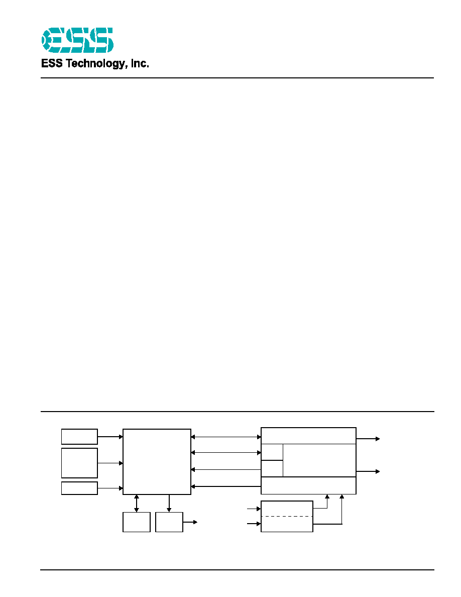
Figure 1 shows a block diagram of a typical stand-alone
system using the ES3210 Video CD Processor Chip or the
ES3308 MPEG2 Audio/Video Decoder Chip and an
ES3207 Video CD Companion Chip.
FEATURES
∑
Multi-standard TV encoder:
≠ CCIR601 non-square operation
≠ NTSC/PAL formats
≠ Master video mode
≠ 8-bit interface for YCrCb (4:2:2) input format
≠ Simultaneous composite and S-video output
≠ Interlaced operation
∑
Audio DACs:
≠ Two 16-bit sigma-delta DACs
≠ Accepts I
2
S format data
≠ Programmable functions
∑
3DSound and surround sound
∑
Remote control interface for power on/off
∑
Digitally controlled echo with up to 168 ms delay
∑
Vocal reverb for theater acoustical effects
∑
Dual microphone input
∑
Clock synthesizer (PLL):
≠ Based on 27 MHz crystal input
≠ Generates required clocks for video encoder, audio
DAC, echo and surround sound, and video
processor
∑
Device Serial Communication (DSC) port for command
issued/register access
∑
Power management
∑
100-Pin PQFP
∑
Single 5 V power supply
Figure 1 ES3207 Video CD Companion Chip System Block Diagram
ES3207
DRAM
Remote
VFD
VFD
Driver
Panel
Receiver
ES3210
CD-ROM
Audio DAC
3D/Echo/Surround
PLL
NTSC/PAL Video
DSC
ROM
Television
Speakers
(Video CD)
or
ES3308
(DVD)
or
DVD-ROM
Drive
Preamp
Volume Control
Preamp
Volume Control
Mic 1
Mic 2

2
SAM0076-051701
ESS Technology, Inc.
ES3207 VIDEO CD CC PRODUCT BRIEF
PINOUT
PINOUT
PIN DESCRIPTION
Name
Number
I/O
Definition
VSS
1:2,25:26,29:31,72,75,
77,91,100
I
Ground.
VCC
3:5,16,32,66,73,78,90
I
Voltage supply, 5 V.
DSC_C
6
I
Clock for programming to access internal registers.
AUX[15:0]
40:38,36:34,20,18,14,
67:70,11,9,7
I/O
Auxiliary control pins.
DSC_D[7:0]
81,83,85,93,95,97,99,8
I/O
Data for programming to access internal registers.
DSC_S
10
I
Strobe for programming to access internal registers.
DCLK
12
O
Dual-purpose pin. DCLK is the MPEG decoder clock.
EXT_CLK
I
EXT_CLK is the external clock. EXT_CLK is an input during bypass PLL mode.
RST#
13
I
Video reset (active-low).
MUTE
15
O
Audio mute.
MCLK
17
I
Audio master clock.
TWS
19
I
Dual-purpose pin. TWS is the transmit audio frame sync.
SPLL_OUT
O
SPLL_OUT is the select PLL output.
1
VSSA
MIC1
MIC2
AOL
AOR
VCCA
VCCA
VREFP
VREFM
VSSA
AUX15
AUX14
AUX13
RBCK / SER_IN
AUX12
AUX11
AUX10
RSD / SEL_PLL0
VCC
VSS
DSC_D7
HSYNC#
DSC_D6
VSYNC#
DSC_D5
YUV7
YUV6
YUV5
YUV4
VCC
VSS
YUV3
DSC_D4
YUV2
DSC_D3
YUV1
DSC_D2
YUV0
DSC_D1
VSS
TSD
AU
X
9
T
W
S /
SP
LL_O
UT
AU
X
8
MCLK
VC
C
MU
T
E
AU
X
7
RS
T#
DCLK
/ E
X
T_CLK
AU
X
2
DS
C_S
AU
X
1
DS
C_
D0
AU
X
0
DS
C
_
C
VC
C
VC
C
VS
S
VS
S
VS
S
VS
S
VC
C
NC
NC
VS
S
VS
S
RS
T
O
UT#
R
W
S
/
S
E
L_P
LL1
TB
CK
YD
A
C
VSS
A
VSS
A
VD
A
C
NC
VC
C
AU
X
6
AU
X
5
AU
X
4
AU
X
3
XO
U
T
VSS
VC
C
XI
N
VSS
NC
VSS
VC
C
PC
LK
PCLK
2X
VSS
A
VR
E
F
VC
M
RS
E
T
COMP
VSS
A
VSS
A
CDA
C
V
CCA
V
CCA
31
30
51
50
80
81
100
2
3
4
5
6
7
8
9
10 11 12 13 14 15 16 17 18 19 20 21 22 23 24 25 26 27 28 29
49
48
47
46
45
44
43
42
41
40
39
38
37
36
35
34
33
32
79 78 77 76 75 74 73 72 71 70 69 68 67 66 65 64 63 62 61 60 59 58 57 56 55 54 53 52
82
83
84
85
86
87
88
89
90
91
92
93
94
95
96
97
98
99
ES3207
ESS Technology, Inc.
SAM0076-051701
3
ES3207 VIDEO CD CC PRODUCT BRIEF
PIN DESCRIPTION
TSD
21
I
Transmit audio data input.
TBCK
22
I
Transmit audio bit clock.
RWS
23
O
Dual-purpose pin. RWS is the receive audio frame sync.
SEL_PLL1
I
Pins SEL_PLL[1:0] select the PLL clock frequency for the DCLK output.
RSTOUT#
24
O
Reset output (active-low).
NC
27:28,65:76
No connect. Do not connect to these pins.
RSD
33
O
Dual-purpose pin. RSD is the receive audio data input.
SEL_PLL0
I
SEL_PLL0 along with SEL_PLL1 select the PLL clock frequency for the DCLK out-
put. See the table for pin number 23.
RBCK
37
O
Dual-purpose pin. RBCK is the receive audio bit clock.
SER_IN
I
SER_IN is the serial input DSC mode.
0 = Parallel DSC mode.
1 = Serial DSC mode.
VSSA
41,50:51,56:57,62:63
I
Analog ground.
VREFM
42
I
DAC and ADC minimum reference. Bypass to VCMR with 10
µ
F in parallel with 0.1
µ
F.
VREFP
43
I
DAC and ADC maximum reference. Bypass to VCMR with 10
µ
F in parallel with 0.1
µ
F.
VCCA
44:45,59:60
I
Analog VCC, 5 V.
AOR
46
O
Right channel output.
AOL
47
O
Left channel output.
MIC2
48
I
Microphone input 2.
MIC1
49
I
Microphone input 1.
VREF
52
I
Internal resistor divider generates Common Mode Reference (CMR) voltage.
Bypass to analog ground with 0.1
µ
F.
VCM
53
I
ADC Common Mode Reference (CMR) buffer output. CMR is approximately 2.25 V.
Bypass to analog ground with 47
µ
F electrolytic in parallel with 0.1
µ
F.
RSET
54
I
Full scale DAC current adjustment.
COMP
55
I
Compensation pin.
CDAC
58
O
Modulated chrominance output.
YDAC
61
O
Y luminance data bus for screen video port.
VDAC
64
O
Composite video output.
XOUT
71
O
Crystal output.
XIN
74
I
27 MHz crystal input.
PCLK
79
I/O
13.5 MHz pixel clock.
PCLK2X
80
I/O
27 MHz (2 times pixel clock).
HSYNC#
82
O
Horizontal sync (active-low).
VSYNC#
84
O
Vertical sync (active-low).
YUV[7:0]
86:89,92,94,96,98
I
YUV data bus for screen video port.
Name
Number
I/O
Definition
SEL_PLL1
SEL_PLL0
DCLK
0
0
Bypass PLL (input mode)
0
1
27 MHz (output mode)
1
0
32.4 MHz (output mode)
1
1
40.5 MHz (output mode)
4
© 1997 ESS Technology, Inc. All rights reserved.
SAM0076-051701
ES3207 VIDEO CD CC PRODUCT BRIEF
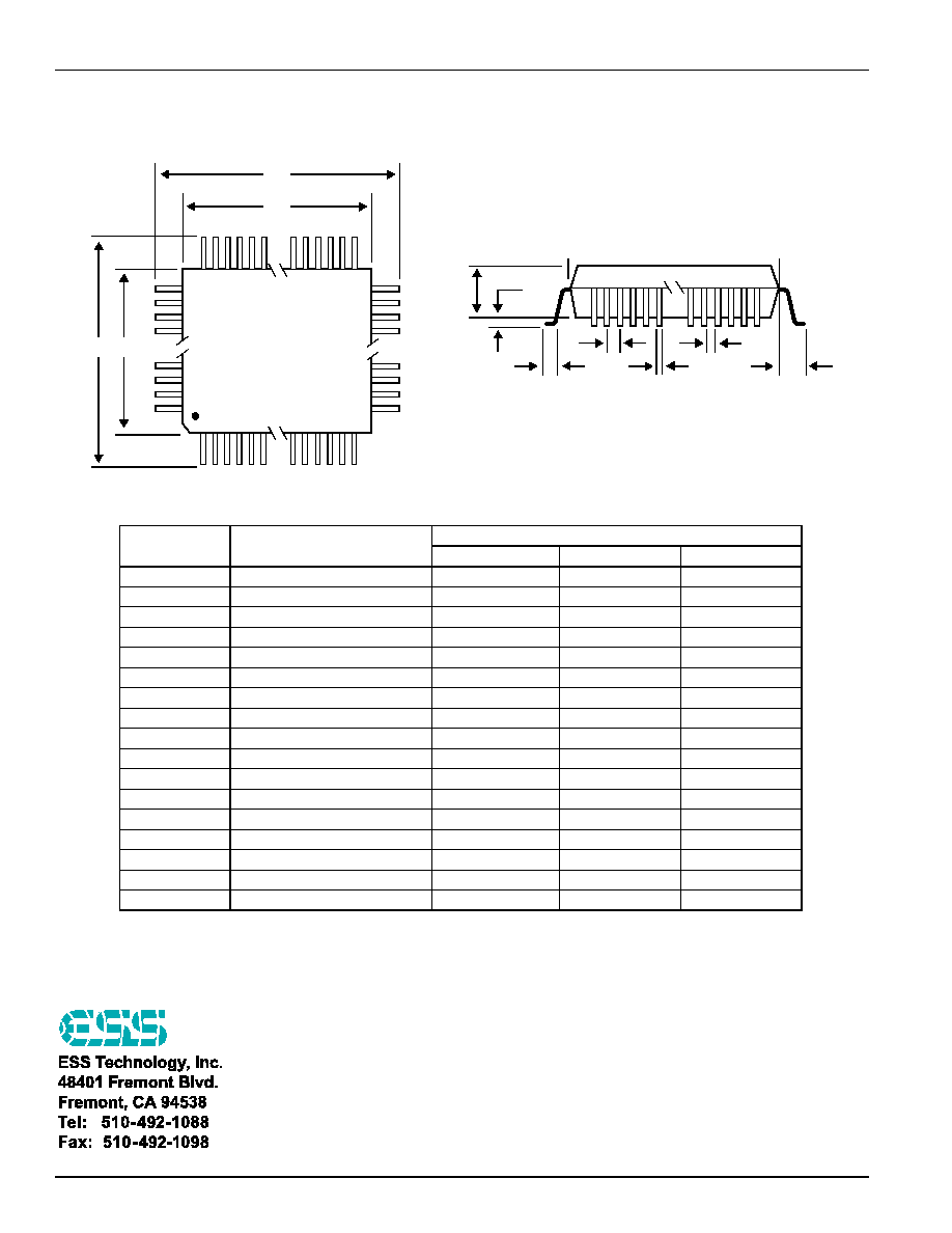
MECHANICAL DIMENSIONS
No part of this publication may be reproduced, stored in a
retrieval system, transmitted, or translated in any form or
by any means, electronic, mechanical, manual, optical, or
otherwise, without the prior written permission of ESS
Technology, Inc.
ESS Technology, Inc. makes no representations or
warranties regarding the content of this document.
All specifications are subject to change without prior
notice.
ESS Technology, Inc. assumes no responsibility for any
errors contained herein.
(P) U.S. Patent 4,214,125 and others, other patents
pending.
VideoDrive
Æ
is a registered trademark of ESS Technology,
Inc.
MPEG is the Moving Picture Experts Group of the ISO/IEC.
All other trademarks are owned by their respective
holders and are used for identification purposes only.
MECHANICAL DIMENSIONS
Symbol
Description
Millimeters
Min
Nom
Max
D
Lead to lead, X-axis
23.65
23.90
24.15
D1
Package's outside, X-axis
19.90
20.00
20.10
E
Lead to lead, Y-axis
17.65
17.90
18.15
E1
Package's outside, Y-axis
13.90
14.00
14.10
A1
Board standoff
0.10
0.25
0.36
A2
Package thickness
2.57
2.71
2.87
b
Lead width
0.20
0.30
0.40
e
Lead pitch
-
0.65
-
e1
Lead gap
0.24
-
-
L
Foot length
0.65
0.80
0.95
L1
Lead length
1.88
1.95
2.02
-
Foot angle
0∞
-
7∞
-
Coplanarity
-
-
0.102
-
Leads in X-axis
-
30
-
-
Leads in Y-axis
-
20
-
-
Total leads
-
100
-
-
Package type
-
PQFP
-
E1
A2
A1
L
E
D1
b
D
ES3207
e
1
e1
L1
100-Pin PQFP