ESS Technology, Inc.
SAM0241-052101
1
ES4408
DVD
Processor
Product Brief
DESCRIPTION
The ES4408 Processor is a single-chip solution for a Digital
Versatile Disc (DVD) player that integrates MPEG video
decoding, DVD system navigation, Content Scrambling System
(CSS), and DolbyTM Digital (AC-3) and MPEG audio decoding.
The fully programmable ES4408 is based on a proprietary ESS
architecture. It offers the best feature set in comparison to any
currently existing DVD chip, and a glueless interface to various
peripheral components. The ES4408 is the most cost effective
solution in its class with an integration level and quality that set
new benchmarks.
The ES4408 processor is capable of decoding DolbyTM Digital
(AC-3) up to 5.1 channels or MPEG audio up to 7.1 channels
simultaneously with MPEG-1 or MPEG-2 video. For embedded
applications, the ES4408's internal RISC processor can be used
in place of a microcontroller to provide all system control, DVD
system navigation, CSS decryption, and many other features.
On-chip, multi-tap filters provide arbitrary scaling with state of the
art SmartScaleTM technology useful for video standards
conversion. SmartStreamTM technology from ESS provides video
error concealment and video post-processing, leading to the
highest playability and video quality. Other features included in
the ES4408 are video letterbox display, DVD Sub-Picture
overlay, and On-Screen Display.
The ES4408 provides a glueless 8/16-bit parallel interface to
many DVD servo/loaders. It connects directly with 8/16-bit ROM
and 16-bit SDRAM/EDO. An 8-bit YUV video interface supports
many TV encoders. General purpose auxiliary pins are provided
to control various peripheral devices. A standard I
2
S interface
supports popular audio DACs and ADCs. The ES4408 also
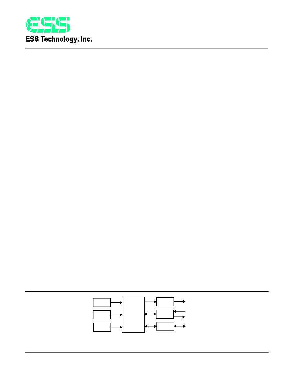
features a direct S/PDIF output. Figure 1 shows a block diagram
of a typical standalone system using the ES4408 with the
glueless SDRAM interface.
The DVD system stream from a DVD disc is passed to the TM
ES4408 through the 8-bit/16-bit parallel host interface. The TM
ES4408 parses the system layer and demultiplexes the audio
and video streams. Audio is decoded and passed through the I
2
S
audio serial bus to an external audio DAC and then to the
speakers. Video is decoded and output as YUV pixels to an
NTSC or PAL video encoder. System control and housekeeping
functions (keypad and remote control) are also provided on-chip.
FEATURES
�
Single-Chip DVD video decoder in a 208-pin PQFP package
�
Supports MPEG-1 system and MPEG-2 program streams
�
Programmable multimedia processor architecture
�
Compatible with Audio CD, VideoCD 1.1, 2.0, Interactive
VCD 3.0, and Super VideoCD (SVCD)
�
DVD Navigation 1.0
�
Built-in Content Scrambling System (CSS)
Video
�
Pan & Scan and Letter-Box conversions supported
�
Trick modes such as Slow, Fast Forward, Fast Reverse,
Step, and Goto supported
�
On-chip subpicture unit (SPU) decoder supports remote
control display functions
�
On-chip 4-bit On-Screen Display (OSD) controller with 4-bit
blending supports karaoke lyric and subtitile display
functions.
�
8-bit YUV output
Audio
�
Karaoke function
�
DolbyTM Digital (AC-3) up to 5.1 channels or 2-channel
downmix audio output for DolbyTM Pro Logic
�
MPEG audio up to 7.1 channel
�
Linear PCM streams for 48 KHz and up to 96 KHz
�
S/PDIF audio output
�
Supports 256/384/512 frame sync audio system clocks
Smart Technology
�
SmartZoomTM for motion zoom and pan
�
SmartScaleTM for NTSC to PAL conversion and vice versa
�
SmartStreamTM for video error concealment
Peripheral
�
Bidirectional I
2
S audio interface
�
Independent audio bit clock for transmit and receive port
�
Direct servo/loader interface
�
Supports up to 4 MB of SDRAM and/or 4 MB of EDO DRAM
�
8 general-purpose auxiliary ports
�
Single 27 MHz clock input
�
Power management
Figure 1 Typical ES4408 System Block Diagram.
TM
ES4408
2MByte
SDRAM
DVD drive
EPROM
Panel
Interface
NTSC/PAL
Encoder
Audio
CODEC
TV
MIC
Speakers
Remote Control/
Keypad
Video
Audio
2
SAM0241-052101
ESS Technology, Inc.
ES4408 PRODUCT BRIEF
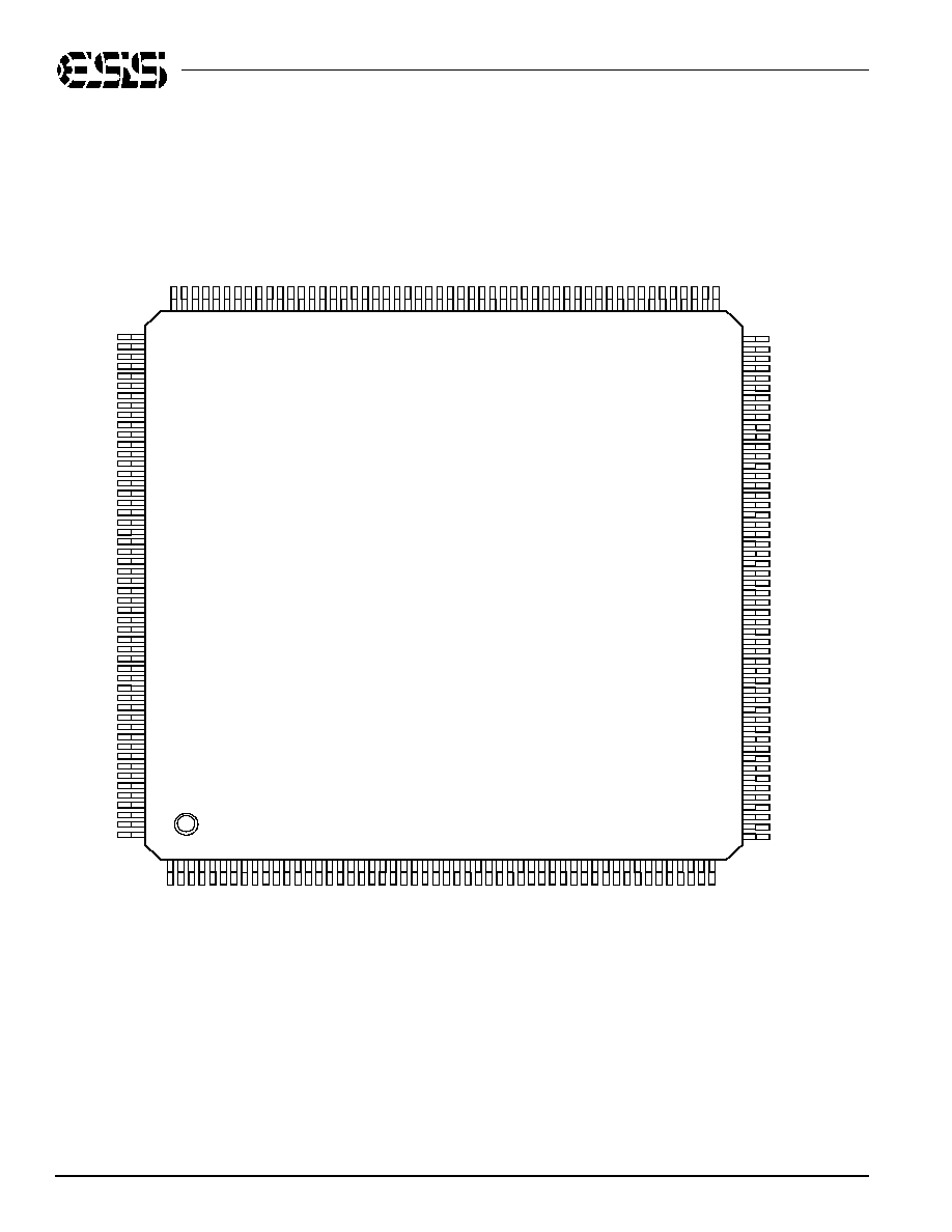
PINOUT
PINOUT
Figure 2 shows the ES4408 device pinout.
Figure 2 ES4408 Device Pinout
1
2
3
4
5
6
7
8
9
10
11
12
13
14
15
16
17
18
19
20
21
22
23
24
25
26
27
28
29
30
31
32
33
34
35
36
37
38
39
40
41
42
43
44
45
46
47
48
49
50
51
52
53
54
55
56
57
58
59
60
61
62
63
64
65
66
67
68
69
70
71
72
73
74
75
76
77
78
79
80
81
82
83
84
85
86
87
88
89
90
91
92
93
94
95
96
97
98
99
100
101
102
103
104
105
106
107
108
109
110
111
112
113
114
115
116
117
118
119
120
121
122
123
124
125
126
127
128
129
130
131
132
133
134
135
136
137
138
139
140
141
142
143
144
145
146
147
148
149
150
151
152
153
154
155
156
157
158
159
160
161
162
163
164
165
166
167
168
169
170
171
172
173
174
175
176
177
178
179
180
181
182
183
184
185
186
187
188
189
190
191
192
193
194
195
196
197
198
199
200
201
202
203
204
205
206
207
208
LCS1#
LOE#
LD0
VSS
LCS3#
LCS2#
AUX0
LA
21
LA
20
RE
SE
T#
VC
C
TS
D3
HI
OC
S1
6
#
HA
1
VS
S
HA
0
HWR
#
HR
D#
HD
4/
DC
I
4
HD
5/
DC
I
5
HD
6/
DC
I
6
HD
2/
DC
I
2
HD
3/
DC
I
3
VC
C
VCC
DB8
VC
C
DB5
DB9
DCS0#
VC
C
VSS
TS
D0
/SE
L_P
LL
0
TS
D1
/SE
L_P
LL
2
TD
MF
S
TD
M
C
LK
TD
MD
R
TD
MT
SC
#
TW
S
/
SE
L_P
LL
1
VC
C
LA
4
LA
5
LA
6
LA
7
LA
8
LA
9
VSS
VC
C
LA
10
LA
1
1
LA
12
LA
13
LA
14
LA
15
LA
16
VSS
VC
C
LA
17
LA
18
LA
19
TD
MD
X/
RS
EL
VSS
TS
D2
SP
DI
F
_
D
O
B
M
NC
VSS
MC
L
K
TB
CK
VCC
VCC
VSS
VSS
DQM
RS
D
RW
S
RB
CK
AP
LLC
AP
XIN
XO
U
T
VC
C
DSCK
VSS
DB15
DB13
DB11
DB1
VSS
DRAS2#
DRAS0#
DOE#/DSCK_EN
VCC
DMA9
DMA7
VSS
DMA5
DMA3
VCC
DCS1#
DB14
DB12
DB10
DB0
VCC
DRAS1#
DWE#
DCAS#
VSS
DMA8
DMA6
VCC
DMA4
DMA2
VSS
DB7
DB6
VSS
DB4
DB3
DB2
DMA11
DMA10
DMA1
DMA0
HC
S3
FX
#
HC
S1
FX
#
VS
S
HI
OR
DY
VS
S
HD
13
HD
12
HD
1
1
HD
10
HD
9
HD
8/
DC
I
_
F
D
S
#
VS
S
HI
RQ
/
D
C
I
_
E
RR
#
HR
ST
#
HR
DQ
#
HWR
Q
#
D
C
I
_R
EQ
#
HD
15
HD
14
VC
C
HD
7/
DC
I
7
HD
1/
DC
I
1
HD
0/
DC
I
0
VC
C
VS
S
HS
YN
CH
#
PC
LK
2X
S
C
N
YU
V7
YU
V6
PC
LK
QS
CN
VS
YN
CH
#
YU
V5
VS
S
VC
C
YU
V4
YU
V3
YU
V2
YU
V1
YU
V0
DC
LK
VC
C
AUX7
AUX6
VCC
LD1
LD2
LA3
LD12
VCC
HA2
VPP
VCC
LD3
LD5
LD9
LD13
LWRHL#
NC
AUX1
AUX3
LD4
LD6
LD10
LD14
VSS
LA0
AUX2
AUX4
VCC
LD7
LD11
LD15
VCC
LA1
VSS
AUX5
VSS
LD8
VSS
LWRLL#
NC
LA2
VSS
VCC
LCS0#
VSS
208-pin PQFP
ES4408
ESS Technology, Inc.
SAM0241-052101
3
ES4408 PRODUCT BRIEF
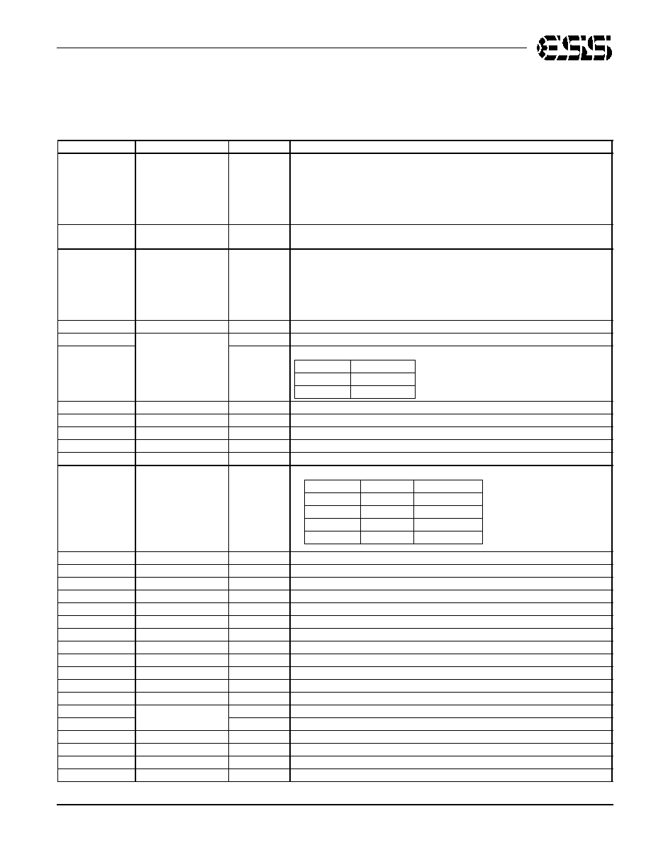
ES4408 PIN DESCRIPTION
ES4408 PIN DESCRIPTION
Table 1 lists the pin descriptions for the ES4408.
Table 1 ES4408 Pin Descriptions
Name
Number
I/O
Definition
VCC
1, 9, 18, 27, 35, 44,
51, 59, 68, 75, 83,
92, 99, 104, 111,
121, 130, 139, 148,
157, 164, 172, 183,
193, 201
I
3.65 V � 150 mv.
LA[21:0]
23:19, 16:10, 7:2,
207:204
O
Device address output.
VSS
8, 17, 26, 34, 43, 52,
60, 67, 76, 84, 91,
98, 103, 112, 120,
129, 138, 147, 156,
163, 171, 177, 184,
192, 200, 208
I
Ground.
RESET#
24
I
Reset input, active low.
TDMDX
25
O
TDM transmit data.
RSEL
I
ROM Select
TDMDR
28
I
TDM receive data.
TDMCLK
29
I
TDM clock input.
TDMFS
30
I
TDM frame sync.
TDMTSC#
31
O
TDM output enable, active low.
TWS
32
O
Audio transmit frame sync.
SEL_PLL[2:0]
33
I
Select PLL1.
TSD[3:0]
38,37,36,33
O
Audio transmit serial data port.
MCLK
39
I/O
Audio master clock for audio DAC.
TBCK
40
I/O
Audio transmit bit clock.
SPDIF_DOBM
41
O
S/PDIF (IEC958) Format Output.
RSD
45
I
Audio receive serial data.
RWS
46
I
Audio receive frame sync.
RBCK
47
I
Audio receive bit clock.
APLLCAP
48
I
Analog PLL Capacitor.
XIN
49
I
Crystal input.
XOUT
50
O
Crystal output.
DMA[11:0]
66:61, 58:53
O
DRAM address bus.
DCAS#
69
O
Column address strobe, active low.
DOE#
70
O
Output enable, active low.
DSCK_EN
I
Clock Enable, active low.
DWE#
71
O
DRAM write enable, active low.
DRAS[2:0]#
74:72
O
Row address strobe, active low.
DB[15:0]
96:93, 90:85, 82:77
I/O
DRAM data bus.
DCS[1:0]#
97,100
O
SDRAM chip select [1:0], active low.
RSEL
Selection
0
8-bit ROM
1
16-bit ROM
SEL_PLL2 SEL_PLL0 Clock Output
0
0
2.5 x DCLK
0
1
3 x DCLK
1
0
3.5 x DCLK
1
1
4 x DCLK
4
SAM0241-052101
ESS Technology, Inc.
ES4408 PRODUCT BRIEF
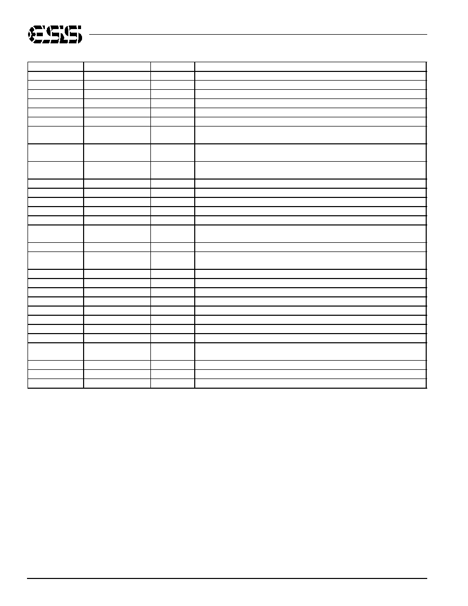
ES4408 PIN DESCRIPTION
Name
Number
I/O
Definition
DQM
101
O
Data input/output mask.
DSCK
102
O
Clock to SDRAM.
DCLK
105
I
Clock Input (27 MHz)
YUV[7:0]
115:113,110:106
O
8-bit YUV output.
PCLK2XSCN
116
I/O
2X pixel clock.
PCLKQSCN
117
I/O
Pixel clock.
VSYNCH#
118
I/O
Vertical sync for screen video interface, programmable for rising or falling
edge, active low.
HSYNCH#
119
I/O
Horizontal sync for screen video interface, programmable for rising or falling
edge, active low.
HD[15:0]
141:140,137:131,12
8:122
O
Host data bus
HCS1FX#
152
O
Host select 1.
HCS3FX#
153
O
Host select 3.
HIOCS16#
151
I
Device 16-bit data transfer.
HA[2:0]
158, 155:154
I/O
Host address bus.
VPP
159
I
5 V power supply.
HWR#/
DCI_ACK#
149
I,O
Host write/DCI Interface Acknowledge Signal, active low.
HRD#/DCI_CLK
150
O,O
Host read/DCI Interface Clock.
HD[15:0]
141:140, 137:131,
128:122
I/O
Host data bus.
HWRQ#
142
O
Host write request.
HRDQ#
143
O
Host read request.
HIRQ
144
I/O
Host interrupt.
HRST#
145
O
Host reset.
HIORDY
146
I
Host I/O ready.
AUX[7:0]
169:165,162:160
I/O
Auxiliary ports.
LOE#
170
O
Device output enable, active low.
LCS[3:0]#
176:173
O
Chip select [3:0], active low.
LD[15:0]
197:194, 191:185,
182:178
I/O
Device data bus.
LWRLL#
198
O
Device write enable, active low.
LWRHL#
199
O
Device write enable, active low.
NC
37,38,42,203:202
--
No connect.
ESS Technology, Inc.
SAM0241-052101
5
ES4408 PRODUCT BRIEF
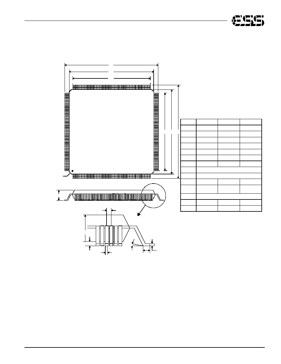
MECHANICAL DIMENSIONS
MECHANICAL DIMENSIONS
Figure 3 shows the mechanical dimensions for the
ES4408.
Figure 3 ES4408 Mechanical Dimensions
see detail
A
E
E1
E3
1
52
157
208
Index
53
104
D
D1
D3
105
Pin 1
Note:
1. All dimensions are in inches (millimeters).
2. Actual package used has millimeter native
dimensions � take care with rounding from metric
to imperial.
Symbol
Min
Nom
Max
A
�
�
0.165
A1
0.010 (0.25)
�
�
A2
0.130 (3.30)
0.134 (3.40)
0.138 (3.50)
B
0.007 (0.18)
0.009 (0.23)
0.011 (0.28)
C
0.005 (0.12)
0.006 (0.16)
0.008 (0.20)
D
1.195 (30.35)
1.205 (30.60)
1.215 (30.85)
D1
1.098 (27.90)
1.102 (28.00)
1.106 (28.10)
D3
1.004 (25.50) REF
e
0.0197 (0.50) BASIC
E
1.195 (30.35)
1.205 (30.60)
1.215(30.85)
E1
1.098 (27.90)
1.102
(28.00)
1.106 (28.10)
E3
1.004 (25.50) REF
L
0.016 (0.40)
0.020 (0.50)
0.024 (0.60)
0 i
2.5 i
5.0 i
e
A1
A2
L
C
B
156