ESS Technology, Inc.
SAM0419-052101 1
ES4408FD
DVD
Processor
Product Brief
DESCRIPTION
The ES4408FD processor provides a single-chip solution
for a Digital Versatile Disc (DVD) player that integrates
MPEG video decoding, DVD system navigation, Content
Scrambling System (CSS) protection, and both DolbyTM
Digital (AC-3), Digital Theater System (DTS), and MPEG
audio decoding. The fully programmable ES4408FD offers
the best feature set in comparison to any currently existing
DVD processor. The ES4408FD includes a glueless
interface to various peripheral components, making it the
most cost effective solution in its class with an integration
level and quality that set new benchmarks.
The ES4408FD DVD processor is capable of decoding
DolbyTM Digital (AC-3), DTS and MPEG audio up to 7.1
channels simultaneously with MPEG-1 or MPEG-2 video.
For embedded applications, the internal 32-bit RISC
processor of the ES4408FD can be used in place of a
microcontroller to provide all system control, DVD system
navigation, CSS decryption, and many other features. On-
chip, multi-tap filters provide arbitrary scaling with state of
the art SmartScaleTM technology useful for video
standards conversion. SmartStreamTM technology from
ESS provides video error concealment and video post-
processing, leading to the highest playability and video
quality. The ES4408FD also supports both letterbox and
pan and scan displays, DVD subpicture overlay, and On-
Screen Display.
The ES4408FD provides a glueless 8/16-bit parallel
interface to many DVD servo/loaders. It connects directly
with 8/16-bit ROM and 16-bit SDRAM/EDO memories. An
8-bit YUV video interface supports many TV encoders.
General purpose auxiliary pins are provided to control
various peripheral devices. A standard I
2
S interface
supports popular audio DACs and ADCs. The ES4408FD
also features a direct S/PDIF output.
The media bitstream from a DVD disc is passed to the
ES4408FD through a 8-bit/16-bit parallel host interface.
The ES4408FD parses the system layer and
demultiplexes the audio and video streams. Audio is
decoded and passed through the I
2
S audio serial bus to an
external audio DAC for audio playback. Video is decoded
and output as YUV pixels to an NTSC or PAL video
encoder. System control and housekeeping functions
(keypad and remote control) are also provided on-chip.
The ES4408FD is available in an industry-standard 208-
pin Plastic Quad Flat Package (PQFP).
FEATURES
�
Single-chip DVD processor in a 208-pin PQFP package
�
Supports MPEG-1 system and MPEG-2 program
streams
�
Programmable multimedia processor architecture
�
Compatible with Audio CD, VideoCD 1.1, 2.0, Interactive
VCD 3.0, and Super VideoCD (SVCD)
�
DVD Navigation 1.0
�
Built-in Content Scrambling System (CSS) protection
�
On-chip DVD Control Interface supports ATAPI and A/V
DVD loaders.
�
On-chip, 4-bit On-Screen Display (OSD) controller
supports standard television remote control functions,
DVD/VCD/SVCD navigation functions and performs 4-bit
pixel blending.
�
On-chip Subpicture Unit (SPU) decoder supports
karaoke lyric, closed captioning and subtitle text display
functions.
�
Supports up to 8 MB of SDRAM
�
Independent audio bit clock for transmit and receive port
�
Single 27 MHz clock input
Video
�
Pan and scan and letterbox widescreen DVD video
display playback modes supported.
�
SmartScaleTM for NTSC to PAL conversion and vice
versa supported.
�
SmartStreamTM for video error concealment supported.
�
SmartZoomTM for motion zoom and pan supported.
�
8-bit YUV output
Audio
�
Karaoke function
�
DolbyTM Digital (AC-3) and DTS S/PDIF digital audio
output
�
DolbyTM Digital (AC-3) and DTS 5.1 channel audio
decoded
�
DolbyTM Digital Class A and DTS certified
�
MPEG audio up to 7.1 channel
�
Linear PCM streams from 48 kHz to 96 KHz
�
Supports 256/384/512 frame sync audio system clock
2
SAM0419-052101
ESS Technology, Inc.
ES4408FD PRODUCT BRIEF
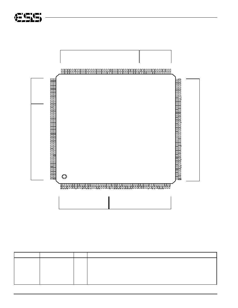
PINOUT
Figure 1 shows the device pinout for the ES4408FD.
Figure 1 ES4408FD Device Pinout
PIN DESCRIPTION
Table 1 lists the pin descriptions for the ES4408FD.
1
2
3
4
5
6
7
8
9
10
11
12
13
14
15
16
17
18
19
20
21
22
23
24
25
26
27
28
29
30
31
32
33
34
35
36
37
38
39
40
41
42
43
44
45
46
47
48
49
50
51
52
53
54
55
56
57
58
59
60
61
62
63
64
65
66
67
68
69
70
71
72
73
74
75
76
77
78
79
80
81
82
83
84
85
86
87
88
89
90
91
92
93
94
95
96
97
98
99
100
101
102
103
104
10
5
10
6
10
7
10
8
10
9
11
0
11
1
11
2
11
3
11
4
11
5
11
6
11
7
11
8
11
9
12
0
12
1
12
2
12
3
12
4
12
5
12
6
12
7
12
8
12
9
13
0
13
1
13
2
13
3
13
4
13
5
13
6
13
7
13
8
13
9
14
0
14
1
14
2
14
3
14
4
14
5
14
6
14
7
14
8
14
9
15
0
15
1
15
2
15
3
15
4
15
5
15
6
157
158
159
160
161
162
163
164
165
166
167
168
169
170
171
172
173
174
175
176
177
178
179
180
181
182
183
184
185
186
187
188
189
190
191
192
193
194
195
196
197
198
199
200
201
202
203
204
205
206
207
208
LCS1#
LOE#
LD0
VSS
LCS3#
LCS2#
AUX0
LA
21
LA
20
RE
S
E
T#
VC
C
TS
D3
HIO
C
S
1
6
#
HA
1
VS
S
HA
0
HW
R#
HRD
#
HD4
/DCI
4
HD5
/DCI
5
HD6
/DCI
6
HD2
/DCI
2
HD3
/DCI
3
VC
C
VCC
DB8
VC
C
DB5
DB9
DCS0#
VC
C
VSS
T
S
D
0
/
S
EL
_P
LL
0
T
S
D
1
/
S
EL
_P
LL
2
TDM
F
S
TDM
C
L
K
TDM
D
R
TD
M
T
S
C
#
T
W
S
/
SE
L_
PL
L1
VC
C
LA
4
LA
5
LA
6
LA
7
LA
8
LA
9
VSS
VC
C
LA
10
LA
1
1
LA
12
LA
13
LA
14
LA
15
LA
16
VSS
VC
C
LA
17
LA
18
LA
19
TDM
D
X
/
R
S
E
L
VSS
TS
D2
S
P
D
IF
_DO
B
M/
PL
L3
NC
VSS
MC
LK
TB
C
K
VCC
VCC
VSS
VSS
DQM
RS
D
RW
S
RB
CK
AP
LL
C
A
P
XI
N
XO
U
T
VC
C
DSCK
VSS
DB15
DB13
DB11
DB1
VSS
DRAS2#
DRAS0#
DOE#/DSCK_EN
VCC
DMA9
DMA7
VSS
DMA5
DMA3
VCC
DCS1#
DB14
DB12
DB10
DB0
VCC
DRAS1#
DWE#
DCAS#
VSS
DMA8
DMA6
VCC
DMA4
DMA2
VSS
DB7
DB6
VSS
DB4
DB3
DB2
DMA11
DMA10
DMA1
DMA0
HCS
3FX
#
HCS
1FX
#
VS
S
HIO
R
D
Y
VS
S
HD1
3
HD1
2
HD1
1
HD1
0
HD9
HD8
/DCI
_FDS
#
VS
S
HIR
Q
/
DCI_
E
RR
#
HRS
T#
HRD
Q
#
HW
RQ
#D
CI_R
E
Q
#
HD1
5
HD1
4
VC
C
HD7
/DCI
7
HD1
/DCI
1
HD0
/DCI
0
VC
C
VS
S
HS
Y
N
C#
P
C
LK
2X
SCN
YU
V
7
YU
V
6
PC
L
K
Q
S
C
N
VS
YN
C
#
YU
V
5
VS
S
VC
C
YU
V
4
YU
V
3
YU
V
2
YU
V
1
YU
V
0
DCL
K
VC
C
AUX7
AUX6
VCC
LD1
LD2
LA3
LD12
VCC
HA2
VPP
VCC
LD3
LD5
LD9
LD13
LWRHL#
NC
AUX1
AUX3
LD4
LD6
LD10
LD14
VSS
LA0
AUX2
AUX4
VCC
LD7
LD11
LD15
VCC
LA1
VSS
AUX5
VSS
LD8
VSS
LWRLL#
NC
LA2
VSS
VCC
LCS0#
VSS
208-Pin PQFP Package
ES4408FD
Video Interface
Host / ATAPI / DCI Interface
Auxiliary
Interface
RISC
Interface
RISC
Interface
Audio/TDM
Interface
Memory
Interface
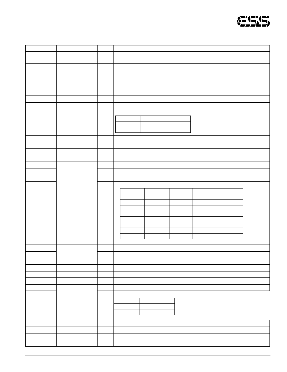
Table 1 ES4408FD Pin Descriptions
Name
Number
I/O
Definition
VCC
1, 9, 18, 27, 35, 44,
51, 59, 68, 75, 83,
92, 99, 104, 111,
121, 130, 139, 148,
157, 164, 172, 183,
193, 201
I
Supply voltage.
ESS Technology, Inc.
SAM0419-052101
3
ES4408FD PRODUCT BRIEF
Name
Number
I/O
Definition
LA[21:0]
23:19,16:10,7:2,
207:204
O
Device address output.
VSS
8, 17, 26, 34, 43, 52,
60, 67, 76, 84, 91,
98, 103, 112, 120,
129, 138, 147, 156,
163, 171, 177, 184,
192, 200, 208
I
Ground.
RESET#
24
I
Reset input, active low.
TDMDX
25
O
TDM transmit data.
RSEL
I
ROM Select
TDMDR
28
I
TDM receive data.
TDMCLK
29
I
TDM clock input.
TDMFS
30
I
TDM frame sync.
TDMTSC#
31
O
TDM output enable, active low.
TWS
32
O
Audio transmit frame sync.
SEL_PLL2
I
Select PLL2 input.
TSD[0]
33
O
Audio transmit serial data output 0.
SEL_PLL 0
I
Select PLL0 input.
TSD[1]
36
O
Audio transmit serial data output 1.
SEL_PLL1
I
Select PLL1 input
TSD[2]
37
O
Audio transmit serial data output 2.
TSD[3]
38
O
Audio transmit serial data output 3.
MCLK
39
I/O
Audio master clock for audio DAC.
TBCK
40
I/O
Audio transmit bit clock.
SPDIF_DOBM
41
O
S/PDIF (IEC958) Format Output.
SEL_PLL3
I
Clock Source Select.
RSD
45
I
Audio receive serial data.
RWS
46
I
Audio receive frame sync.
RBCK
47
I
Audio receive bit clock.
APLLCAP
48
I
Analog PLL Capacitor.
Table 1 ES4408FD Pin Descriptions (Continued)
RSEL
Selection
0
16-bit ROM
1
8-bit ROM
SEL_PLL2 SEL_PLL1 SEL_PLL0 Clock Output
0
0
0
VCO Off
0
0
1
27.0 MHz
0
1
0
Bypass
0
1
1
54.0 MHz
1
0
0
121.5 MHz
1
0
1
81.0 MHz
1
1
0
94.0 MHz
1
1
1
108.0 MHz
SEL_PLL3 Clock Source
0
Crystal oscillator
1
DCLK input

4
SAM0419-052101
ESS Technology, Inc.
ES4408FD PRODUCT BRIEF
Name
Number
I/O
Definition
XIN
49
I
Crystal input.
XOUT
50
O
Crystal output.
DMA[11:0]
66:61,58:53
O
DRAM address bus.
DCAS#
69
O
DRAM Column address strobe, active low.
DOE#
70
O
DRAM Output enable, active low.
DSCK_EN
I
DRAM Clock Enable, active low.
DWE#
71
O
DRAM write enable, active low.
DRAS[2:0]#
74:72
O
DRAM Row address strobe, active low.
DB[15:0]
96:93,90:85,82:77
I/O
DRAM data bus.
DCS[1:0]#
97,100
O
SDRAM chip select [1:0], active low.
DQM
101
O
Data input/output mask.
DSCK
102
O
Clock to SDRAM.
DCLK
105
I
Clock Input (27 MHz)
YUV[7:0]
115:113,110:106
O
8-bit YUV output.
PCLK2XSCN
116
I/O
Doubled screen 27-MHz pixel clock.
PCLKQSCN
117
I/O
Screen Pixel clock.
VSYNC#
118
I/O
Vertical sync for video display interface, programmable for rising or falling edge,
active low.
HSYNC#
119
I/O
Horizontal sync for screen video interface, programmable for rising or falling edge,
active low.
HD[15:0]
141:140,137:131,
128:122
O
Host data bus
HCS1FX#
152
O
Host select 1.
HCS3FX#
153
O
Host select 3.
HIOCS16#
151
I
Device 16-bit data transfer.
HA[2:0]
158, 155:154
I/O
Host address bus.
VPP
159
I
Peripheral protection voltage.
HWR#/
DCI_ACK#
149
I,O
Host write/DCI Interface Acknowledge Signal, active low.
HRD#/
DCI_CLK
150
O,O
Host read/DCI Interface Clock.
HWRQ#
142
O
Host write request.
HRDQ#
143
O
Host read request.
HIRQ
144
I/O
Host interrupt.
HRST#
145
O
Host reset.
HIORDY
146
I
Host I/O ready.
AUX[7:0]
169:165,162:160
I/O
Auxiliary ports.
LOE#
170
O
Device output enable, active low.
LCS[3:0]#
176:173
O
Chip select [3:0], active low.
LD[15:0]
197:194, 191:185,
182:178
I/O
Device data bus.
LWRLL#
198
O
Device write enable, active low.
LWRHL#
199
O
Device write enable, active low.
NC
37,38,42,203:202
--
No connect pins. Leave open.
Table 1 ES4408FD Pin Descriptions (Continued)
ESS Technology, Inc.
SAM0419-052101
5
ES4408FD PRODUCT BRIEF
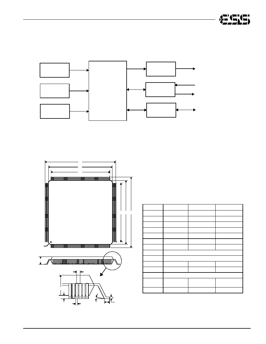
SYSTEM BLOCK DIAGRAM
Figure 2 shows a sample system block diagram using the
ES4408FD.
Figure 2 ES4408FD System Block Diagram
MECHANICAL DIMENSIONS
Figure 3 shows the mechanical dimensions of the ES4408FD.
Figure 3 ES4408FD Mechanical Dimensions
ES4408FD
8MB EDO
or SDRAM
DVD drive
EPROM
Panel
Interface
NTSC/PAL
Encoder
Audio
CODEC
TV
MIC
Speakers
Remote Control/
Keypad
Video
Audio
see detail
A
E
E1
E3
1
52
157
208
Index
53
104
D
D1
D3
105
Pin 1
Note:
1. All dimensions are in inches (millimeters).
2. Actual package used has millimeter native dimensions � take care with
rounding from metric to imperial.
Symbol
Min
Nom
Max
A
�
�
0.165
A1
0.010 (0.25)
�
�
A2
0.130 (3.30)
0.134 (3.40)
0.138 (3.50)
B
0.007 (0.18)
0.009 (0.23)
0.011 (0.28)
C
0.005 (0.12)
0.006 (0.16)
0.008 (0.20)
D
1.195 (30.35)
1.205 (30.60)
1.215 (30.85)
D1
1.098 (27.90)
1.102 (28.00)
1.106 (28.10)
D3
1.004 (25.50) REF
e
0.0197 (0.50) BASIC
E
1.195 (30.35)
1.205 (30.60)
1.215 (30.85)
E1
1.098 (27.90)
1.102 (28.00)
1.106 (28.10)
E3
1.004 (25.50) REF
L
0.016
(0.40)
0.020
(0.50)
0.024
(0.60)
f
0 i
2.5 i
5.0 i
e
A1
A2
L
C
B
156