 | ÐлекÑÑоннÑй компоненÑ: 198A854 | СкаÑаÑÑ:  PDF PDF  ZIP ZIP |
0038_128kx72x2_sram.PDF
128K x 72 x 2
Radiation Hardened
Static RAM MCM 3.3 V
198A854
BAE SYSTEMS · 9300 Wellington Road · Manassas, Virginia 20110-4122
Product Description
Radiation
· Fabricated with Bulk CMOS 0.5 µm Process
· Total Dose Hardness through 1x10
6
rad(Si)
· Neutron Hardness through 1x10
14
N/cm
2
· Dynamic and Static Transient Upset Hardness
through 1x10
9
rad(Si)/s
· Soft Error Rate of < 1x10
-11
Upsets/Bit-Day
· Dose Rate Survivability through 1x10
12
rad(Si)/s
· Latchup Free
Features
Other
· Read/Write Cycle Times
50 ns (-30 °C to 90°C)
· SMD Number Pending
· Asynchronous Operation
· CMOS or TTL Compatible I/O
· Single 3.3 V ± 5% Power Supply
· Low Operating Power
· Packaging Options
· 308-Lead Quad Flat Pack (2.050" x 2.050")
General Description
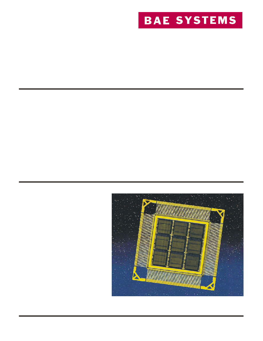
The 128K x 72 x 2 radiation hardened static
RAM is composed of 18 128K x 8 SRAM
memory die assembled in a single, double-
sided ceramic substrate. Each die is a high
performance 131,072 word x 8-bit static
random access memory with industry-
standard functionality. It is fabricated with
BAE SYSTEMS' radiation hardened
technology and is designed for use in
systems operating in radiation
environments. The RAM operates over the
full military temperature range and requires
a single 3.3 V ± 5% power supply. The RAM
is available with TTL or CMOS compatible
I/O. Power consumption is less than 162
mW/MHz in operation, and less than 90 mW
in the low power disabled mode. The RAM
read operation is fully asynchronous, with an
associated typical access time of 35
nanoseconds.
BAE SYSTEMS' enhanced bulk CMOS
technology is radiation hardened through
the use of advanced and proprietary design,
layout, and process hardening techniques.
2
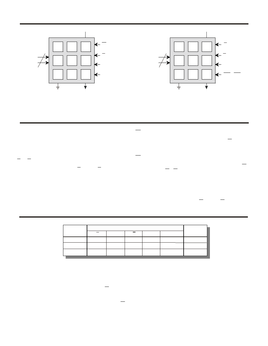
Functional Diagram
Signal Definitions
A: 0-16
DQ: 0-71
S1 - S18
Address input pins that select a particular
eight-bit word within the memory array.
Bi-directional data pins that serve as data
outputs during a read operation and as
data inputs during a write operation.
Negative chip select, when at a low level,
allows normal read or write operation.
When at a high level, S1 through S18
forces the SRAM to a precharge condition,
holds the data output drivers in a high
impedance state and disables the data
input buffers only. If this signal is not used,
it must be connected to GND.
Negative write enable, when at a low level, activates a
write operation and holds the data output drivers in a
high impedance state. When at a high level, W allows
normal read operation.
Negative output enable, when at a high level holds the
data output drivers in a high impedance state. When at
a low level, the data output driver state is defined by S1
through S18, W and E1 through E18. If this signal is not
used it must be connected to GND.
Chip enable, when at a high level allows normal
operation. When at a low level, E1 through E18 forces
the SRAM to a precharge condition, holds the data
output drivers in a high impedance state and disables all
the input buffers except the S1 through S18 input buffer.
If this signal is not used, it must be connected to V
DD
.
W
G
E1 - E18
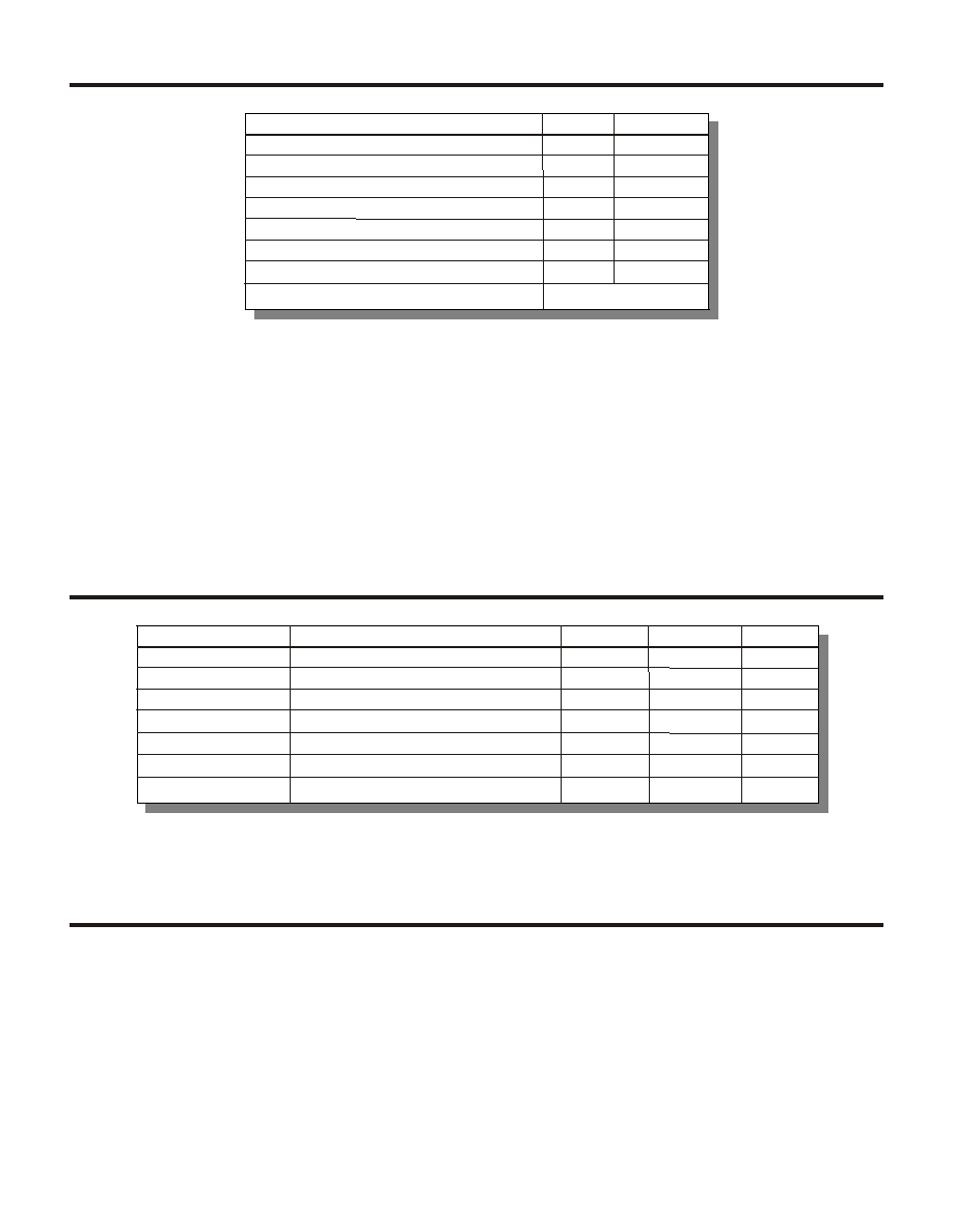
Truth Table
Notes:
1) V
IN
for don't care (X) inputs = V
IL
or V
IH
.
2) When G = high, I/O is high-Z.
3) To dissipate the minimum amount of standby power when in
standby mode: S1 = V
DD
. All other input levels may float.
W Top
G Top
E1 - E9
(for U0 to U8)
Top
A0 to A16
Top
72 Data I/O
Top
GND
Top
Lead 1
S1 - S9
(for U0 to U8)
U6
U0
U3
U7
U1
U4
U8
U2
U5
W Bottom
G Bottom
E10 - E18
(for U9 to U17)
Bottom
A0 to A16
Bottom
72 Data I/O
Bottom
GND
Bottom
Lead 1
S10 - S18
(for U9 to U17)
U15
U9
U12
U16
U10
U13
U17
U11
U14
Top and
Bottom
Top and
Bottom
Top and
Bottom
Mode
Inputs
(1),(2)
E
High
Low
High
W
Low
High
X
G
X
Low
X
I/O
Data-In
Data-Out
High-Z
Power
Active
Active
Standby
Write
Read
Standby
(3)
S
Low
Low
High
V
DD
Bottom
V
DD
Top
3
Notes:
The substrate of this module is connected directly to Ground.
Power shall be applied to the device only in the following
sequences to prevent damage due to excessive currents:
· Power-Up Sequence: GND, V
DD
, Inputs
· Power-Down Sequence: Inputs, V
DD
, GND
Absolute Maximum Ratings
Recommended Operating Conditions
Power Sequencing
1)All voltages referenced to GND.
Note:
1) Stresses above the absolute maximum rating may cause permanent
damage to the device. Extended operation at the maximum levels may
degrade performance and affect reliability. All voltages are with
reference to the module ground leads.
2) Maximum applied voltage shall not exceed +5.5 V.
3) Guaranteed by design; not tested.
4) Class as defined in MIL-STD-883, Method 3015.
Minimum
-65°C
-30°C
-0.5 V
-0.5 V
-0.5 V
(Class I)
Storage Temperature Range (Ambient)
Applied Conditions
(1)
Operating Temperature Range (T
CASE
)
Positive Supply Voltage
Input Voltage
(2)
Output Voltage
(2)
Power Dissipation
(3)
Lead Temperature (Soldering 5 sec)
Electrostatic Discharge Sensitivity
(4)
Maximum
+150°C
+105°C
+5.5 V
V
DD
+ 0.5 V
4.04 W
+250°C
V
DD
+ 0.5 V
Minimum
+3.14
0.0
-30
Units
Volt
Volt
Celsius
Supply Voltage
Parameters
(1)
Supply Voltage Reference
Case Temperature
Symbol
V
DD
GND
T
C
Maximum
+3.46
0.0
+90
0.0
+2.0
Volt
Volt
Input Logic "Low" (Data)
Input Logic "High" (Data)
V
IL
Data
V
IH
Data
+1.0
V
DD
0.0
+2.0
Volt
Volt
Input Logic "Low" (Address and Clocks)
Input Logic "High" (Address and Clocks)
V
IL
Address and Clock
V
IH
Address and Clock
+1.0
V
DD
4
1) Typical operating conditions: -30°C
T
case
+105°C; 3.14 V
V
DD
3.46 V;
unless otherwise specified.
2) Limit specified at T
case
= 80°C. Guaranteed, but not tested.
3) Guaranteed by design and verified by periodic characterization
167 ± 10%
1.73 V
50 pF + 10%
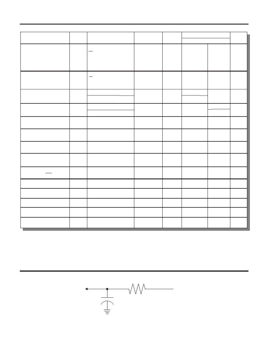
Output Load Circuit
DC Electrical Characteristics
Note:
Symbol Test Conditions
(1)
Device
Type
Limits
Minimum
Maximum
Units
I
DD1
V
OH
I
OH
= -200 µA
I
OH
= -4 mA
I
OL
= 200 µA
I
OL
= 8 mA
All
All
All
All
All
All
All
3240
54
2.4
-90
-60
0.4
V
DD
- 0.5 V
0.05
90
60
15
mA
mA
µA
µA
pF
V
V
Test
Supply Current
(Cycling Selected)
Supply Current
(Standby)
Input Leakage Address,
CE, CS, OE, WE
Output Leakage
C
DATA I/O
Data In/Data Out
High Level Output Voltage
Low Level Output Voltage
I
DD3
(2)
V
OL
I
OLK
0 V
V
OUT
3.47 V
Group A
Sub-Groups
1, 2, 3
1, 2, 3
1, 2, 3
1, 2, 3
1, 2, 3
1, 2, 3
All
100
pF
C
in
Address Lines
(3)
(2)
F = F
MAX
= 1/t
AVAV(min)
No Output Load
S = V
IL
= GND
E = V
IH
= V
DD
F = 0 MHz
S = V
IH
= V
DD
E = V
IL
= GND
All
2.2
V
High Level Input Voltage
Data I/O
V
IH_DI/O
1, 2, 3
All
V
Low Level Input Voltage
Data I/O
V
IL_DI/O
1, 2, 3
0.8
All
2.2
V
High Level Input Voltage
Address and Clocks
V
IH
1, 2, 3
All
V
Low Level Input Voltage
Address and Clocks
V
IL
1, 2, 3
0.8
V
DD
All
15
pF
C
in
G, E, S
(3)
All
75
pF
C
in
W
(3)
Notes:
1) Test conditions: input switching levels V
IL
/V
IH
= 0.5 V/V
DD
-0.5 V (CMOS), V
IL
/V
IH
= 0V/3 V (TTL),
input rise and fall times < 5 ns, input and output timing reference levels shown in the Tester AC
Timing Characteristics table, capacitive output loading C
L
= 50 pF. For C
L
> 50 pF, derate
access times by 0.02 ns/pF (typical). -30 °C
T
case
+90°C; 3.14 V
V
DD
3.46 V; unless
otherwise specified.
2) Cycle time per individual die.
5
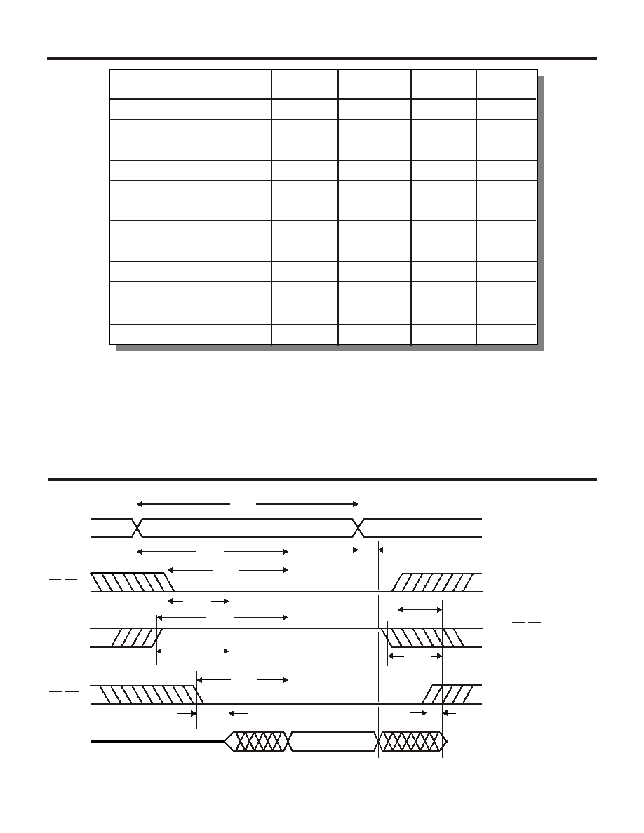
Read Cycle AC Timing Characteristics
(1)
Read Cycle Timing Diagram
Units
Test
Minimum or
Maximum
Symbol
Limits
ns
Chip Select to Output Active
Minimum
t
SLQX
0
ns
Chip Enable to Output Active
Minimum
t
EHQX
0
ns
Output Hold After Address Change
Minimum
t
AXQX
0
ns
Chip Select to Output Disable
Maximum
t
SHQZ
20
ns
Output Enable to Output Active
Minimum
t
GHQZ
0
ns
Read Cycle Time
Minimum
t
AVAV
(2)
50
ns
Address Access Time
Maximum
t
AVQV
50
ns
Chip Select Access Time
Maximum
t
SLQV
50
ns
Chip Enable Access Time
Maximum
t
EHQV
50
ns
Chip Disable to Output Disable
Maximum
t
ELQZ
20
ns
Output Enable Access Time
Maximum
t
GLQV
40
ns
Output Enable to Output Disable
Maximum
t
GHQZ
20
Note:
1) S1/SN, E1/EN,
G1/GN respectively
represent one of
18 clock inputs.
t
ELQZ
t
AVAV
Valid Address
Valid Data
High Impedance
Address
Top or
Bottom
t
AVQV
t
SLQV
t
SLQX
t
EHQV
t
EHQX
t
GLQV
t
GLQX
E1/EN
S1/SN
G1/GN
Data Out
Top or
Bottom
t
GHQZ
t
SHQZ
t
AXQX