
STS20NHS3LL
2/9
Table 3: Absolute Maximum ratings
Table 4: Thermal Data
Table 5: Avalanche Characteristics
ELECTRICAL CHARACTERISTICS (T
J
=25∞C UNLESS OTHERWISE SPECIFIED)
Table 6: On /Off
Table 7: Dynamic
Symbol
Parameter
Value
Unit
V
DS
Drain-source Voltage (V
GS
= 0)
30
V
V
GS
Gate- source Voltage
± 18
V
I
D(1)
Drain Current (continuous) at T
C
= 25∞C
20
A
I
D
Drain Current (continuous) at T
C
= 100∞C
12.6
A
I
DM
(2)
Drain Current (pulsed)
80
A
P
tot
Total Dissipation at T
C
= 25∞C
2.7
W
Rthj-amb (3)
T
j
T
stg
Thermal Resistance Junction-ambient Max
Maximum Operating Junction Temperature
Storage Temperature
47
-55 to 150
-55 to 150
∞C/W
∞C
∞C
Symbol
Parameter
Max Value
Unit
I
AV
Not-Repetitive Avalanche Current
(pulse width limited by T
j
max)
12.5
A
E
AS
Single Pulse Avalanche Energy
(starting T
j
= 25∞C, I
D
= I
AV
, V
DD
= 24V)
1.3
J
Symbol
Parameter
Test Conditions
Min.
Typ.
Max.
Unit
V
(BR)DSS
Drain-source
Breakdown Voltage
I
D
= 1mA, V
GS
= 0
30
V
I
DSS
Zero Gate Voltage
Drain Current (V
GS
= 0)
V
DS
= 24V
500
µA
I
GSS
Gate-body Leakage
Current (V
DS
= 0)
V
GS
= ± 18V
±100
nA
V
GS(th)
Gate Threshold Voltage
V
DS
= V
GS
, I
D
= 1mA
1
2.5
V
R
DS(on)
Static Drain-source On
Resistance
V
GS
= 10V, I
D
= 10A
V
GS
= 4.5V, I
D
= 10A
0.0032
0.004
0.004
0.0055
Symbol
Parameter
Test Conditions
Min.
Typ.
Max.
Unit
g
fs
(4)
Forward Transconductance
V
DS
=15V, I
D
= 12A
30
S
C
iss
C
oss
C
rss
Input Capacitance
Output Capacitance
Reverse Transfer
Capacitance
V
DS
= 25V, f = 1MHz,
V
GS
= 0
3950
720
70
pF
pF
pF

3/9
STS20NHS3LL
ELECTRICAL CHARACTERISTICS (CONTINUED)
Table 8: Switching On
Table 9: Switching Off
Table 10: Source Drain Diode
Notes:
1. This value is rated according to Rthj-pcb
2. Pulse width limited by safe operating area
3. When mounted on FR-4 board with 1 inch
2
pad, 2 oz of Cu and t
<
10sec
4. Pulsed: pulse duration = 300µs, duty cycle 1.5%
Symbol
Parameter
Test Conditions
Min.
Typ.
Max.
Unit
t
d(on)
t
r
Turn-on Delay Time
Rise Time
V
DD
= 15V, I
D
= 10A
R
G
= 4.7
, V
GS
= 4.5V
(see Figure 15)
TBD
TBD
ns
ns
Q
g
Q
gs
Q
gd
Total Gate Charge
Gate-Source Charge
Gate-Drain Charge
V
DD
=15V, I
D
=20A
V
GS
= 4.5V
(see Figure 17)
27.5
7.9
8.7
37
nC
nC
nC
Symbol
Parameter
Test Conditions
Min.
Typ.
Max.
Unit
t
d(off)
t
f
Turn-off Delay Time
Fall Time
V
DD
= 15V, I
D
= 10A
R
G
= 4.7
,
V
GS
= 4.5V
(see Figure 15)
TBD
TBD
ns
ns
Symbol
Parameter
Test Conditions
Min.
Typ.
Max.
Unit
I
SD
I
SDM
Source-drain Current
Source-drain Current (pulsed)
20
80
A
A
V
SD
(
4
)
Forward On Voltage
I
SD
= 10A ,V
GS
= 0
0.7
V
t
rr
Q
rr
I
RRM
Reverse Recovery Time
Reverse Recovery Charge
Reverse Recovery Current
I
SD
= 10A, di/dt = 100A/µs
V
DD
= 25V, T
j
= 150∞C
(see Figure 16)
1.9
26
25
ns
nC
A
STS20NHS3LL
4/9
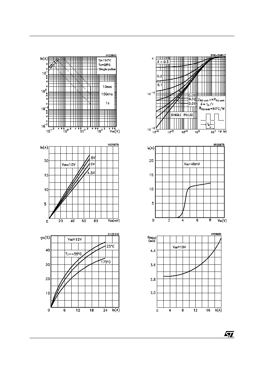
Figure 3: Safe Operating Area
Figure 4: Output Characteristics
Figure 5: Transconductance
Figure 6: Thermal Impedance
Figure 7: Transfer Characteristics
Figure 8: Static Drain-source On Resistance
5/9
STS20NHS3LL
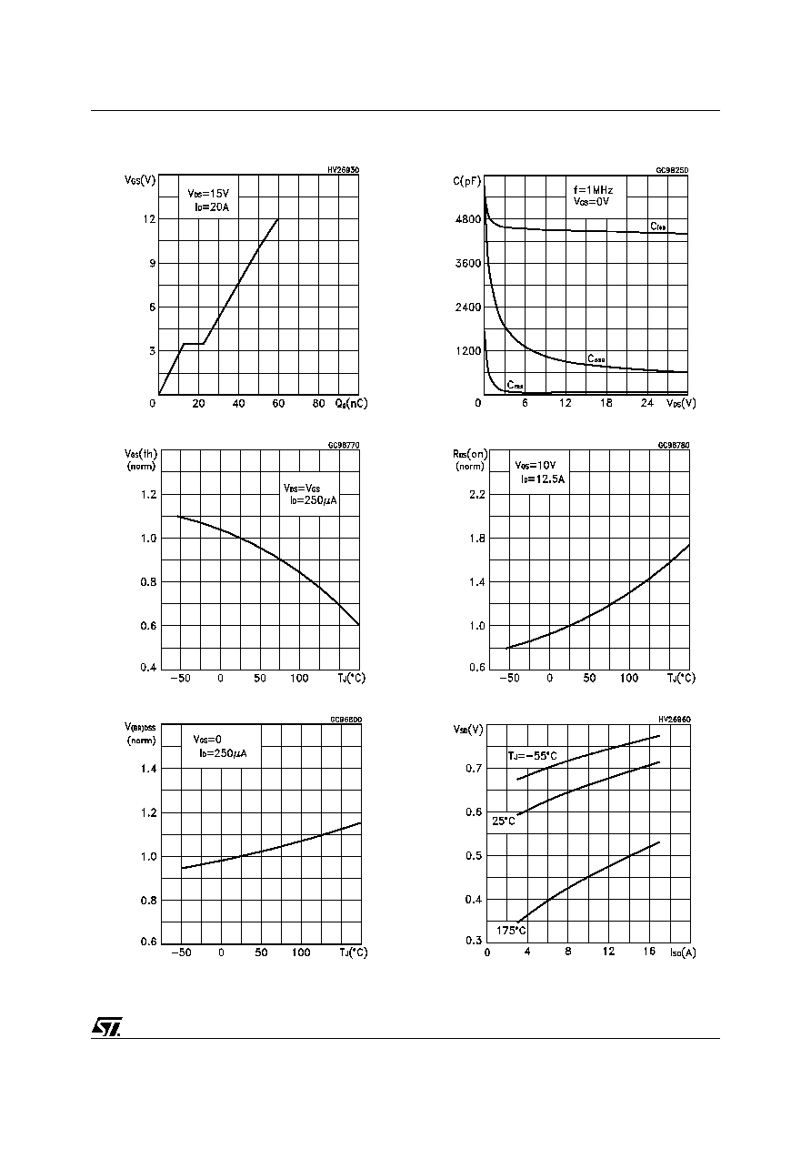
Figure 9: Gate Charge vs Gate-source Voltage
Figure 10: Normalized Gate Thereshold Volt-
age vs Temperature
Figure 11: Normalized On Resistance vs Tem-
perature
Figure 12: Capacitance Variations
Figure 13: Normalized BVDSS vs Temperature
Figure 14: Source-Drain Diode Forward Char-
acteristics

STS20NHS3LL
6/9
Figure 15: Switching Times Test Circuit For
Resistive Load
Figure 16: Test Circuit For Diode Recovery
Times
Figure 17: Gate Charge Test Circuit