 | –≠–ª–µ–∫—Ç—Ä–æ–Ω–Ω—ã–π –∫–æ–º–ø–æ–Ω–µ–Ω—Ç: 238A790 | –°–∫–∞—á–∞—Ç—å:  PDF PDF  ZIP ZIP |
32K x 8
Radiation Hardened Programmable
Read Only Memory (PROM) ≠ 3.3V
238A790
BAE SYSTEMS ∑ 9300 Wellington Road ∑ Manassas, Virginia 20110-4122
Product Description
Radiation
∑ Fabricated with Bulk CMOS 0.8 µm Process
∑ Total Dose Hardness through 2x10
5
rad(Si)
∑ Neutron Hardness through 1x10
12
N/cm
2
∑ SEU Immune (No Latches)
∑ Latchup Free
Features
Other
∑ Read/Write Cycle Times
100 ns (-55 ∞C to 125∞C)
∑ SMD Number Pending
∑ Asynchronous Operation
∑ TTL Compatible I/O
∑ Single 3.3 V ±5% Power Supply
∑ Low Operating Power
∑ Packaging Options
∑ 28-Lead Flat Pack (0.500" x 0.720")
General Description
The 32K x 8 radiation hardened PROM is
pinout, function and package compatible with
commercial 28C256 series 32K x 8 EEPROMs,
such as SEEQ 28C256 and Atmel AT28C256.
The PROM is fabricated with BAE SYSTEMS'
QML-qualified radiation hardened technology,
and is designed for use in systems operating in
radiation environments.
The radiation hardened
Oxide-Nitride-Oxide (ONO) anti-fuse technology
features 0.8 micron, 5 V transistors in the data
path, and 1.0 micron, high voltage N and PFETs
in the programming path circuitry. The PROM
operates over the full military temperature
range, requires a single 3.3 V ± 5% power
supply, and is available with TTL compatible
I/O. Power consumption is typically 15
mW/MHz in operation and is less than 10
mW/MHz in the low power disabled mode. The
PROM operation is fully asynchronous, with an
associated typical access time of 100
nanoseconds. Synchronous operation is also
possible using CE as a clock.
BAE SYSTEMS' enhanced bulk CMOS
technology is radiation hardened through the
use of advanced and proprietary design, layout,
and process hardening techniques.
2
Functional Diagram
Signal Definitions
A: 0-14
DQ: 0-7
OE
≠ Address input pins that select a particular
eight-bit word within the memory array.
≠ Bi-directional data pins that serve as data
outputs during a read operation and as data
inputs during a write operation.
≠ Negative output enable, when at a high level,
holds the data output drivers in a high
impedance state. In programming mode, with
OE high and CE low, data driver state is in
"Data-In" to enable programming.
≠ Chip enable, when at a low level with OE at low
level, allows normal operation. When at a high
level, CE forces the data output drivers in a high
impedance state.
CE
Truth Table
*PROM Programming Voltage
Column Decoders
Section Select
Control Logic
Row Decoders
I/O Buffers
Memory Array
Column Muxing
and
Sense Amps
A0 - A4
DQ0 - 7
A12 - A14
OE
CE
VPP*
A5 - A11
Mode
Inputs
(1),(2)
Power
(3)
Active
Active
Standby1
Standby2
High
CE
Low
Low
V
DD
Low
OE
Low
High
X
X
High
VPP
V
DD
V
DD
V
DD
V
DD
17V ± 0.5V
I/O
Data-Out
High-Z
High-Z
High-Z
Data-In
Programming
Standby
Read
Tristate
Standby
Program
(4)
Notes:
1) V
IN
for don't care (X) inputs = V
IL
or V
IH
.
2) High: V
IN
2.2 V for TTL inputs.
Low: V
IN
0.8 V for TTL inputs.
3) Minimum I
DD
is drawn when standby mode is implemented with
CE = V
DD
(standby1 power).
4) Programming needs to be done using V
DD
= 5V.
3
Notes:
Notes:
1) All voltages referenced to GND.
2) V
PP
= V
DD
during non-programming mode.
Power shall be applied to the device only in the following
sequences to prevent damage due to excessive currents:
∑ Power-Up Sequence: GND, V
DD
, Inputs
∑ Power-Down Sequence: Inputs, V
DD
, GND
Absolute Maximum Ratings
Recommended Operating Conditions
Power Sequencing
Minimum
-65∞C
-55∞C
-0.5 V
-0.5 V
-0.5 V
(Class I)
Storage Temperature Range (Ambient)
Applied Conditions
(1)
Operating Temperature Range
Positive Supply Voltage
Input Voltage
(2)
Output Voltage
(2)
Power Dissipation
(3)
Lead Temperature (Soldering 5 sec)
Electrostatic Discharge Sensitivity
(4)
Maximum
+150∞C
+125∞C
+7.0 V
V
DD
+ 0.5 V
1.5 W
+250∞C
V
DD
+ 0.5 V
1) Stresses above the absolute maximum rating may cause permanent
damage to the device. Extended operation at the maximum levels may
degrade performance and affect reliability. All voltages are with
reference to the module ground leads.
2) Maximum applied voltage shall not exceed +7.0 V.
3) Guaranteed by design; not tested.
4) Class as defined in MIL-STD-883, Method 3015.
Minimum
0.0
-55
0.0
+2.2
Units
Volt
Celsius
Volt
Volt
Parameters
(1)
Supply Voltage Reference
Case Temperature
Input Logic "Low" - TTL
Input Logic "High" - TTL
Symbol
GND
T
C
V
IL
V
IH
Maximum
+3.14
Volt
Supply Voltage
V
DD
+3.46
0.0
+125
+0.8
V
DD
V
DD
(2)
Volt
Programming Voltage
V
PP
V
DD
(2)
4
1) -55 ∞C
T
case
+125∞C; 3.14 V
V
DD
3.46 V; unless otherwise
specified.
Test conditions for AC measurements:
167 ± 10%
1.73V
50 pF ± 10%
Output Load Circuit
DC Electrical Characteristics
Note:
Symbol
Test Conditions
(1)
Limits
Minimum
Maximum
Units
I
DD1
V
OH
0 V
V
IN
5.5 V
-5
-10
5
10
7
10
150
mA
µA
µA
pF
pF
V
V
Test
Supply Current
(Cycling Selected)
Supply Current
(Standby)
Input Leakage
Output Leakage
C
in
C
out
High Level Output Voltage
Low Level Output Voltage
0.4
0.1
I
OH
= -200 µA
I
OH
= -2 mA
I
OL
= 200 µA
I
OL
= 4 mA
2.4
V
DD
- 0.1 V
I
DD2
V
OL
I
ILK
I
OLK
F = F
MAX
= 1/t
AVAV(min)
CE = V
PP
= V
IH
= V
DD
0 V
V
OUT
5.5 V
2.2
0.8
V
V
High Level Input Voltage
TTL Inputs
Low Level Input Voltage
TTL Inputs
V
IH
V
IL
2.0
mA
F = F
MAX
= 1/t
AVAV(min)
No Output Load
CMOS Input
Device
Type
(2)
All
All
All
All
All
All
All
All
All
All
Group A
Subgroups
1, 2, 3
1, 2, 3
4
4
1, 2, 3
1, 2, 3
1, 2, 3
1, 2, 3
1, 2, 3
1, 2, 3
2) Measured during initial device characterization.
0 V to V
DD
2.0 ns/Volt
1.5 V
V
OL
= 1.23 V;
V
OH
= 2.23 V
50%
See Output Load Circuit
Diagram
See Read Cycle Timing
∑ Input Levels
∑ Input Rise and Fall Time
∑ Input and Output Timing
Reference Levels (Except
for Tristate Parameters)
∑ Input and Output Timing
Reference Levels or
Tristate Parameters
∑ Programmed Array Mix of
`1's and `0's
∑ Output Load
∑ Read Cycle
Note:
1) -55∞C
T
case
+125∞C; 3.14 V
V
DD
3.46 V; unless otherwise specified.
5
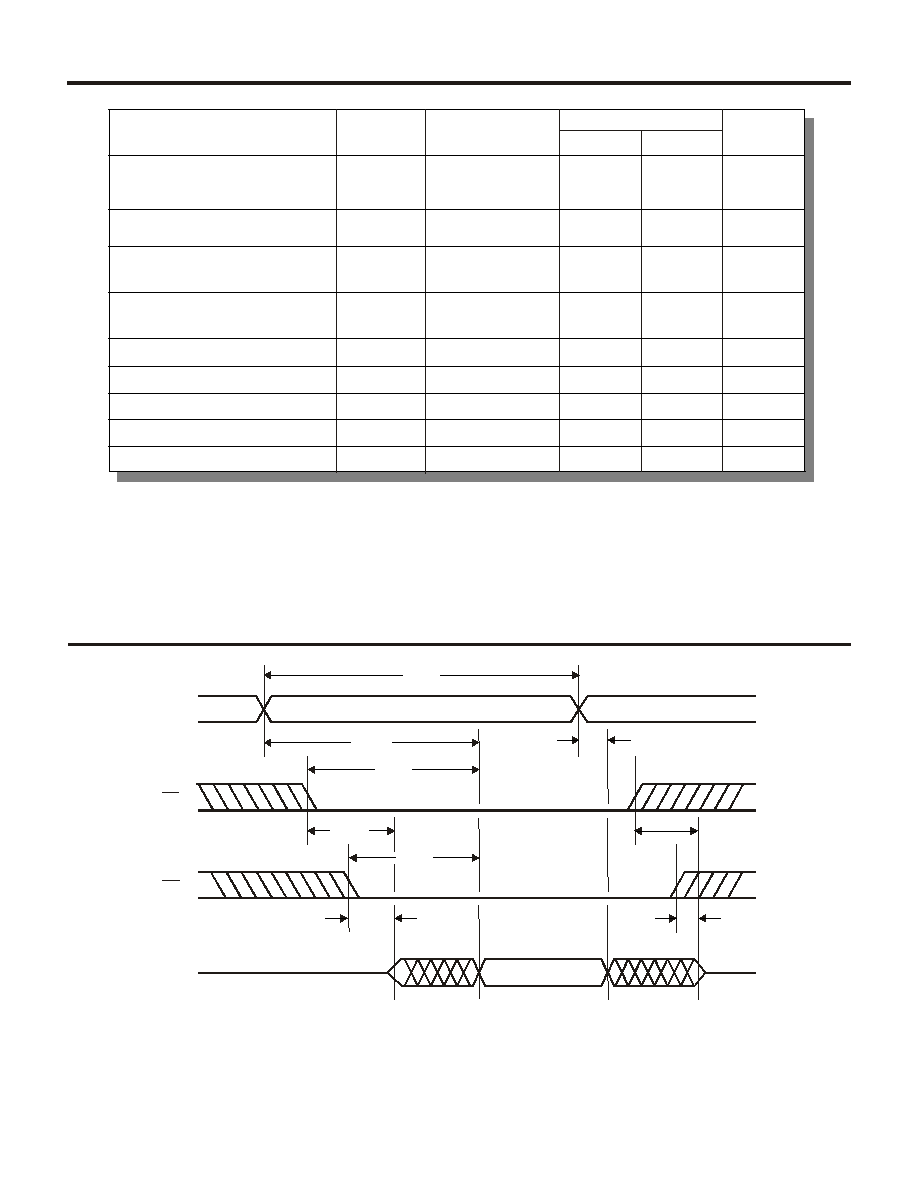
Read Cycle AC Timing Characteristics
(1)
Read Cycle Timing Diagram
Device Type
Limits
Minimum
Maximum
Units
0
0
0
15
15
ns
ns
ns
ns
ns
ns
ns
ns
ns
Test
Read Cycle Time
Address Access Time
Chip Enable Access Time
Output Enable Access Time
Chip Enable to Output Active
Output Enable to Output Active
Output Hold After Address Change
Chip Enable to Output Disable
Output Enable to Output Disable
Symbol
t
EHQZ
t
AVAV
t
AVQV
t
GHQZ
t
GLQV
t
ELQV
t
ELQX
t
GLQX
t
AXQX
t
AVAV
Valid Address
Valid Data
High Impedance
Address
t
AVQV
t
ELQV
t
ELQX
t
GLQV
t
GLQX
CE
OE
Data
Out
t
GHQZ
t
EHQZ
t
AXQX
100
ALL
ALL
100
ALL
100
ALL
100