
BRIGHT Preliminary BM29F400T/BM29F400B
Microelectronics
Inc.
4MEGABIT (512K x 8/ 256K x 16)
5VOLT SECTOR ERASE CMOS FLASH MEMORY
A Winbond Company
Publication Release Date: May 1999
- 1 -
Revision A1
GENERAL DESCRIPTION
The BM29F400 is an 4 Megabit, 5.0 volt-only CMOS Flash memory device organized as a 512
Kbytes of 8-bits each, or 256 Kbytes of 16 bits each. The device is offered in standard 44-pin SOP
and 48-pin TSOP packages. It is designed to be programmed and erased in-system with a 5.0 volt
power-supply and can also be reprogrammed in standard EPROM programmers.
With access times of 90 nS, 120 nS, and 150 nS, the BM29F400 has separate chip enable
CE
, write
enable
WE
, and output enable
OE
controls. BMI's memory devices reliably store memory data even
after 100,000 program and erase cycles.
The BM29F400 is entirely pin and command set compatible with the JEDEC standard for 4 Megabit
Flash memory devices. Commands are written to the command register using standard
microprocessor write timings. Register contents serve as input to an internal state-machine which
controls the erase and programming circuitry. Write cycles also internally latch addresses and data
needed for the programming and erase operations.
The BM29F400 is programmed by executing the program command sequence. This will start the
internal byte/word programming algorithm that automatically times the program pulse width and also
verifies the proper cell margin. Erase is accomplished by executing either the sector erase or chip
erase command sequence. This will start the internal erasing algorithm that automatically times the
erase pulse width and also verifies the proper cell margin. No preprogramming is required prior to
execution of the internal erase algorithm. Sectors of the BM29F400 Flash memory array are
electrically erased via Fowler-Nordheim tunneling. Bytes/words are programmed one byte/word at a
time using a hot electron injection mechanism.
The BM29F400 features a sector erase architecture. The device memory array is divided into one 16
Kbytes, two 8 Kbytes, one 32 Kbytes, and seven 64 Kbytes. Sectors can be erased individually or in
groups without affecting the data in other sectors. Multiple sector erase and full chip erase capabilities
add flexibility to altering the data in the device. To protect this data from accidental program and
erase, the device also has a sector protect function. This function hardware write protects the
selected sector(s). The sector protect and sector unprotect features can be enabled in a PROM
programmer.
For read, program and erase operation, the BM29F400 needs a single 5.0 volt power-supply.
Internally generated and well regulated voltages are provided for the program and erase operation. A
low Vcc detector inhibits write operations on loss of power. End of program or erase is detected by the
Ready/Busy status pin, Data Polling of DQ7, or by the Toggle Bit I feature on DQ6. Once the program
or erase cycle has been successfully completed, the device internally resets to the Read mode.
The BM29F400 also has a hardware
RESET
pin. Driving the
RESET
pin low during execution of an
Internal Programming or Erase command will terminate the operation and reset the device to the
Read mode. The
RESET
pin may be tied to the system reset circuitry, so that the system will have
access to boot code upon completion of system reset, even if the Flash device is in the process of an
Internal Programming or Erase operation. If the device is reset using the
RESET
pin during an
Internal Programming or Erase operation, data in the address locations on which the internal state
BRIGHT Preliminary BM29F400T/BM29F400B
Microelectronics
Inc.
- 2 -
machine is operating will be erroneous. Thus, these address locations will need rewriting after the
device is reset.
FEATURES
�
5.0 V +/- 10% Program and Erase
-
Minimizes system-level power requirements
High performance
-
90 nS access time
�
Compatible with JEDEC-standard Commands
-
Uses software commands, pinouts, and
packages following industry standards for
single power supply Flash memory
�
Typically 100,000 Program/Erase Cycles
�
Sector Erase Architecture
-
One 16 Kbytes, two 8 Kbytes, one 32 Kbytes,
and seven 64 Kbytes
-
Any combination of sectors can be erased
concurrently; also supports full chip erase
�
Erase Suspend/Resume
-
Suspend a sector erase operation to allow a
data read in a sector not being erased within
the same device
�
Ready/Busy
-
RY/BY output pin for detection of
programming or erase cycle completion
�
RESET
-
Hardware pin resets the internal state
machine to the read mode
�
Internal Erase Algorithms
-
Automatically erases a sector, any
combination of sectors, or the entire
chip
�
Internal Programming Algorithms
-
Automatically programs and verifies data at a
specified address
�
Low Power Consumption
-
20 mA typical active read current for Byte
Mode
-
28 mA typical active read current for Word
Mode
-
30 mA typical write/erase current
�
Sector Protection
-
Hardware method disables any combination
of sectors from a program or erase operation
�
Boot Code Sector Architecture
FAMILY PART NO.
-90
-120
-150
Maximum Access Time (nS)
90
120
150
CE
(E) Access time (nS)
90
120
150
OE
(G) Access time (nS)
35
50
60
*This speed is available with Vcc = 5V +/- 5% variation
BRIGHT Preliminary BM29F400T/BM29F400B
Microelectronics
Inc.
A Winbond Company
Publication Release Date: May 1999
- 3 -
Revision A1
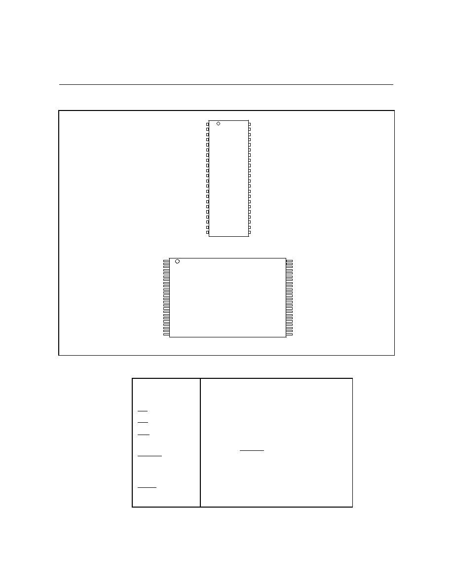
PIN CONFIGURATIONS
1
2
3
4
5
6
7
8
9
10
11
12
13
14
15
16
17
18
19
20
21
22
44
43
42
41
40
39
38
37
36
35
34
33
32
31
30
29
28
27
26
25
24
23
NC
RY/BY
A17
A7
A6
A5
A4
A3
A2
A1
A0
/CE
Vss
/OE
DQ0
DQ8
DQ1
DQ9
DQ2
DQ10
DQ3
DQ11
/RESET
/WE
A8
A9
A10
A11
A12
A13
A14
A15
A16
/BYTE
Vss
DQ15/A-1
DQ7
DQ14
DQ6
DQ13
DQ5
DQ12
DQ4
Vcc
PSOP
A15
A14
A13
A12
A11
A10
A9
A8
NC
NC
/WE
/RESET
NC
NC
RY/BY
NC
A17
A7
A6
A5
A4
A3
A2
A1
48
47
46
45
44
43
42
41
40
39
38
37
36
35
34
33
32
31
30
29
28
27
26
25
1
2
3
4
5
6
7
8
9
10
11
12
13
14
15
16
17
18
19
20
21
22
23
24
A16
/BYTE
Vss
DQ15/A-1
DQ7
DQ14
DQ6
DQ13
DQ5
DQ12
DQ4
Vcc
DQ11
DQ3
DQ10
DQ2
DQ9
DQ1
DQ8
DQ0
/OE
Vss
/CE
A0
Standard TSOP
PIN DESCRIPTION
A0 - A17
DQ0 - DQ14
DQ15 /A-1
CE
OE
WE
Vss
RESET
RY/BY
Vcc
BYTE
NC
Address Inputs
Data Input/Output
Data Input/Output, Address Mux.
Chip Enable
Output Enable
Write Enable
Device Ground
Hardware
RESET
Pin, Active Low
Ready/Busy Status Output
Device Power Supply
Selects 8-bit or 16-bit Mode
Not Internally Connected
BRIGHT Preliminary BM29F400T/BM29F400B
Microelectronics
Inc.
- 4 -
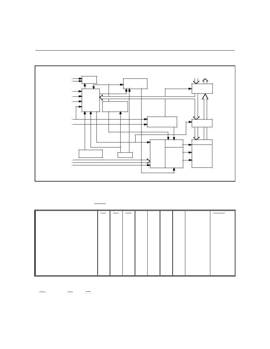
BLOCK DIAGRAM
Vcc
Vss
RY/BY
Buffer
State
Control
Command
Register
Vcc Detector
Timer
PGM Voltage
Generator
Erase Boltage
Generator
Chip Enable
Output Enable
Logic
Input/Output
Buffers
Data Latch
Y-Gating
Cell Matrix
X-Decoder
Y-Decodor
Address
Latch
STB
STB
A0-A16
A-1
/OE
/CE
/WE
/BYTE
/RESET
DQ0-DQ15
BUS OPERATION
Table 1. Bus Operations (
BYTE
= V
IH
)
(1)
OPERATION
CE
OE
WE
A0
A1
A6
A9
DQ0-DQ15
RESET
Electronic ID Manufacturer(2)
L
L
H
L
L
L
V
ID
Code
H
Electronic ID Device(2)
L
L
H
H
L
L
V
ID
Code
H
Read(3)
L
L
H
A0
A1
A6
A9
D
OUT
H
Standby
H
X
X
X
X
X
X
High Z
H
Hardware Reset
X
X
X
X
X
X
X
High Z
L
Output Disable
L
H
H
X
X
X
X
High Z
X
Write
L
H
L
A0
A1
A6
A9
D
IN
(4)
H
Verify Sector Protect(2)
L
L
H
L
H
L
V
ID
Code
H
Temporary Sector Unprotect
X
X
X
X
X
X
X
X
V
ID
Notes:
1. L = V
IL
, H = V
IH
, X = Don't Care. See DC Characteristics for voltage levels.
2. Manufacturer and device codes may also be accessed via a command register sequence. Refer to Table 6.
3. WE can be V
IL
if CE is V
IL
, OE at V
IH
initiates the write operations.
4. Refer to Table 6 for valid DIN during a write operation.
BRIGHT Preliminary BM29F400T/BM29F400B
Microelectronics
Inc.
A Winbond Company
Publication Release Date: May 1999
- 5 -
Revision A1
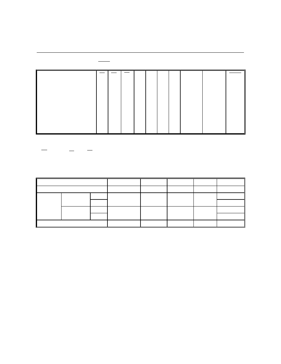
Table 2. Bus Operations (
BYTE
= V
IL
)
(1)
OPERATION
CE
OE
WE
A0
A1
A6
A9
DQ0-DQ7
DQ8-DQ15
RESET
Electronic ID Manufacturer(2)
L
L
H
L
L
L
V
ID
Code
High Z
H
Electronic ID Device(2)
L
L
H
H
L
L
V
ID
Code
High Z
H
Read(3)
L
L
H
A0
A1
A6
A9
D
OUT
High Z
H
Standby
H
X
X
X
X
X
X
High Z
High Z
H
Hardware Reset
X
X
X
X
X
X
X
High Z
High Z
L
Output Disable
L
H
H
X
X
X
X
High Z
High Z
H
Write
L
H
L
A0
A1
A6
A9
D
IN
(4)
High Z
H
Verify Sector Protect(2)
L
L
H
L
H
L
V
ID
Code
High Z
H
Temporary Sector Unprotect
X
X
X
X
X
X
X
X
High Z
V
ID
Notes:
1. L = V
IL
, H = V
IH
, X = Don't Care. See DC Characteristics for voltage levels.
2. Manufacturer and device codes may also be accessed via a command register sequence. Refer to Table 6.
3.
WE
can be V
IL
if CE is V
IL
, OE at V
IH
initiates the write operations.
4. Refer to Table 6 for valid DIN during a write operation.
Table 3. Sector Protection Verify Electronic ID Codes
TYPE
A17-A12
A6
A1
A0
Code (Hex)
Manufacturer Code
X
V
IL
V
IL
V
IL
ADH
29F400T
Byte
X
V
IL
V
IL
V
IH
23H
29F400
Word
22,23H
29F400B
Byte
X
V
IL
V
IL
V
IH
ABH
Word
22 ABH
Sector Protection
Sector Address
V
IL
V
IH
V
IL
01H(1)
Note: Outputs 01H at protected sector addresses, and outputs 00H at unprotected addresses.