Product Specification www.jmnic.com
Silicon NPN Power Transistors
2SC2305
DESCRIPTION
With TO-3PN package
High breakdown voltage
Fast switching speed
Wide safe operating area
APPLICATIONS
For switching regulator applications
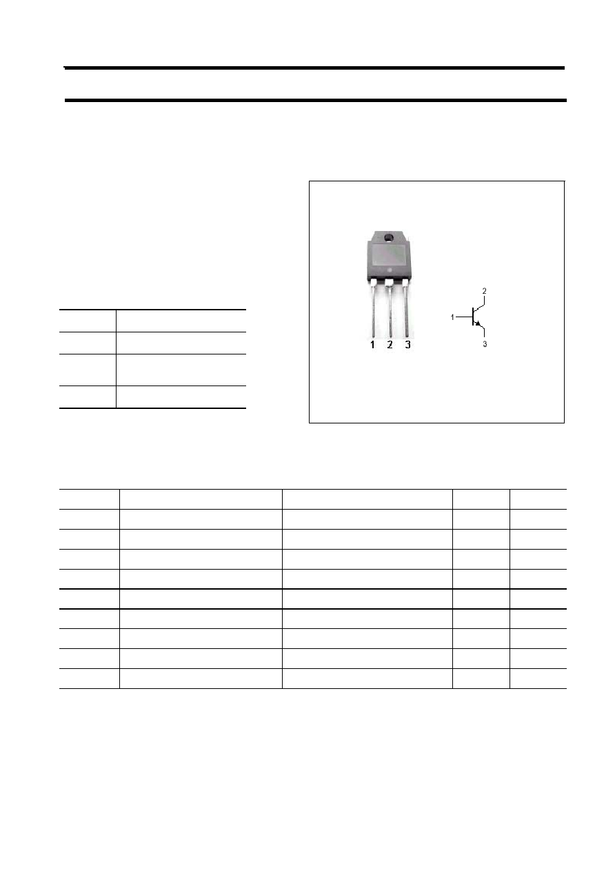
PINNING
PIN DESCRIPTION
1
Base
2
Collector;connected to
mounting base
3 Emitter
Fig.1 simplified outline (TO-3PN) and symbol
Absolute maximum ratings (Ta=25
)
SYMBOL PARAMETER
CONDITIONS VALUE
UNIT
V
CBO
Collector-base voltage
Open emitter
400
V
V
CEO
Collector-emitter voltage
Open base
400
V
V
EBO
Emitter-base voltage
Open collector
8
V
I
C
Collector current (DC)
7
A
I
CP
Collector current (Pulse)
14
A
I
B
Base current (DC)
3
A
P
C
Collector power dissipation
T
C
=25
80
W
T
j
Junction
temperature
150
T
stg
Storage
temperature
-55~150
JM
n
ic

Product Specification www.jmnic.com
JM
n
ic
Silicon NPN Power Transistors
2SC2305
CHARACTERISTICS
Tj=25
unless otherwise specified
SYMBOL PARAMETER
CONDITIONS
MIN
TYP.
MAX
UNIT
V
CEO
Collector-emitter breakdown voltage
I
C
=10mA ;R
BE
=
400
V
V
CBO
Collector-base breakdown voltage
I
C
=1m A; I
E
=0 400
V
V
EBO
Emitter-base breakdown voltage
I
E
=1m A; I
C
=0
7
V
V
CEsat
Collector-emitter saturation voltage
I
C
=4A; I
B
=0.8A
1.0
V
V
BEsat
Base-emitter saturation voltage
I
C
=4A; I
B
=0.8A
1.5
V
I
CBO
Collector cut-off current
V
CB
=400V; I
E
=0
10
A
I
EBO
Emitter cut-off current
V
EB
=5V; I
C
=0
10
A
h
FE-1
DC current gain
I
C
=0.8A ; V
CE
=5V
15 50
h
FE-2
DC current gain
I
C
=4A ; V
CE
=5V 8
Product Specification www.jmnic.com
JM
n
ic
Silicon NPN Power Transistors
2SC2305
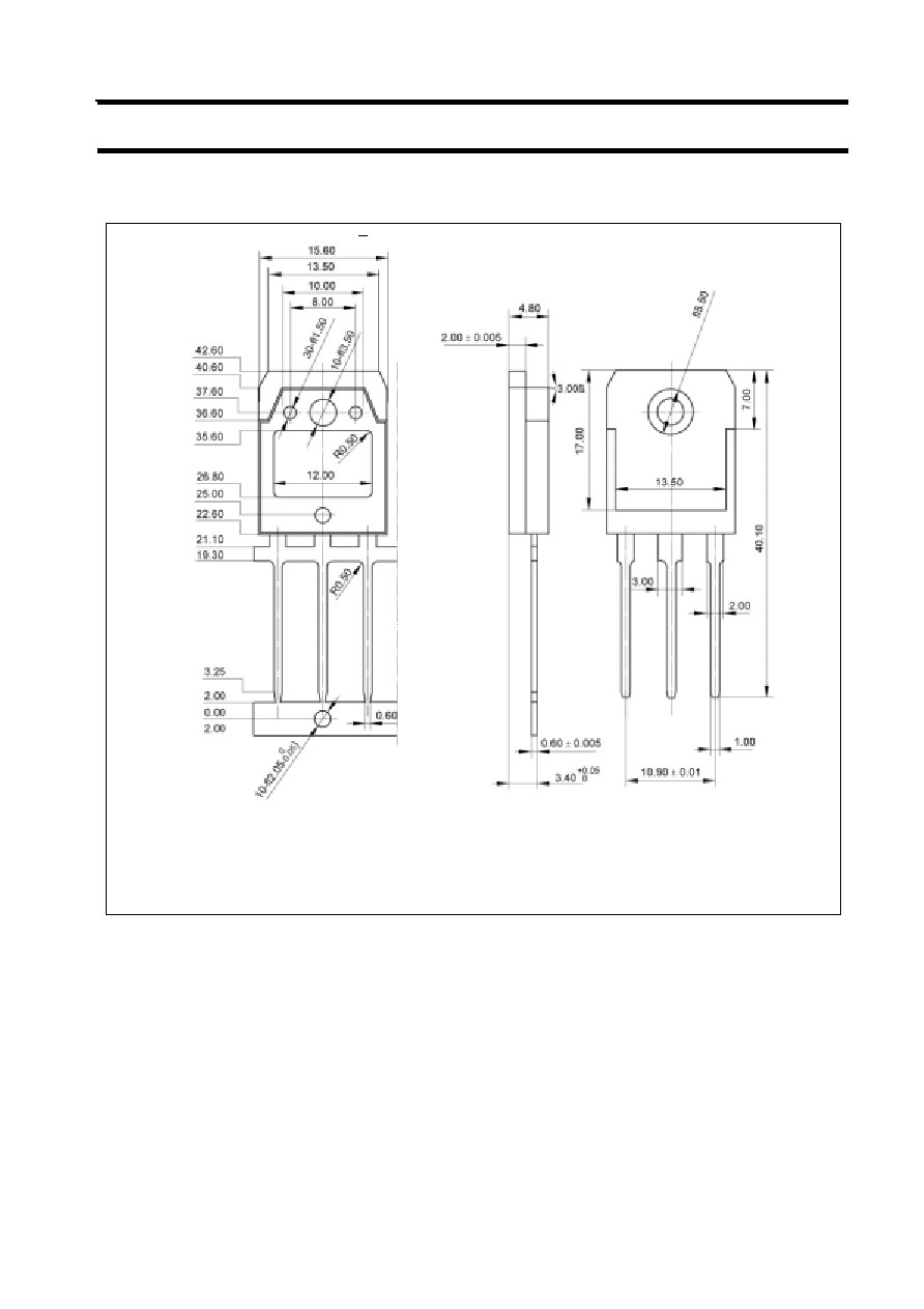
PACKAGE OUTLINE
Fig.2 outline dimensions (unindicated tolerance:
±
0.10 mm)