COMSET SEMICONDUCTORS
1/3
.
BDY53 ≠ BDY54
ABSOLUTE MAXIMUM RATINGS
Symbol
Ratings
Value
Unit
BDY53
60
V
CEO
Collector-Emitter Voltage
BDY54
120
V
BDY53
100
V
CBO
Collector-Base Voltage
BDY54
180
V
V
EBO
Emitter-Base Voltage
BDY53
BDY54
7
V
I
C
Collector Current
BDY53
BDY54
12
A
I
B
Base Current
BDY53
BDY54
5
A
P
TOT
Power Dissipation
@ T
C
= 25∞
BDY53
BDY54
60
Watts
T
J
Junction Temperature
BDY53
BDY54
200
∞C
T
Stg
Storage Temperature
BDY53
BDY54
-65 to +200
∞C
LF Large Signal Power Amplification
High Current Fast Switching
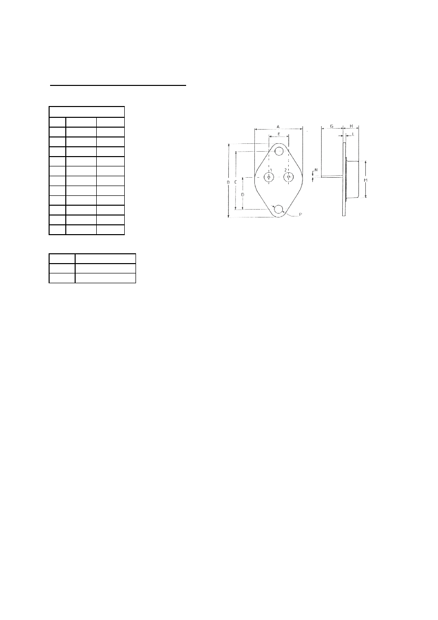
NPN SILICON TRANSISTORS, DIFFUSED MESA
COMSET SEMICONDUCTORS
2/3
BDY53 ≠ BDY54
ELECTRICAL CHARACTERISTICS
TC=25∞C unless otherwise noted
Symbol
Ratings
Test Condition(s)
Min Typ Mx Unit
BDY53
60
-
-
V
CEO(SUS)
Collector-Emitter
Breakdown Voltage (*)
I
C
=100 mA, I
B
=0
BDY54
120
-
-
V
I
EBO
Emitter-Base Cutoff Current
V
EB
=7 V
BDY53
BDY54
-
-
3.0
mA
V
CE
=100 V
V
BE
=-1.5 V
T
CASE
=150∞C
BDY53
-
-
I
CEX
Collector-Emitter Cutoff
Current
V
CE
=150 V
V
BE
=-1.5 V
T
CASE
=150∞C
BDY54
-
-
15
mA
I
C
=4.0 A, I
B
=0.4 A
BDY53
BDY54
-
-
1.1
V
CE(SAT)
Collector-Emitter saturation
Voltage (*)
I
C
=7.0 A, I
B
=1.4 A
BDY53
BDY54
-
-
2.2
V
I
C
=4.0 A, I
B
=0.4 A
BDY53
BDY54
-
-
2
V
BE(SAT)
Base-Emitter Voltage (*)
I
C
=7.0 A, I
B
=1.4 A
BDY53
BDY54
-
-
2.5
V
h
21E
Static Forward Current
transfer ratio (*)
V
CE
=1.5 V, I
C
=2 A
BDY53
BDY54
20
-
60
V
f
T
Transition Frequency
V
CE
=4.0 V, I
C
=0.5 A, f=10
MHz
BDY53
BDY54
20
-
-
MHz
t
d
+ t
r
Turn-on time
I
C
=5 A, I
B
=1 A
BDY53
BDY54
-
0.3
-
µ
s
t
s
+ t
f
Turn-off time
I
C
=5 A,
I
B1
=1 A,
I
B2
=-0.5 A
BDY53
BDY54
-
1.8
-
µ
s
(*) Pulse Width
300
µ
s, Duty Cycle
2.0%