ISOCOM COMPONENTS LTD
Unit 25B, Park View Road West,
Park View Industrial Estate, Brenda Road
Hartlepool, Cleveland, TS25 1YD
Tel: (01429) 863609 Fax :(01429) 863581
ISOCOM INC
720 E., Park Boulevard, Suite 104,
Plano, TX 75074 USA
Tel: (972) 423-5521
Fax: (972) 422-4549
30/7/97
DB91023-AAS/A3
LOW INPUT CURRENT
PHOTODARLINGTON OPTICALLY
COUPLED ISOLATORS
APPROVALS
l
UL recognised, File No. E91231
'X' SPECIFICATION APPROVALS
l
VDE 0884 in 2 available lead form : -
- STD
- G form
VDE 0884 in SMD approval pending
l
EN60950 approved by SETI,
reg. no. 157786-18
4N32X3,-2,-1
4N32-3,-2,-1
DESCRIPTION
The 4N32-3,-2,-1 series of optically coupled
isolators consist of an infrared light emitting
diode and NPN silicon photodarlington in a
space efficient dual in line plastic package.
FEATURES
l
Options :-
10mm lead spread - add G after part no.
Surface mount - add SM after part no.
Tape&reel - add SMT&R after part no.
l
Low input current 0.25mA I
F
l
High CurrentTransfer Ratio (200% min)
l
High Isolation Voltage (5.3kV
RMS
,7.5kV
PK
)
l
High BV
CEO
(55V min)
l
All electrical parameters 100% tested
l
Custom electrical selections available
APPLICATIONS
l
Computer terminals
l
Industrial systems controllers
l
Measuring instruments
l
Signal transmission between systems of
different potentials and impedances
ABSOLUTE MAXIMUM RATINGS
(25∞C unless otherwise specified)
Storage Temperature
-55∞C to + 150∞C
Operating Temperature
-55∞C to + 100∞C
Lead Soldering Temperature
(1/16 inch (1.6mm) from case for 10 secs) 260∞C
INPUT DIODE
Forward Current
80mA
Reverse Voltage
10V
Power Dissipation
105mW
OUTPUT TRANSISTOR
Collector-emitter Voltage BV
CEO
55V
Emitter-collector Voltage BV
ECO
6V
Power Dissipation
150mW
POWER DISSIPATION
Total Power Dissipation
250mW
(derate linearly 3.3mW/∞C above 25∞C)
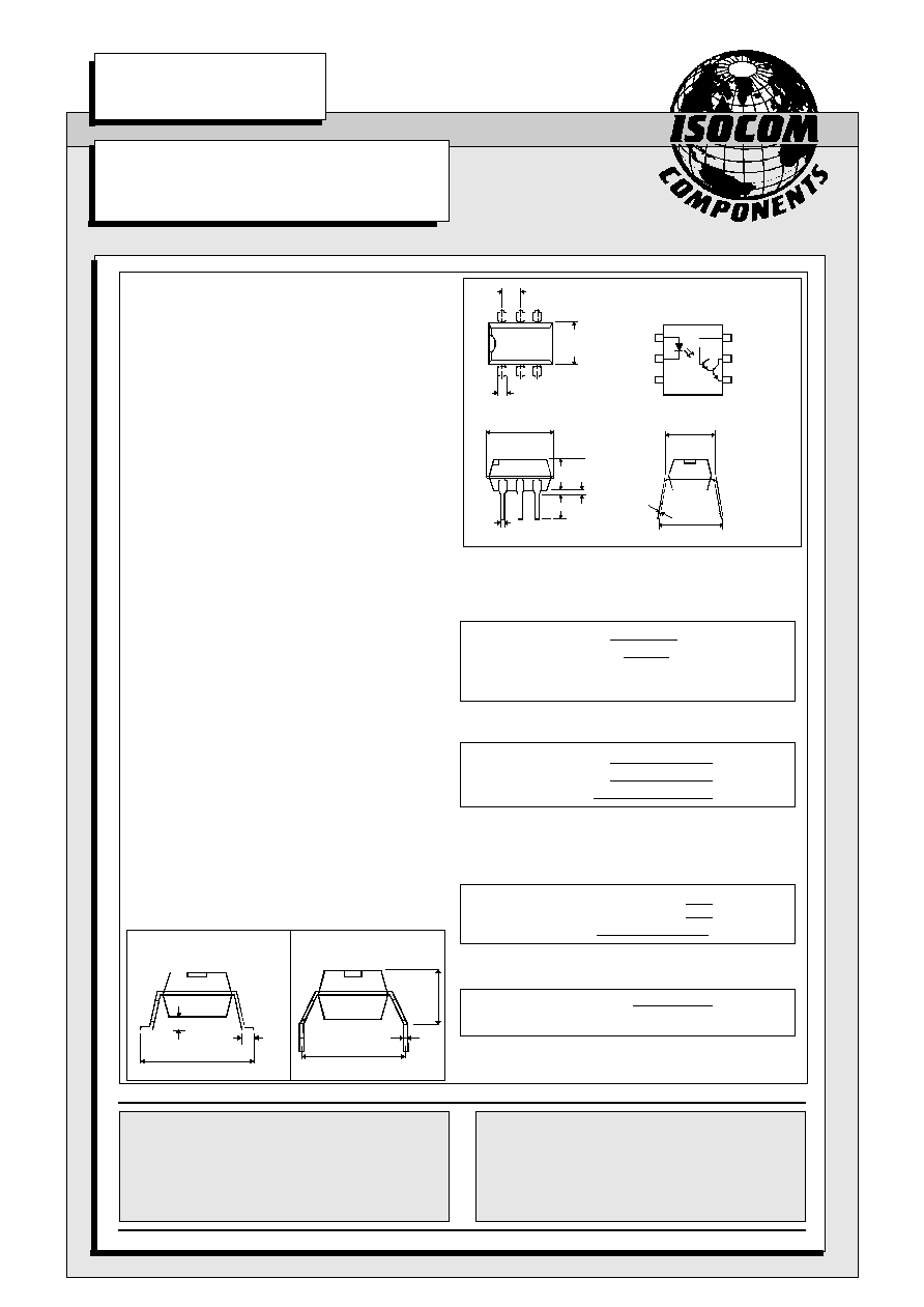
1
3
2
4
6
5
Dimensions in mm
3.3
2.54
6.4
6.2
1.54
8.8
8.4
4.3
4.1
0.5
0.5
0.3
7.8
7.4
9.6
8.4
10.16
0.26
OPTION G
5.08
max.
SURFACE MOUNT
OPTION SM
1.2
0.6
1.4
0.9
10.2
9.5
PARAMETER
MIN TYP MAX UNITS TEST CONDITION
Input
Forward Voltage (V
F
)
1.2
1.4
V
I
F
= 20mA
Reverse Voltage (V
R
)
10
V
I
R
= 10
µ
A
Reverse Current (I
R
)
10
µ
A
V
R
= 10V
Output
Collector-emitter Breakdown (BV
CEO
)
55
V
I
C
= 1mA (note 2)
Collector-base Breakdown (BV
CBO
)
55
V
I
C
= 100
µ
A
Emitter-collector Breakdown (BV
ECO
)
6
V
I
E
= 100
µ
A
Collector-emitter Dark Current (I
CEO
)
100
nA
V
CE
= 10V
Coupled
Current Transfer Ratio (CTR) (Note 2
)
4N32-3
200
%
0.25mA I
F
, 1.0V V
CE
400
%
0.5mA I
F
, 1.0V V
CE
800
%
1.0mA I
F
, 1.0V V
CE
.
4N32-2
400
%
0.5mA I
F
, 1.0V V
CE
800
%
1.0mA I
F
, 1.0V V
CE
.
4N32-1
800
%
1.0mA I
F
, 1.0V V
CE
.
Collector-emitter Saturation Voltage -3
1.0
V
0.25mA I
F
, 0.5mA I
C
-2
1.0
V
0.5mA I
F
, 2mA I
C
-1
1.0
V
1.0mA I
F
, 8mA I
C
Input to Output Isolation Voltage V
ISO
5300
V
RMS
(note 1)
7500
V
PK
(note 1)
Input-output Isolation Resistance R
ISO
5x10
10
V
IO
= 500V (note 1)
Output Rise Time
tr
60
300
µ
s
V
CE
= 2V ,
Output Fall Time
tf
53
250
µ
s
I
C
= 10mA, R
L
= 100
ELECTRICAL CHARACTERISTICS ( T
A
= 25∞C Unless otherwise noted )
Note 1
Measured with input leads shorted together and output leads shorted together.
Note 2
Special Selections are available on request. Please consult the factory.
DB91023-AAS/A3
30/7/97
DB91023-AAS/A3
30/7/97
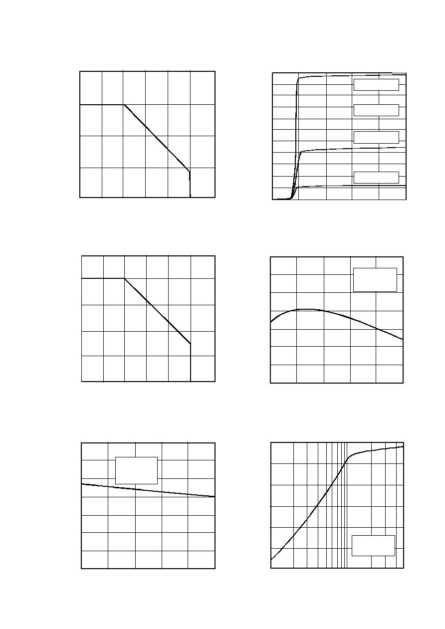
-30 0 25 50 75 100
Ambient temperature T
A
( ∞C )
Collector-emitter saturation voltage V
CE(SA
T
)
(V)
Collector-emitter Saturation
Voltage vs. Ambient Temperature
0
6
10
0
0.2
0.4
0.6
0.8
1.0
1.2
Collector Current vs.
Collector-emitter Voltage
0
0.5
1.0
1.5
0 1 2 3 4 5
4
2
8
Collector-emitter voltage V
CE
( V )
Relative Current Transfer Ratio
vs. Ambient Temperature
I
F
= 1mA
V
CE
= 1V
-30 0 25 50 75 100
Ambient temperature T
A
( ∞C )
Current Transfer Ratio vs. Forward Current
Forward current I
F
(mA)
Current transfer ratio CTR (%)
0
400
600
800
1000
0.1 0.2 0.5 1 2 5
1200
200
V
CE
= 1V
T
A
= 25 ∞C
T
A
= 25∞C
I
F
= 1.0mA
I
F
= 0.25mA
I
F
= 1mA
I
C
= 8mA
I
F
= 0.5mA
50
-30 0 25 50 75 100 125
Ambient temperature T
A
( ∞C )
150
0
200
Ambient temperature T
A
( ∞C )
Collector power dissipation P
C
(mW)
60
20
0
40
-30 0 25 50 75 100 125
Collector Power Dissipation vs. Ambient Temperature
Forward Current vs. Ambient Temperature
100
Forward current I
F
(mA)
80
100
Relative current transfer ratio
Collector current I
C
(mA)