RTI-1
F
EATURES
À
Complete MIL-STD-1553B Remote Terminal
interface compliance
À
Dual-redundant data bus operation supported
À
Internal illegalization of selected mode code
commands
À
External illegal command definition capability
À
Automatic DMA control and address generation
À
Operational status available via dedicated lines or
internal status register
À
ASD/ENASC (formerly SEAFAC) tested and
approved
À
Available in ceramic 84-lead leadless chip carrier and
84-pin pingrid array
À
Full military operating temperature range, -55
∞
C to
+125
∞
C, screened to the specific test methods listed in
Table I of MIL-STD-883, Method 5004, Class B
À
JAN-qualified devices available
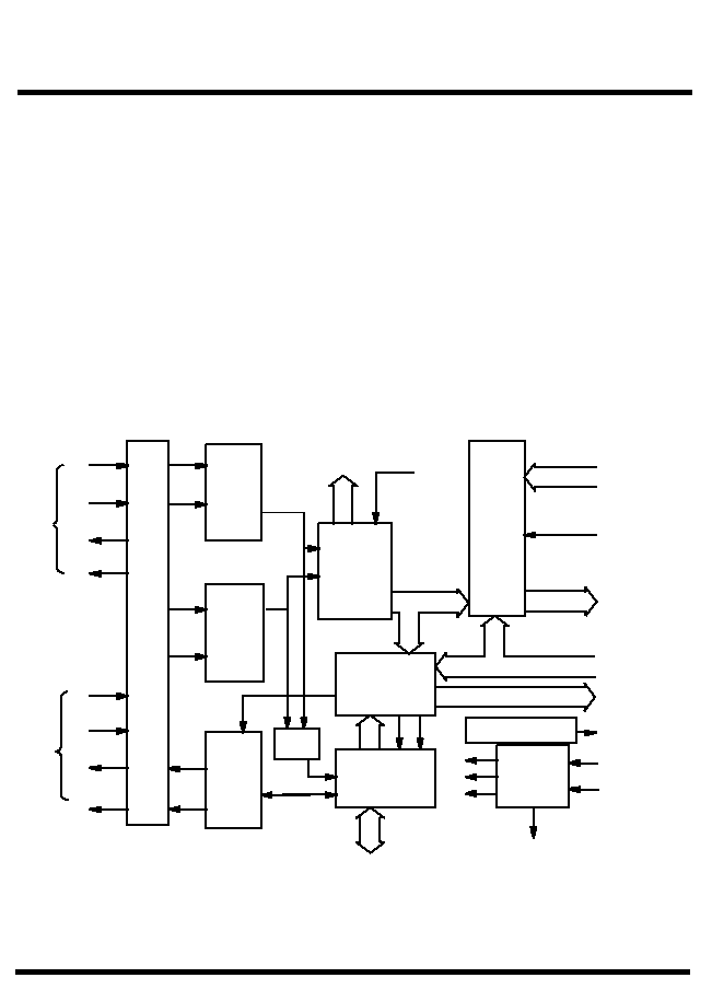
Figure 1. UT1553B RTI Functional Block Diagram
MIL-STD-1553B SERIAL BUS
TRANSCEIVER
I/O
IN
A
OUT
IN
B
OUT
OUTPUT MUL
TIPLEXING AND
SELF TEST
WRAP-AR
OUND
LOGIC
DECODER
CHANNEL
A
DECODER
CHANNEL
B
ENCODER
MUX
16
MODE CODE/
SUB ADDRESS
COMMAND
RECOGNITION
LOGIC
CONTROL
AND
ERROR LOGIC
DATA
TRANSFER
LOGIC
ILLEGAL
COMMAND
MEMORY
ADDRESS
CONTROL
TIMEOUT
CLOCK AND
RESET LOGIC
2MHz
DATA I/O BUS
OUTPUT EN
MEMORY
ADDRESS
OUTPUTS
CONTROL
INPUTS
HOST
SYSTEM
ADDRESS
INPUTS
CONTROL
OUTPUTS
TIMERON
12MHz
RESET
UT1553B RTI Remote Terminal Interface

RTI-2
Table of Contents
1.0 ARCHITECTURE
AND
OPERATION
. . . . . . . . . . . . . . . . . . . . . . . . . . . . . . . . . . .3
1.1
Host Interface . . . . . . . . . . . . . . . . . . . . . . . . . . . . . . . . . . . . . . . . . . . . . . . . . . .3
1.1.1 Direct Memory Access . . . . . . . . . . . . . . . . . . . . . . . . . . . . . . . . . . . . . .3
1.1.2 Transparent Memory Access . . . . . . . . . . . . . . . . . . . . . . . . . . . . . . . . . .4
1.2
Internal Register Description . . . . . . . . . . . . . . . . . . . . . . . . . . . . . . . . . . . . . . .4
1.3
Mode Codes and Subaddresses . . . . . . . . . . . . . . . . . . . . . . . . . . . . . . . . . . . . .7
1.4
MIL-STD-1553B Subaddress and Mode Codes . . . . . . . . . . . . . . . . . . . . . . . .9
1.5
Remote Terminal Address . . . . . . . . . . . . . . . . . . . . . . . . . . . . . . . . . . . . . . . . .9
1.6
Internal Self-Test . . . . . . . . . . . . . . . . . . . . . . . . . . . . . . . . . . . . . . . . . . . . . . .10
1.7
Power-up and Master Reset . . . . . . . . . . . . . . . . . . . . . . . . . . . . . . . . . . . . . . .10
1.8
Encoder and Decoder . . . . . . . . . . . . . . . . . . . . . . . . . . . . . . . . . . . . . . . . . . . .11
1.9
Illegal Command Decoding . . . . . . . . . . . . . . . . . . . . . . . . . . . . . . . . . . . . . . .11
2.0
MEMORY MAP EXAMPLE
. . . . . . . . . . . . . . . . . . . . . . . . . . . . . . . . . . . . . . . . . . . . . . . . . . 12
3.0
PIN IDENTIFICATION AND DESCRIPTION
. . . . . . . . . . . . . . . . . . . . . . . . . . . . . . . . . . . 14
4.0
MAXIMUM AND RECOMMENDED OPERATING CONDITIONS
. . . . . . . . . . . . . . . . . 21
5.0
DC ELECTRICAL CHARACTERISTICS
. . . . . . . . . . . . . . . . . . . . . . . . . . . . . . . . . . . . . . 22
6.0
AC ELECTRICAL CHARACTERISTICS
. . . . . . . . . . . . . . . . . . . . . . . . . . . . . . . . . . . . . . . 23
7.0
PACKAGE OUTLINE DRAWINGS
. . . . . . . . . . . . . . . . . . . . . . . . . . . . . . . . . . . . . . . . . . . . 38

RTI-3
1.0 A
RCHITECTURE
A
ND
O
PERATION
The UT1553B RTI is an interface device linking a MIL-
STD-1553 serial data bus and a host microprocessor system.
The RTI's MIL-STD-1553B interface includes encoding/
decoding logic, error detection, command recognition,
memory address control, clock, and reset circuits.
Decoders
The UT1553B RTI contains two separate free-running
decoders to insure that all redundancy requirements of MIL-
STD-1553B are met. Each decoder receives, decodes, and
verifies biphase Manchester II data. Proper frequency and
edge skew are also verified.
Command Recognition Logic
The command recognition logic monitors the output of both
decoders at all times. Recognition of a valid command
causes a reset of present interface activity followed by
execution of the command. This procedure meets the
requirement for superseding valid commands.
Encoder
The encoder receives serial data from the data transfer logic,
converts it to Manchester II form with proper
synchronization and parity, and passes it to the output and
self-test logic.
Data Transfer Logic
The data transfer logic provides double-buffered 16-bit
parallel-to-serial and serial-to-parallel conversion during
reception and transmission of data.
Memory Address Control
The memory address control logic controls the output of the
three-state address lines during memory access. In DMA
system implementations, the memory address control
provides RTI-generated addresses. In a pseudo-dual-port
memory configuration, the memory address control logic
provides either RTI-generated or host system addressing.
Control and Error Logic
The control and error logic performs the following four
major functions:
-
Interface control for proper processing of MIL-
STD-1553B commands
-
Error checking of both MIL-STD-1553B data and
RTI operation
-
Memory control (DMA or pseudo-dual-port) for
proper data transfer
-
Operational status and control signal generation
Output Multiplexing and Self-Test Logic
This logic directs the output of the encoder to one of four
places:- Channel A outputs
- Channel B outputs
- Channel A decoders during self-test
- Channel B decoders during self-test
Clock and Reset Logic
The UT1553B RTI requires a 12MHz input clock to operate
properly. The RTI provides a 2MHz output for the system
designer to use. The device provides a hardware reset pin
as well as software-generated reset.
Timer Logic
The UT1553B RTI has a built-in 730ms timer that is
activated when the encoder is about to transmit. The timer
is reset upon receipt of a valid command, master reset, or a
time-out condition.
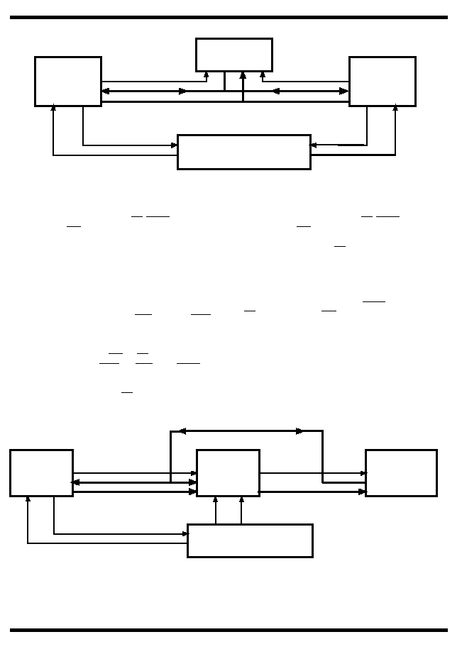
1.1 HOST INTERFACE
Configure the RTI into the host system for either a direct
memory or transparent memory access. The following
sections discuss the system configuration for each method
of memory management.
1.1.1 Direct Memory Access
In the direct memory access configuration the RTI and host
arbitrate for the shared 2K x 16 memory space. To request
access to memory the RTI asserts direct memory request
output (DMARQ); the system bus arbiter grants the RTI
access to memory by asserting the direct memory access
grant signal (MEMCK). The system arbiter should not assert
the MEMCK signal before the RTI has requested access to
memory (i.e., DMARQ asserted).
Once granted access to memory, the RTI address out
(ADDR OUT(10:0)), RAM chip select (RCS), RAM read/
write (RRD/RWR), and Data bus (DATA I/O(15:0)) provide
the interface signals to control the memory access. Figure
2 shows an example of a direct memory access system
configuration; for clarity the interface buffers and logic are
excluded. The host microprocessor also gains access to
memory by arbitration.
Take care to insure that bus contention does not occur
between the host and RTI Address buses or memory control
signals. To place the RTI Address Out bus in a high
impedance state negate the ADOEN input pin. Also note
that outputs RCS and RRD/RWR are not three-state outputs.
When the RTI is not writing to memory, bidirectional Data
bus DATA I/O(15:0) is an input (i.e., not actively driving
the bus).
RTI-4
The host microprocessor gains access to the RTI internal
registers by controlling input pins CS, CTRL, ADDR IN
(10:0), and RD/WR. During message processing the host
microprocessor should limit access to RTI internal registers.
1.1.2 Transparent Memory Access
Configured in the transparent memory mode the host
microprocessor accesses shared memory through the RTI.
Arbitration for access to the bus is performed as discussed
in section 1.1.1 of this document.
When granted access to memory, the RTI asserts memory
control signals ADDR OUT(10:0), RCS, and RRD/RWR.
For host-controlled memory accesses the RAM memory
address from the host is propagated from the Address In bus
ADDR IN (10:0) to the Address Out bus ADDR OUT (10:0).
Memory control signals RD/WR and CS are also propagated
through the RTI as RRD/RWR and RCS. Input CTRL is
negated during all transparent memory accesses to prevent
the RTI from inadvertently performing an internal register
access or software reset. While CS is asserted, the RTI's
bidirectional Data bus DATA I/O (15:0) is an input (i.e., not
actively driving bus).
The host microprocessor gains access to the RTI internal
registers by controlling input pins CS, CTRL, ADDR IN
(10:0), and RD/WR. During message processing the host
microprocessor should limit access to RTI internal registers.
The host should not assert CS while the RTI is performing
a memory access.
1.2 Internal Register Description
The RTI uses three internal registers to allow the host to
control the RTI operation and monitor its status. The host
uses the following inputs Control (CTRL), Chip Select
(CS), Read/Write (RD/WR), and ADDR IN (0) to read the
16-bit System Register or write to the 8-bit Control Register.
The Control Register toggles bits in the MIL-STD-1553B
status word, enables biphase inputs, selects terminal active
flag, and puts the part in self-test. The System Register
supplies operational status of the UT1553B RTI to the host.
The Last Command Register saves the command word for
a Transmit Last Command mode code, along with
operational status from the System Register.
Shared
Memory
Host
Computer
RTI
UT1553B
DMA
CONTROLLER
Figure 2. Direct Memory Access Configuration
DATA(15:0)
ADDR(10:0)
CONTROL
CONTROL
Control Register (Write Only)
Figure 3. Transparent Memory Access Configuration
Shared
Memory
Host
Computer
RTI
UT1553B
DMA
CONTROLLER
DATA(15:0)
ADDR IN (10:0)
CONTROL
ADDR OUT (10:0)
CONTROL
DATA I/O (15:0)
RTI-5
The 8-bit write-only Control Register manages the operation of the RTI. Write to the Control Register by applying a logic zero
to CS, CTRL, RD/WR, and ADDR IN (0); if ADDR IN (0) is a logic one a master reset occurs. Data is loaded into the Control
Register via I/O pins DATA(7:0). Control Register writes must occur 50ns before the rising edge of COMSTR to latch data in
the outgoing status word.
System Register (Read Only)
The 16-bit read-only System Register provides the RTI system status. Read the System Register by applying a logic zero to
CS, CTRL, ADDR IN (0), and a logic one to RD/WR. The 16-bit contents of the System Register are read from data I/O pins
DATA(15:0).
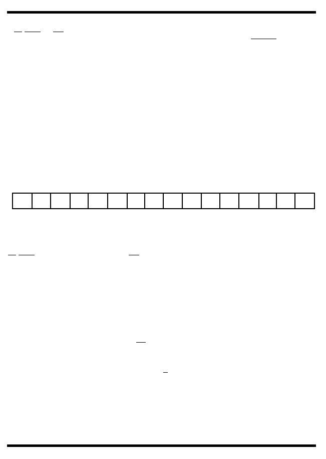
Bit
Number
Initial
Condition Description
0
[0]
Channel A Enable. A logic one enables Channel A biphase inputs.
1
[0]
Channel B Enable. A logic one enables Channel B biphase inputs.
2
[0]
Terminal Flag. A logic one sets the Terminal Flag bit of the Status Register.
3
[0]
System Busy. A logic one sets the Busy bit of the System Register and inhibits
RTI access to memory. No data words are retrieved or stored; command word is
stored.
4
[0]
Subsystem Busy. A logic one sets the Subsystem Flag bit of the Status Register.
5
[0]
Self-Test Channel Select. This bit selects which channel the internal self-test
checks; a logic one selects Channel A and a logic zero selects Channel B.
6
[0]
Self-Test Enable. A logic one sets the RTI in the internal self-test mode and inhib-
its normal operation. Internal testing is not visible on biphase output
channels.
7
[0]
Service Request. A logic one sets the Service Request bit of the Status Register.
X
SRV
RQ
SELF
TEST
SUBS
BUSY
TF
CH B
EN
CH A
EN
SELF
CH
[ ] defines reset state
CONTROL REGISTER (WRITE ONLY)
MSB
Figure 4. Control Register
X
X
X
X
X
X
X
[0]
[0]
[0] [0] [0] [0] [0] [0]
LSB
Bit
Number
Initial
Condition
Description
0
[0]
MCSA(0). The LSB of the mode code or subaddress as indicated by the
logic state of bit 5.
1
[0]
MCSA(1). Mode code or subaddress as indicated by the state of bit 5.
2
[0]
MCSA(2). Mode code or subaddress as indicated by the state of bit 5.
3
[0]
MCSA(3). Mode code or subaddress as indicated by the state of bit 5.
4
[0]
MCSA(4). Mode code or subaddress as indicated by the state of bit 5.
5
[0] MC/SA. A logic one indicates that bits 4 through 0 are the subaddress of
the last command word, and that the last command word was a normal
transmit orreceive command. A logic zero indicates that bits 4 through 0
are a mode code, and that the last command was a mode code.
6 [1]
Channel
A/B. A logic one indicates that the most recent command arrived
onChannel A; a logic zero indicates that it arrived on Channel B.