REVISIONS
LTR
DESCRIPTION
DATE (YR-MO-DA)
APPROVED
D
Add vendor CAGE F8859. Add device class V criteria. Editorial changes
throughout. - jak
99-11-05
Monica L. Poelking
E
Correct data limits in paragraph 1.3 and I
IN
test conditions in table I. Add case
outline X. Add table III, delta limits. Editorial changes throughout. - jak
00-06-21
Monica L. Poelking
F
Correct table II. Update boilerplate to MIL-PRF-38535 requirements. � jak
02-02-08
Thomas M. Hess
CURRENT CAGE CODE 67268
REV
SHEET
REV
F
F
SHEET
15
16
REV STATUS
REV
F
F
F
F
F
F
F
F
F
F
F
F
F
F
OF SHEETS
SHEET
1
2
3
4
5
6
7
8
9
10
11
12
13
14
PMIC N/A
PREPARED BY
Greg A. Pitz
DEFENSE SUPPLY CENTER COLUMBUS
STANDARD
MICROCIRCUIT
DRAWING
CHECKED BY
D. A. DiCenzo
COLUMBUS, OHIO 43216
http://www.dscc.dla.mil
THIS DRAWING IS AVAILABLE
FOR USE BY ALL
DEPARTMENTS
APPROVED BY
Robert P. Evans
MICROCIRCUIT, DIGITAL, HIGH-SPEED CMOS, OCTAL
TRANSPARENT D-TYPE LATCHES WITH THREE-
STATE OUTPUTS, MONOLITHIC SILICON
AND AGENCIES OF THE
DEPARTMENT OF DEFENSE
DRAWING APPROVAL DATE
84-10-17
AMSC N/A
REVISION LEVEL
F
SIZE
A
CAGE CODE
14933
84072
SHEET
1 OF
16
DSCC FORM 2233
APR 97
5962-E206-02
DISTRIBUTION STATEMENT A. Approved for public release; distribution is unlimited.
STANDARD
MICROCIRCUIT DRAWING
SIZE
A
84072
DEFENSE SUPPLY CENTER COLUMBUS
COLUMBUS, OHIO 43216-5000
REVISION LEVEL
F
SHEET
2
DSCC FORM 2234
APR 97
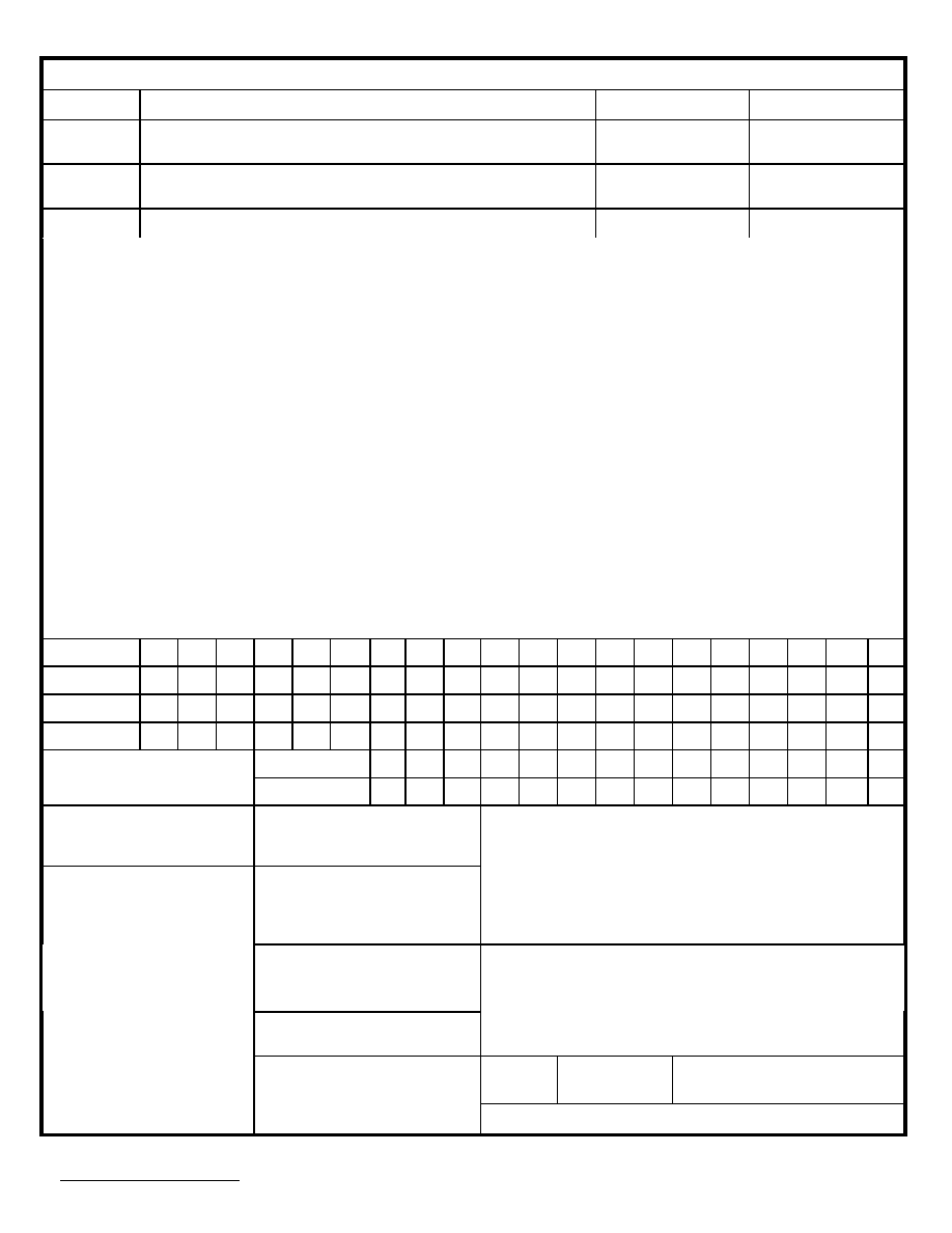
1. SCOPE
1.1 Scope. This drawing documents two product assurance class levels consisting of high reliability (device classes Q and M)
and space application (device class V). A choice of case outlines and lead finishes are available and are reflected in the Part or
Identifying Number (PIN). When available, a choice of Radiation Hardness Assurance (RHA) levels are reflected in the PIN.
1.2 PIN. The PIN is as shown in the following examples.
84072
01 R X
Drawing number Device type Case outline Lead finish
(see 1.2.2) (see 1.2.4) (see 1.2.5)
For device class V:
5962 - 84072
01
V
X
X
Federal
RHA
Device
Device
Case
Lead
stock class
designator
type
class
outline
finish
designator
(see 1.2.1)
(see 1.2.2)
designator
(see 1.2.4)
(see 1.2.5)
\ /
(see
1.2.3)
\/
Drawing number
1.2.1 RHA designator. Device classes Q and V RHA marked devices meet the MIL-PRF-38535 specified RHA levels and are
marked with the appropriate RHA designator. Device class M RHA marked devices meet the MIL-PRF-38535, appendix A
specified RHA levels and are marked with the appropriate RHA designator. A dash (-) indicates a non-RHA device.
1.2.2 Device type(s). The device type(s) identify the circuit function as follows:
Device type Generic
number Circuit
function
01
54HC373
Octal transparent D-type latches with
three-state
outputs
1.2.3 Device class designator. The device class designator is a single letter identifying the product assurance level as listed
below. Since the device class designator has been added after the original issuance of this drawing, device classes M and Q
designators will not be included in the PIN and will not be marked on the device.
Device class
Device requirements documentation
M
Vendor self-certification to the requirements for MIL-STD-883 compliant, non-JAN
class level B microcircuits in accordance with MIL-PRF-38535, appendix A
Q or V
Certification and qualification to MIL-PRF-38535
1.2.4 Case outline(s). The case outline(s) are as designated in MIL-STD-1835 and as follows:
Outline letter Descriptive
designator Terminals Package
style
R
GDIP1-T20 or CDIP2-T20
20
Dual-in-line
S
GDFP2-F20 or CDFP3-F20
20
Flat pack
X
See figure 1
20
Flat pack
2
CQCC1-N20
20
Square leadless chip carrier
STANDARD
MICROCIRCUIT DRAWING
SIZE
A
84072
DEFENSE SUPPLY CENTER COLUMBUS
COLUMBUS, OHIO 43216-5000
REVISION LEVEL
F
SHEET
3
DSCC FORM 2234
APR 97
1.2.5 Lead finish. The lead finish is as specified in MIL-PRF-38535 for device classes Q and V or MIL-PRF-38535, appendix A
for device class M.
1.3 Absolute maximum ratings. 1/ 2/ 3/
Supply voltage range (V
CC
).................................................................................. -0.5 V dc to +7.0 V dc
DC input voltage range (V
IN
)................................................................................ -0.5 V dc to V
CC
+0.5 V dc
DC output voltage range (V
OUT
)........................................................................... -0.5 V dc to V
CC
+0.5 V dc
Input clamp current (I
IK
) (V
IN
< 0.0 or V
IN
> V
CC
) ..................................................
�
20 mA
Output clamp current (I
OK
) (V
OUT
< 0.0 or V
OUT
> V
CC
).........................................
�
20 mA
Continuous output current (I
OUT
) (V
OUT
= 0.0 to V
CC
) ...........................................
�
35 mA
Continuous current through V
CC
or GND .............................................................
�
70 mA
Storage temperature range (T
STG
) ....................................................................... -65
�
C to +150
�
C
Maximum power dissipation (P
D
):........................................................................ 500 mW 4/
Lead temperature (soldering, 10 seconds).......................................................... +260
�
C
Thermal resistance, junction-to-case (
JC
) .......................................................... See MIL-STD-1835
Junction temperature (T
J
) .................................................................................... +175
�
C 5/
1.4 Recommended operating conditions. 2/ 3/
Supply voltage range (V
CC
).................................................................................. +2.0 V dc to +6.0 V dc
Case operating temperature range (T
C
) ............................................................. -55
�
C to +125
�
C
Input rise or fall time t
r
, t
f
):
VCC = 2.0 V ...................................................................................................... 0 to 1,000 ns
VCC = 4.5 V ...................................................................................................... 0 to 500 ns
VCC = 6.0 V ...................................................................................................... 0 to 400 ns
Minimum setup time, data before LE
(t
s
):
T
C
= +25
�
C:
V
CC
= 2.0 V ........................................................................................................ 100 ns
V
CC
= 4.5 V ........................................................................................................ 20 ns
V
CC
= 6.0 V ........................................................................................................ 17 ns
T
C
= -55
�
C to +125
�
C:
V
CC
= 2.0 V ........................................................................................................ 150 ns
V
CC
= 4.5 V ........................................................................................................ 30 ns
V
CC
= 6.0 V ........................................................................................................ 26 ns
1/ Stresses above the absolute maximum rating may cause permanent damage to the device. Extended operation at the
maximum levels may degrade performance and affect reliability.
2/ Unless otherwise noted, all voltages are referenced to GND.
3/ The limits for the parameters specified herein shall apply over the full specified V
CC
range and case temperature range of
-55
�
C to +125
�
C.
4/ For T
C
= +100
�
C to +125
�
C, derate linearly at 12 mW/
�
C.
5/ Maximum junction temperature shall not be exceeded except for allowable short duration burn-in screening conditions in
accordance with method 5004 of MIL-STD-883.

STANDARD
MICROCIRCUIT DRAWING
SIZE
A
84072
DEFENSE SUPPLY CENTER COLUMBUS
COLUMBUS, OHIO 43216-5000
REVISION LEVEL
F
SHEET
4
DSCC FORM 2234
APR 97
Minimum hold time, data after LE
(t
h
):
T
C
= +25
�
C:
V
CC
= 2.0 V ........................................................................................................ 50 ns
V
CC
= 4.5 V ........................................................................................................ 10 ns
V
CC
= 6.0 V ........................................................................................................ 10 ns
T
C
= -55
�
C to +125
�
C:
V
CC
= 2.0 V ........................................................................................................ 75 ns
V
CC
= 4.5 V ........................................................................................................ 15 ns
V
CC
= 6.0 V ........................................................................................................ 13 ns
Minimum pulse width LE high (t
w
):
T
C
= +25
�
C:
V
CC
= 2.0 V ........................................................................................................ 100 ns
V
CC
= 4.5 V ........................................................................................................ 20 ns
V
CC
= 6.0 V ........................................................................................................ 17 ns
T
C
= -55
�
C to +125
�
C:
V
CC
= 2.0 V ........................................................................................................ 150 ns
V
CC
= 4.5 V ........................................................................................................ 30 ns
V
CC
= 6.0 V ........................................................................................................ 26 ns
2. APPLICABLE DOCUMENTS
2.1 Government specification, standards, and handbooks. The following specification, standards, and handbooks form a part
of this drawing to the extent specified herein. Unless otherwise specified, the issues of these documents are those listed in the
issue of the Department of Defense Index of Specifications and Standards (DoDISS) and supplement thereto, cited in the
solicitation.
SPECIFICATION
DEPARTMENT
OF
DEFENSE
MIL-PRF-38535 - Integrated Circuits, Manufacturing, General Specification for.
STANDARDS
DEPARTMENT
OF
DEFENSE
MIL-STD-883 - Test
Method
Standard
Microcircuits.
MIL-STD-1835 - Interface
Standard
Electronic Component Case Outlines.
HANDBOOKS
DEPARTMENT
OF
DEFENSE
MIL-HDBK-103 - List of Standard Microcircuit Drawings.
MIL-HDBK-780 - Standard
Microcircuit
Drawings.
(Unless otherwise indicated, copies of the specification, standards, and handbooks are available from the Standardization
Document Order Desk, 700 Robbins Avenue, Building 4D, Philadelphia, PA 19111-5094.)
2.2 Order of precedence. In the event of a conflict between the text of this drawing and the references cited herein, the text of
this drawing takes precedence. Nothing in this document, however, supersedes applicable laws and regulations unless a specific
exemption has been obtained.
STANDARD
MICROCIRCUIT DRAWING
SIZE
A
84072
DEFENSE SUPPLY CENTER COLUMBUS
COLUMBUS, OHIO 43216-5000
REVISION LEVEL
F
SHEET
5
DSCC FORM 2234
APR 97
3. REQUIREMENTS
3.1 Item requirements. The individual item requirements for device classes Q and V shall be in accordance with
MIL-PRF-38535 and as specified herein or as modified in the device manufacturer's Quality Management (QM) plan. The
modification in the QM plan shall not affect the form, fit, or function as described herein. The individual item requirements for
device class M shall be in accordance with MIL-PRF-38535, appendix A for non-JAN class level B devices and as specified
herein.
3.2 Design, construction, and physical dimensions. The design, construction, and physical dimensions shall be as specified in
MIL-PRF-38535 and herein for device classes Q and V or MIL-PRF-38535, appendix A and herein for device class M.
3.2.1 Case outlines. The case outlines shall be in accordance with 1.2.4 herein and figure 1.
3.2.2 Terminal
connections. The terminal connections shall be as specified on figure 2.
3.2.3 Truth
table. The truth table shall be as specified on figure 3.
3.2.4 Logic
diagram. The logic diagram shall be as specified on figure 4.
3.2.5 Switching waveforms and test circuit. The switching waveforms and test circuit shall be as specified in figure 5.
3.3 Electrical performance characteristics and postirradiation parameter limits. Unless otherwise specified herein, the
electrical performance characteristics and postirradiation parameter limits are as specified in table I and shall apply over the full
case operating temperature range.
3.4 Electrical test requirements. The electrical test requirements shall be the subgroups specified in table II. The electrical
tests for each subgroup are defined in table I.
3.5 Marking. The part shall be marked with the PIN listed in 1.2 herein. In addition, the manufacturer's PIN may also be
marked as listed in MIL-HDBK-103. For packages where marking of the entire SMD PIN number is not feasible due to space
limitations, the manufacturer has the option of not marking the "5962-" on the device. For RHA product using this option, the
RHA designator shall still be marked. Marking for device classes Q and V shall be in accordance with MIL-PRF-38535. Marking
for device class M shall be in accordance with MIL-PRF-38535, appendix A.
3.5.1 Certification/compliance mark. The certification mark for device classes Q and V shall be a "QML" or "Q" as required in
MIL-PRF-38535. The compliance mark for device class M shall be a "C" as required in MIL-PRF-38535, appendix A.
3.6 Certificate of compliance. For device classes Q and V, a certificate of compliance shall be required from a QML-38535
listed manufacturer in order to supply to the requirements of this drawing (see 6.6.1 herein). For device class M, a certificate of
compliance shall be required from a manufacturer in order to be listed as an approved source of supply in MIL-HDBK-103 (see
6.6.2 herein). The certificate of compliance submitted to DSCC-VA prior to listing as an approved source of supply for this
drawing shall affirm that the manufacturer's product meets, for device classes Q and V, the requirements of MIL-PRF-38535 and
herein or for device class M, the requirements of MIL-PRF-38535, appendix A and herein.
3.7 Certificate of conformance. A certificate of conformance as required for device classes Q and V in MIL-PRF-38535 or
for device class M in MIL-PRF-38535, appendix A shall be provided with each lot of microcircuits delivered to this drawing.
3.8 Notification of change for device class M. For device class M, notification to DSCC-VA of change of product (see 6.2
herein) involving devices acquired to this drawing is required for any change as defined in MIL-PRF-38535, appendix A.
3.9 Verification and review for device class M. For device class M, DSCC, DSCC's agent, and the acquiring activity retain the
option to review the manufacturer's facility and applicable required documentation. Offshore documentation shall be made
available onshore at the option of the reviewer.
3.10 Microcircuit group assignment for device class M. Device class M devices covered by this drawing shall be in microcircuit
group number 36 (see MIL-PRF-38535, appendix A).