 | –≠–ª–µ–∫—Ç—Ä–æ–Ω–Ω—ã–π –∫–æ–º–ø–æ–Ω–µ–Ω—Ç: 854H8Y2-5 | –°–∫–∞—á–∞—Ç—å:  PDF PDF  ZIP ZIP |
25 Locust St, Haverhill, Massachusetts 01830 ∑ Tel: 800/252-7074, 978/374-0761 ∑ FAX: 978/521-1839
e-mail: sales@freqdev.com ∑ Web Address: http://www.freqdev.com
0.1 Hz to 102.4 kHz
8-Bit Programmable
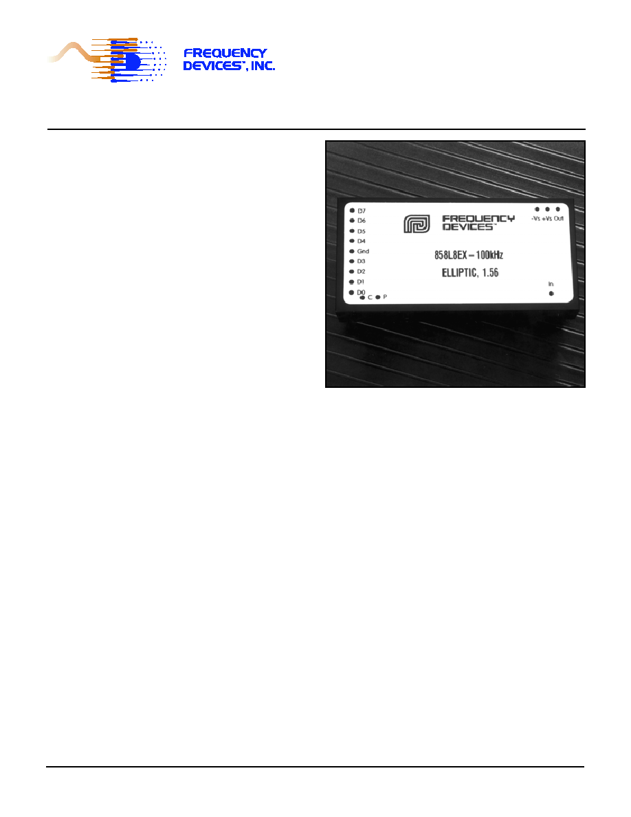
854 Series
2" x 4"
4-Pole Filters
Description
The 854 Series are digitally programmable low-pass
and high-pass active filters that are tunable over a
256:1 frequency range. 854 filters are available with
any one of six standard factory-set tuning ranges up
to 102.4 kHz. These units contain 8 CMOS logic
inputs that can be operated in a transparent or
latching mode.
All 854 Series models are convenient, low profile,
easy to use fully finished filters which require no
external components or adjustments. They feature
low harmonic distortion, and near theoretical phase
and amplitude characteristics. 854 filters operate
from non-critical ±12 to ±18 Vdc power supplies,
have a 10 k (min.) input impedance, a 10 (max.)
output impedance and offer dc voltage offset
adjustment.
Features/Benefits:
∑ Digitally programmable corner frequency allows
selecting cut-off frequencies specific to each
application.
∑ Plug-in ready-to-use, reducing engineering design
and manufacturing cycle time.
∑ Factory-set tuning range, no external clocks or
adjustments needed.
∑ Broad range of transfer characteristics and corner
frequencies to meet a wide range of applications.
∑ Low profile design, ideal for rack mount
installations.
Applications
∑ Anti-alias filtering
∑ Data acquisition systems
∑ Communication systems and electronics
∑ Medical electronics equipment and research
∑ Aerospace, navigation and sonar applications
∑ Sound and vibration testing
∑ Real and compressed time data analysis
∑ Noise elimination
∑ Signal reconstruction
Programmable Specifications
. . . . . . . . . . . . .
Page
Digital Tuning & Control . . . . . . . . . . . . . . . . . . . . . . 2
Available Low-Pass Models:
. . . . . . . . . . . . . . . . . . .
854L4B
4-pole Butterworth . . . . . . . . . . . . . . . . . . 3
854L4L
4-pole Bessel . . . . . . . . . . . . . . . . . . . . . . 3
854L8Y2 4-pole Cheby (0.2 dB Ripple) . . . . . . . . . . 3
854L8Y5 4-pole Cheby (0.5 dB Ripple) . . . . . . . . . . 3
Available High-Pass Models:
. . . . . . . . . . . . . . . . . .
854H8B
4-pole Butterworth . . . . . . . . . . . . . . . . . . 4
854H8Y2 4-pole Cheby (0.2 dB Ripple) . . . . . . . . . . 4
854H8Y5 4-pole Cheby (0.5 dB Ripple) . . . . . . . . . . 4
General Specifications:
Ordering information . . . . . . . . . . . . . . . . . . . . . . . . . 5
Pin-out/package data. . . . . . . . . . . . . . . . . . . . . . . . . 5
8-Bit Programmable Filters
854 Series
Digital Tuning &
Control Characteristics
25 Locust St, Haverhill, Massachusetts 01830 ∑ Tel: 800/252-7074, 978/374-0761 ∑ FAX: 978/521-1839
e-mail: sales@freqdev.com ∑ Web Address: http://www.freqdev.com
2
MSB
---
---
---
---
---
---
LSB
2
7
2
6
2
5
2
4
2
3
2
2
2
1
2
0
D
7
D
6
D
5
D
4
D
3
D
2
D
1
D
0
0
0
0
0
0
0
0
0
f
max
/256
0
0
0
0
0
0
0
1
f
max
/128
0
0
0
0
0
0
1
1
f
max
/64
0
0
0
0
0
1
1
1
f
max
/32
0
0
0
0
1
1
1
1
f
max
/16
0
0
0
1
1
1
1
1
f
max
/8
0
0
1
1
1
1
1
1
f
max
/4
0
1
1
1
1
1
1
1
f
max
/2
1
1
1
1
1
1
1
1
fmax
Bit
Weight
fc
Corner
Frequency
+Vs
OUT
-Vs
D
D
D
D
GND
D
D
D
D
C
P
IN
Bottom View
Os
4
5
3
2
1
0
6
7
Pin-Out Key
IN
Analog Input Signal
D
7
Tuning Bit 7 (MSB)
OUT Analog Output Signal
D
6
Tuning Bit 6
GND Power and Signal Return
D
5
Tuning Bit 5
"P"
Transition Polarity Bit
D
4
Tuning Bit 4
"C"
Tuning Strobe Bit
D
3
Tuning Bit 3
+Vs
Supply Voltage, Positive
D
2
Tuning Bit 2
-Vs
Supply Voltage, Negative
D
1
Tuning Bit 1
Os
Optional Offset Adjustment
D
0
Tuning Bit 0 (LSB)
Digital Tuning Characteristics
The digital tuning interface circuits are two 4042 quad CMOS
latches which accept the following CMOS-compatible inputs:
eight tuning bits (D
0
- D
7
), a latch strobe bit (C), and a transition
polarity bit (P).
Filter tuning follows the tuning equation given below:
f
c
= ( f
max
/256 ) [ 1 + D
7
x 2
7
+ D
6
x 2
6
+ D
5
x 2
5
+ D
4
x 2
4
+ D
3
x 2
3
+ D
2
x 2
2
+ D
1
x 2
1
+ D
0
x 2
0
]
where D
1
- D
7
= "0" or "1", and
f
max
= Maximum tuning frequency;
f
c
= corner frequency;
Minimum tunable frequency = f
max
/256 (D
0
thru D
7
= 0);
Minimum frequency step (Resolution) = f
max
/256
Data Control Specifications
Data Control Lines
Functions
Latch Strobe (C)
Transition Polarity (P)
Data Control Modes
Mode 1
P = 0; C = 0
frequency follows input codes
P = 0; C = 0
>
frequency latched on rising edge
Mode 2
P = 1; C = 1
frequency follows input codes
P = 1; C = 1
fl
frequency latched on falling edge
Input Data Levels
(CMOS Logic)
Input Voltage (Vs = 15 Vdc)
Low Level In
0 Vdc min.
4 Vdc max.
High Level In
11 Vdc min.
15 Vdc max.
Input Current
High Level In
- 10
-5
mA typ.
-1
mA max.
Low Level In
+10
-5
mA typ
.
+1
mA max.
Input Capacitance
5 pF typ
7.5 pF max.
Latch Response
Data Set Up Time
1
25 nS
Data Hold Time
2
50 nS
Strobe Pulse Width
80 nS min.
Input Data Format
Frequency Select Bits
Positive Logic
Logic "1" = +Vs
Logic "0" = Gnd
Bit Weighting
(Binary-Coded)
D
0
LSB (least significant bit)
D
7
MSB (most significant bit)
Frequency Range
256 : 1, Binary Weighted
Notes:
1. Frequency data must be present before occurrence of strobe edge.
2. Frequency data must be present after occurrence of strobe edge.
854 Series
4-Pole
Low-Pass Filters
25 Locust St, Haverhill, Massachusetts 01830 ∑ Tel: 800/252-7074, 978/374-0761 ∑ FAX: 978/521-1839
e-mail: sales@freqdev.com ∑ Web Address: http://www.freqdev.com
8-Bit Programmable
1. Unit to unit match for the same transfer function, set to the same frequency and operating configuration, and from the same manufacturing lot.
3
Model
854L8B
854L8L
854L8Y2
854L8Y5
Product Specifications
Transfer Function
4-Pole,
4-Pole,
4-Pole, Chebychev,
4-Pole, Chebychev,
Butterworth
Bessel
0.2 dB Ripple
0.5 dB Ripple
Size, Model 1 & 2
4.0" x 2.0" x 0.6"
4.0" x 2.0" x 0.6"
4.0" x 2.0" x 0.6"
4.0" x 2.0" x 0.6"
Model 3 thru 6
4.0" x 2.0" x 0.4"
4.0" x 2.0" x 0.4"
4.0" x 2.0" x 0.4"
4.0" x 2.0" x 0.4"
Range f
c
0.1 Hz to 102.4 kHz
0.1 Hz to 102.4 kHz
0.1 Hz to 102.4 kHz
0.1 Hz to 102.4 kHz
Theoretical Transfer
Appendix A
Appendix A
Appendix A
Appendix A
Characteristics
Page 7
Page 2
Page 12
Page 15
Passband Ripple
0.0 dB
0.0 dB
0.20 dB
0.05 dB
(theoretical)
DC Voltage Gain
0 ± 0.1 dB max.
0 ± 0.1 dB max.
0 ± 0.1 dB max.
0 ± 0.1 dB max.
(non-inverting)
0 ± 0.05 dB typ.
0 ± 0.05 dB typ.
0 ± 0.05 dB typ.
0 ± 0.05 dB typ.
Stopband
Attenuation Rate
24 dB/octave
24 dB/octave
24 dB/octave
24 dB/octave
Cutoff Frequency
f
c
± 2% max.
f
c
± 2% max.
f
c
± 2% max.
f
c
± 2% max.
Stability
± 0.01% /∞C
± 0.01% /∞C
± 0.01% /∞C
± 0.01% /∞C
Amplitude
-3 dB
-3 dB
-3 dB
-3 dB
Phase
-180∞
-121∞
-231∞
-245∞
Filter Attenuation
0.67 dB 0.80 f
c
1.86 dB 0.80 f
c
-0.20 dB 0.80 f
c
-0.43 dB 0.80 f
c
(theoretical)
3.01 dB 1.00 f
c
3.01 dB 1.00 f
c
3.01 dB 1.00 f
c
3.01 dB 1.00 f
c
30.0 dB 2.37 f
c
30.0 dB 3.50 f
c
30.0 dB 1.89 f
c
30.0 dB 1.80 f
c
40.0 dB 3.16 f
c
40.0 dB 4.72 f
c
40.0 dB 2.46 f
c
40.0 dB 2.33 f
c
Phase Match
1
0 - 0.8 f
c
± 2∞ max.
0 - f
c
± 2∞ max.
0 - 0.8 f
c
± 2∞ max.
0 - 0.8 f
c
± 2∞ max.
± 1∞ typ.
± 1∞ typ.
± 1∞ typ.
± 1∞ typ.
0.8 fc - 1.0 f
c
± 3∞ max.
0.8 f
c
- 1.0 f
c
± 3∞ max.
0.8 f
c
- 1.0 f
c
± 3∞ max.
± 1.5∞ typ.
± 1.5∞ typ.
± 1.5∞ typ.
Amplitude Accuracy
0 - 0.8 f
c
± 0.2 dB max.
0 - f
c
± 0.2 dB max.
0 - 0.8 f
c
± 0.2 dB max.
0 - 0.8 f
c
± 0.2 dB max.
(theoretical)
± 0.1 dB typ.
± 0.1 dB typ.
± 0.1 dB typ.
± 0.1 dB typ.
0.8 f
c
- 1.0 f
c
± 0.3 dB max.
0.8 f
c
- 1.0 f
c
± 0.3 dB max.
0.8 f
c
- 1.0 f
c
± 0.3 dB max.
± 0.15 dB typ.
± 0.15 dB typ.
± 0.15 dB typ.
Total Harmonic
< - 100 dB typ.
< - 100 dB typ.
< - 88 dB typ.
< - 88 dB typ.
Distortion @ 1 kHz
Wide Band Noise
200
mVrms typ.
200
mVrms typ.
200
mVrms typ.
200
mVrms typ.
(5 Hz - 2 MHz)
Narrow Band Noise
50
mVrms typ.
50
mVrms typ.
50
mVrms typ.
50
mVrms typ.
(5 Hz - 100 kHz)
Filter Mounting
Assembly
FMA-03A
FMA-03A FMA-03A FMA-03A
25 Locust St, Haverhill, Massachusetts 01830 ∑ Tel: 800/252-7074, 978/374-0761 ∑ FAX: 978/521-1839
e-mail: sales@freqdev.com ∑ Web Address: http://www.freqdev.com
8-Bit Programmable
854 Series
4-Pole
High-Pass Filters
4
1. Unit to unit match for the same transfer function, set to the same frequency and operating configuration, and from the same manufacturing lot.
Model
854H8B
854H8Y2
854H8Y5
Product Specifications
Transfer Function
4-Pole,
4-Pole, Chebychev,
4-Pole, Chebychev,
Butterworth
0.2 dB Ripple
0.5 dB Ripple
Size, Model 1 & 2
4.0" x 2.0" x 0.6"
4.0" x 2.0" x 0.6"
4.0" x 2.0" x 0.6"
Model 3 thru 6
4.0" x 2.0" x 0.4"
4.0" x 2.0" x 0.4"
4.0" x 2.0" x 0.4"
Range f
c
0.1 Hz to 102.4 kHz
0.1 Hz to 102.4 kHz
0.1 Hz to 102.4 kHz
Theoretical Transfer
Appendix A
Appendix A
Appendix A
Characteristics
Page 27
Page 31
Page 33
Passband Ripple
0.0 dB
0.20 dB
0.50 dB
(theoretical)
Voltage Gain
0 ± 0.2 dB to 100 kHz
0 ± 0.2 dB to 100 kHz
0 ± 0.2 dB to 100 kHz
(non-inverting)
0 ± 0.5 dB to 120 kHz
0 ± 0.5 dB to 120 kHz
0 ± 0.5 dB to 120 kHz
Power Bandwidth
120 kHz
120 kHz
120 kHz
Small Signal Bandwidth
(-6 dB) 1 MHz
(-6 dB) 1 MHz
(-6 dB) 1 MHz
Stopband
Attenuation Rate
24 dB/octave
24 dB/octave
24 dB/octave
Cutoff Frequency
f
c
± 2% max.
f
c
± 2% max.
f
c
± 2% max.
Stability
± 0.01% /∞C
± 0.01% /∞C
± 0.01% /∞C
Amplitude
-3 dB
-3 dB
-3 dB
Phase
-180∞
-231∞
-245∞
Filter Attenuation
40 dB 0.31 f
c
40.0 dB 0.41 f
c
40.0 dB 0.43 f
c
(theoretical)
30 dB 0.42 f
c
30.0 dB 0.53 f
c
30.0 dB 0.56 f
c
3.01 dB 1.00 f
c
3.01 dB 1.00 f
c
3.01 dB 1.00 f
c
0.02 dB 2.00 f
c
-0.07 dB 2.00 f
c
-0.25 dB 2.00 f
c
Phase Match
1
f
c
- 100 kHz ± 3∞ max.
f
c
- 100 kHz ± 3∞ max.
f
c
- 100 kHz ± 3∞ max.
± 1.5∞ typ.
± 1.5∞ typ.
± 1.5∞ typ.
Amplitude Accuracy
1.00 - 1.25 f
c
± 0.3 dB max.
1.00 - 1.25 f
c
± 0.3 dB max.
1.00 - 1.25 f
c
± 0.3 dB max.
(theoretical)
± 0.15 dB typ.
± 0.15 dB typ.
± 0.15 dB typ.
1.25 f
c
-100 kHz ± 0.2 dB max.
1.25 f
c
-100 kHz ± 0.2 dB max.
1.25 f
c
-100 kHz± 0.2 dB max.
± 0.1 dB typ.
± 0.1 dB typ.
± 0.1 dB typ.
Total Harmonic
< - 100 dB typ.
< - 88 dB typ.
< - 88 dB typ.
Distortion @ 1 kHz
Wide Band Noise
400
mVrms typ.
400
mVrms typ.
400
mVrms typ.
Narrow Band Noise
100
mVrms typ.
100
mVrms typ.
100
mVrms typ.
(5 Hz - 100 kHz)
Filter Mounting
Assembly
FMA-03A
FMA-03A
FMA-03A
Specification
(25∞C and Vs ± 15 Vdc)
854 Series
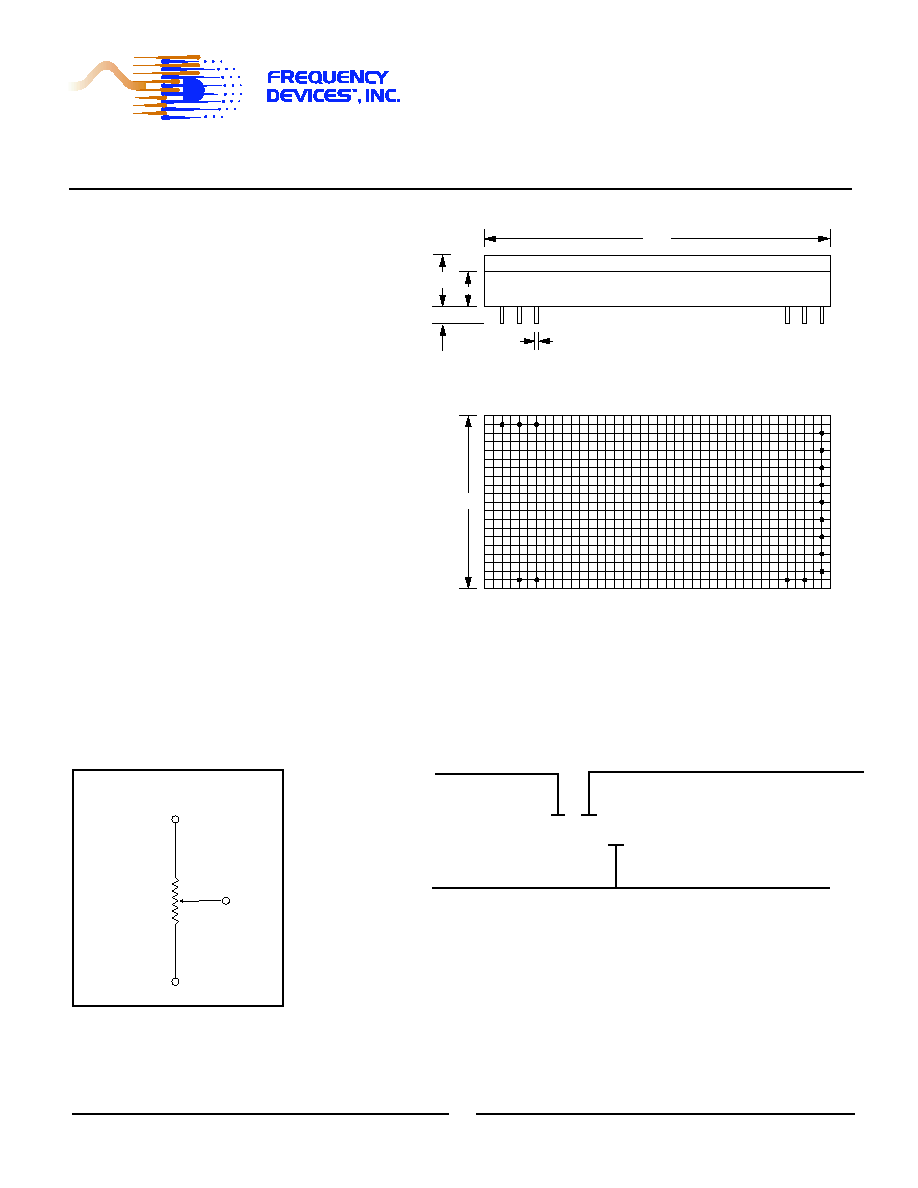
Pin-Out and Package Data
Ordering Information
We hope the information given here will be helpful. The information is based on data and our best knowledge, and we consider the information to be true and accurate. Please read all statements,
recommendations or suggestions herein in conjunction with our conditions of sale which apply to all goods supplied by us. We assume no responsibility for the use of these statements,
recommendations or suggestions, nor do we intend them as a recommendation for any use which would infringe any patent or copyright.
IN-00854-01
DC Offset Adjustment
± Vs
- Vs
20 k
W
(Cermet)
Do not connect
if trim is not
required.
OS
Analog Input Characteristics
1
Impedance
10 k
W
min.
Voltage Range
±
10 Vpeak
Max. Safe Voltage
±
Vs
Analog Output Characteristics
Impedance (Closed Loop)
1
1
W
typ.
10
W
max.
Linear Operating Range
±
10V
Maximum Current
2
±
2 mA
Offset Voltage
3
2
2 mV typ.
20 mV max.
Offset Temp. Coeff.
50
mV/∞C
Power Supply (
±
V)
Rated Voltage
±
15 Vdc
Operating Range
±
12 to
±
18 Vdc
Maximum Safe Voltage
±
18 Vdc
Quiescent Current
4-Pole
±
13 mA typ.
±
20 mA max.
Temperature
Operating
-2
0 to +70∞C
Storage
-25 to +85∞C
Notes:
1. Input and output signal voltage referenced to supply common.
2. Output is short circuit protected to common.
DO NOT CONNECT TO ±Vs.
3. Adjustable to zero.
4. Units operate with or without offset pin connected.
854L8B-3
Transfer Function
B - Butterworth
L - Bessel
Y2 - Chebychev (0.2 dB Ripple)
Y5 - Chebychev (0.2 dB Ripple)
Filter Type
L - Low Pass
H - High Pass
Ordering Information
25 Locust St, Haverhill, Massachusetts 01830 ∑ Tel: 800/252-7074, 978/374-0761 ∑ FAX: 978/521-1839
e-mail: sales@freqdev.com ∑ Web Address: http://www.freqdev.com
Model Tuning Minimum
Number
Range (Hz)
Step(Hz)
Case
1
0.1 to 25.6
0.1
M-2
2
1.0 to 256
1.0
M-2
3
10 to 2560
10
M-1
4
100 to 25.6k
100
M-1
5
200 to 51.2k
200
M-1
6
400 to 102.4k
400
M-1
Model Number
e.g.,
Side View
+Vs
OUT
-Vs
D
D
D
D
GND
D
D
D
D
C
P
IN
2.00
0.4
0.6
4.00
Bottom View
M-1
M-2
0.2 min
0.04 Dia.
Os
4
5
3
2
1
0
6
7
4
Filter Mounting Assembly-See FMA-03A
5
Pin-Out & Package Data