
Ampson Technology, Inc.
A277
1/6 12/26/2001 REV.1.0
COMPLEMENTARY OUTPUT HALL EFFECT
LATCHED SINK DRIVER
FEATURES
!
On-chip Hall sensor with two different sensitivity and hysteresis settings for A277.
!
Internal bandgap regulator allows temperature compensated operations and a wide
operating voltage range.
!
High output sinking capability up to 400mA for driving large load.
!
Lower current change rate reduces the peak output voltages during switching.
!
Build in protection diode for chip reverse power connecting.
!
Available in die form or rugged low profile 4 pin SIP packages.
GENERAL DESCRIPTION
A277 are integrated Hall sensors with output drivers designed for electronic commutation
of brushless DC motor applications. The device includes an on-chip Hall voltage generator
for magnetic sensing, a comparator that amplifies the Hall voltage, and a Schmitt trigger to
provide switching hysteresis for noise rejection, and complementary open-collector drivers
for sinking large current loads. An internal bandgap regulator is used to provide
temperature compensated supply voltage for internal circuits and allows a wide operating
supply range.
If a magnetic flux density larger than threshold Bop, DO is turned on(low) and DOB is
turned off (high). The output state is held until a magnetic flux density reversal falls below
Brp causing DO to be turned off and DOB turned on.
A277 are rated for operation over temperature range from -20
o
C to 85
o
C and voltage
range from 3.5V to 20V. The devices are available in low cost die forms or rugged 4 pin
SIP packages.

Ampson Technology, Inc.
A277
2/6 12/26/2001 REV.1.0
APPLICATIONS
!
Brushless DC Motor
!
Brushless DC Fan
!
Revolution Counting
!
Speed Measurement
FUNCTIONAL BLOCK DIAGRAM
HALL
SENSOR
2 OUTPUT(DO)
3 OUTPUT(DOB)
4 VSS
REG.
1
VCC
PIN DESCRIPTION
277
XXX
1 2
4
3
1 : VCC
2 : DO
3 : D0B
4 : VSS
XXX : DATE CODE ( ex : 52Z )
52 : WEEK ( ex=>52:52 WEEK . 35:35 WEEK )
Z : YEAR ( ex=>Z:DC2001 , Y:DC2002 , X:DC2003 )
REMARK :
Name P/I/O
Pin
#
Description
Vcc
P 1
Positive Power Supply
DO
O 2
Output Pin
DOB
O 3
Output Pin
Vss
P 4
Ground
Ampson Technology, Inc.
A277
3/6 12/26/2001 REV.1.0
ABSOLUTE MAXIMUM RATING
( at Ta=25
o
C )
Supply Voltage, Vcc --------------------------------- 20V
Reverse V
CC
Polarity Voltage, V
RCC
-------------- -35V
Magnetic flux density, B ---------------------------- Unlimited
Output OFF Voltage, Vce -------------------------- 50V(Note 1)
Output ON Current, Ic
Continuous -------------------------------- 400mA
Hold-------- --------------------------------- 500mA
Peak (Start Up) --------------------------- 700mA
Operating Temperature Range,
Ta -------------------------------------------- (-20
o
C to +85
o
C)
Storage Temperature Range,
Ts--------------------------------------------- (-65
o
C to +150
o
C)
Package Power Dissipation,
Pd -------------------------------------------- 500mW
Maximum Junction Temp , Tj----------------------- 175
o
C
(Note1) Output Zener protection voltage.
ELECTRICAL CHARACTERISTICS
( Ta =+25
o
C , Vcc=4.0V to 20V )
Characteristic Symbol Conditions Min
Typ
Max
Units
Low Supply Voltage
Vce
Vcc=3.5V, IL=100mA
--
0.4
--
V
Supply
Voltage
Vcc --
3.5 --
20 V
Output Saturation Voltage Vce(sat) Vcc=14V, IL=300mA
-- 300 600 mV
Output Leakage Current
Icex
Vce=14V, Vcc=14V
-- < 0.1 10
uA
Supply Current
Icc
Vcc=20V, Output Open --
13
20
mA
Output Rise Time
tr
Vcc=14V, RL=820
,
CL=20pF
-- 3.0
10 us
Output Falling Time
tf
Vcc=14V, RL=820
,
CL=20pF
-- 0.3 1.5 us
Switch Time Differential
t
Vcc=14V, RL=820
,
CL=20pF
-- 3.0
10 us
Ampson Technology, Inc.
A277
4/6 12/26/2001 REV.1.0
MAGNETIC CHARACTERISTICS
Characteristic Symbol
Ta=+25
o
C
Min Max
Ta=0
o
C to 70
o
C
Min Max
Units
Operate Point
Bop 0 70 0 70 G
Release Point
Brp
-70
0
-70
0
G
Hysteresis
Bhys 40 110 20 140 G
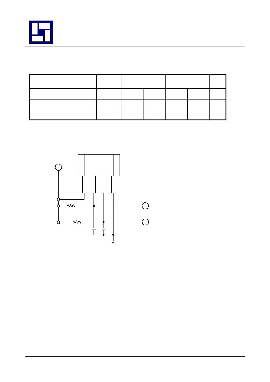
TEST CIRCUIT
CL1
CL2
14V
Vout1(DO)
Vout2(DOB)
RL1=RL2=820 Ohm
CL1=CL2=20 pF
RL2
RL1

Ampson Technology, Inc.
A277
5/6 12/26/2001 REV.1.0
HYSTERESIS CHARACTERISTICS
12
10
8
6
4
2
OFF
OP
RP
ON
Output Voltage in Volts
12
10
8
6
4
2
OP
ON
OFF
RP
Output Voltage in Volts
-200
200
100
-100
0
-200
200
100
-100
0
A277
Magnetic Flux Density in Gauss
Magnetic Flux Density in Gauss
DO
DOB
Power Dissipation VS. Environment Temperature
Ta (
o
C)
25 50 60 70 80 85 90 95 100 105 110 115 120
Pd (mW) 550 525 515 505 485 475 465 455 445 425 405 385 365
NoteTO92 4 pin (SIP-4L) package.
P o w e r D is s ip a tio n C u rv e
1 0 0
2 0 0
3 0 0
4 0 0
5 0 0
6 0 0
0
2 5
5 0
7 5
1 0 0
1 2 5
1 5 0
T a (�C )
P d (m W )

Ampson Technology, Inc.
A277
6/6 12/26/2001 REV.1.0
PACKAGE INFORMATION
Top
View
Marking
Site
0.7mm
1.482mm
1
2
3
4
Active Area Depth
Package Sensor Location
1.96mm
Top
View
PACKAGE DIMENSION
14.25mm
+/-1.25mm
3
o
-5
o
5
o
-7
o
0.85mm
+/-0.1mm
1.55mm
+/-0.1mm
0.38mm
+/-0.03mm
5.22mm
+/-0.1mm
4.20mm
+/-0.1mm
3.65mm
+/-0.1mm
1.27mm
+/-0.03mm
0.38mm
+/-0.03mm
0.46mm
+/-0.03mm
3
o
-5
o
5
o
-7
o
0.30mm
+/-0.1mm
Marking
Site
3.81mm
+/-0.03mm
277
XXX
REMARK: XXX(DATE CODE)