 | –≠–ª–µ–∫—Ç—Ä–æ–Ω–Ω—ã–π –∫–æ–º–ø–æ–Ω–µ–Ω—Ç: AAT8660D | –°–∫–∞—á–∞—Ç—å:  PDF PDF  ZIP ZIP |
Advanced Analog Technology, Inc.
≠
≠
≠
Advanced Analog Technology, Inc
.
≠
Page 1 of 24 V 1.0
AAT8660 Series
Details are subject to change without notice.
ONE-CELL LI-ION BATTERY PROTECTION IC
FEATURES
Ideal for One-Cell Rechargeable Li-Ion
Battery Packs
High Accuracy Voltage Detection
Low Current Consumption:
A
3
µ
Supply Current (Typical)
A
1
.
0
µ
Shutdown Current
3-Level Over Current Detection:
Over-Current Level 1 /Over Current Level 2 /
Short Circuit
Wide Operating Temperature Range:
C
85
to
C
40
o
o
+
-
Small SOT26 Package
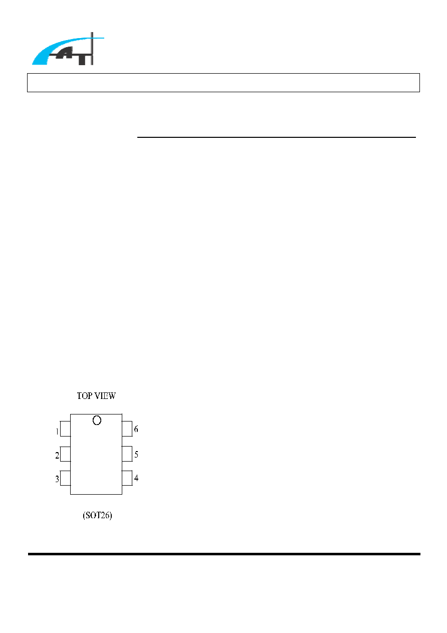
PIN CONFIGURATION
NULL
out
D
VN
out
C
GND
DD
V
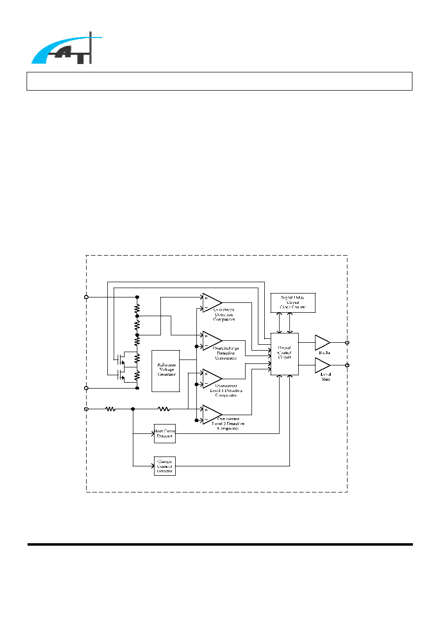
GENERAL DESCRIPTION
The AAT8660 series are designed to protect
one-cell rechargeable Li-Ion battery pack against
over-charge, over-discharge, over-current and
short circuit. They use CMOS process to provide
high accuracy voltage detection and low current
consumption.
Each of the AAT8660 devices incorporates
voltage comparators, bandgap reference voltage
generator, signal delay circuit, short circuit
detector, and digital control circuit.
In the charge process, when the battery voltage is
charged to a value greater than
1
C
V (Over-Charge
Threshold Voltage), the output of
out
C
pin
switches to the low level, i.e., the
VN
pin level.
The output of
out
C
pin will switch to high level
when the battery voltage falls lower than V
C2
(Over-Charge Release Voltage), or when the
charger is disconnected from the battery pack and
the battery voltage level ranges between V
C1
and
V
C2
.
During the discharge process, when the battery
voltage drops to a value lower than
1
D
V
(Over-Discharge Threshold Voltage), the output
of
out
D
pin switches to low level immediately
after the internal delay time elapses. The output
of
out
D
pin will switch to high level when the
battery voltage is at a level higher than
2
D
V
(Over-Discharge Release Voltage).
Advanced Analog Technology, Inc.
≠
≠
≠
Advanced Analog Technology, Inc
.
≠
Page 2 of 24 V 1.0
AAT8660 Series
Over current level 1 voltage (
1
OC
V
) is used to
monitor the amount of discharge current. If the
discharge current is high enough to cause VN pin
voltage increase to a value greater than
1
OC
V
, the
output of
out
D
pin will switch to a low level
after a delay time
1
OC
t
. If the load is removed
from battery pack, the output of
out
D
will
change to a high level again.
The mechanism of short circuit protection is
identical to a discharge current. If the short circuit
current is high enough to cause VN pin voltage
increase to greater than
short
V
, the output of
out
D
pin will move to the low level after a delay
time
short
t
, and the output of
out
D
level will
change to high when the load is removed from
battery pack.
BLOCK DIAGRAM:
DD
V
GND
VN
out
D
out
C
Advanced Analog Technology, Inc.
≠
≠
≠
Advanced Analog Technology, Inc
.
≠
Page 3 of 24 V 1.0
AAT8660 Series
PIN DESCRIPTION
PIN NO NAME I/O
DESCRIPTION
1
out
D
O Discharge Control Pin which Connects to External MOSFET Gate
2
VN
I
Voltage Detection Pin between VN and GND
3
out
C
O Charge Control Pin which Connects to External MOSFET Gate.
4
NULL
Null Pad.
5
DD
V
I
Power Supply Input Pin
6
GND
I Ground
ABSOLUTE MAXIMUM RATINGS
CHARACTERISTICS SYMBOL VALUE UNIT
Supply Voltage
DD
V
3
.
0
-
to 8.0
V
VN Pin Input Voltage
VN
V
20
V
DD
-
to
3
.
0
V
DD
+
V
out
D Pin Output Voltage
Dout
V
3
.
0
-
to 3
.
0
V
DD
+
V
out
C Pin Output Voltage
Cout
V
3
.
0
V
VN
-
to
3
.
0
V
DD
+
V
Power Dissipation
d
P
150
mW
Operating Temperature Range
C
T
40
- to +85
C
o
Storage Temperature Range
storage
T
40
- to +125
C
o
RECOMMENDED OPERATING CONDITIONS
TEST
CONDITION
MIN
MAX
UNIT
Supply Voltage,
DD
V
Voltage Defined as
DD
V
to GND
1.5 7.0 V
out
D Output Voltage
GND
DD
V
V
out
C Output Voltage
VN
DD
V
V
OPERATION VOLTAGE AND OPERATION CURRENT
PARAMETER
TEST CONDITION
MIN TYP MAX
UNIT
Supply Current at Normal Operation
Mode
DD
V =3.3V; VN=0V; GND=0V
3.0
6.0 A
µ
Standby Current at Power Down Mode
- -
0.1
A
µ
Operation Voltage between
DD
V and
VN
1.5 20.0
V
Advanced Analog Technology, Inc.
≠
≠
≠
Advanced Analog Technology, Inc
.
≠
Page 4 of 24 V 1.0
AAT8660 Series
AAT8660A DETECTION VOLTAGE AND DELAY TIME (
C
25
o
)
PARAMETER
SYMBOL
TEST CONDITION
MIN
TYP MAX
UNIT
Over Charge Threshold Voltage
1
C
V
Detect Rising Edge of Supply
Voltage
4.275 4.325 4.375 V
Over Charge Release Voltage
2
C
V
Detect Falling Edge of Supply
Voltage
V
C1
-0.35 V
C1
-0.25 V
C1
-0.15
V
Over Discharge Threshold
Voltage
1
D
V
Detect Falling Edge of Supply
Voltage
2.420 2.500 2.580 V
Over Discharge Release Voltage
2
D
V
Detect Rising Edge of Supply
Voltage
V
D1
+0.3
V
D1
+0.4 V
D1
+0.5
V
Over Charge Delay Time
1
C
t 3.6V
V
DD
=
to 4.5V
0.700 1.000 1.300 s
Over Discharge Delay Time
1
D
t V
6
.
3
V
DD
=
to 2.4V
87.5 125.0 162.5 ms
Over Current Level 1 Detection
Voltage
1
OC
V
Detect Rising Edge of "VN" Pin
Voltage (
out
D Response with t
OC1
Delay Time)
130 150 170 mV
Over Current Level 2 Detection
Voltage
2
OC
V
Detect Rising Edge of "VN"
Pin Voltage (
out
D Response
with t
OC2
Delay Time)
400 500 600 mV
Short Circuit Detection Voltage
short
V
V
0
.
3
V
DD
=
, Detect Rising Edge
of "VN" Pin Voltage (
out
D
Response with
short
t
Delay
Time)
7
.
1
V
DD
-
3
.
1
V
DD
-
9
.
0
V
DD
-
V
Over Current Level 1 Detection
Delay Time
1
OC
t
V
0
.
3
V
DD
=
5.6
8.0
10.4
ms
Over Current Level 2 Detection
Delay Time
2
OC
t
Room Temp.
Low or High Temp.
V
0
.
3
V
DD
=
1.4
1.1
2.0
2.0
2.6
3.4
ms
ms
Short Circuit Detection Delay
Time
short
t
V
0
.
3
V
DD
=
10 50 s
µ
Charger Detection Voltage
CHR
V
Detect Rising Edge of "
out
D
"
Pin Voltage (when V
D1
V
DD
V
D2
)
0
.
2
-
3
.
1
-
6
.
0
-
V
out
C High Level Resistance
COH
R
V
5
.
3
V
DD
=
; V
0
.
3
C
out
=
;
V
0
VN
=
1 2 10
k
out
C
Low Level Resistance
COL
R
V
5
.
4
V
DD
=
;
V
5
.
0
C
out
=
;
V
0
VN
=
150 602 2,380
k
out
D High Level Resistance
DOH
R
V
5
.
3
V
DD
=
;
V
0
.
3
D
out
=
;
V
0
VN
=
2.5 5.0 10.0
k
out
D Low Level Resistance
DOL
R
V
8
.
1
V
DD
=
;
V
5
.
0
D
out
=
;
V
8
.
1
VN
=
2.5 5.0 10.0
k
Internal Resistance between VN
and
DD
V
VND
R
V
8
.
1
V
DD
=
; V
0
VN
=
100 300 900
k
Internal Resistance between VN
and GND
VNG
R
V
5
.
3
V
DD
=
; V
5
.
3
VN
=
10 20 40
k
Advanced Analog Technology, Inc.
≠
≠
≠
Advanced Analog Technology, Inc
.
≠
Page 5 of 24 V 1.0
AAT8660 Series
AAT8660B DETECTION VOLTAGE AND DELAY TIME (25)
PARAMETER
SYMBOL
TEST CONDITION
MIN TYP MAX
UNIT
Over Charge Threshold Voltage
1
C
V
Detect Rising Edge of Supply
Voltage
4.300 4.350 4.400 V
Over Charge Release Voltage
2
C
V
Detect Falling Edge of Supply
Voltage
V
C1
-0.30 V
C1
-0.20 V
C1
-0.10
V
Over Discharge Threshold
Voltage
1
D
V
Detect Falling Edge of Supply
Voltage
2.220 2.300 2.380 V
Over Discharge Release Voltage
2
D
V
Detect Rising Edge of Supply
Voltage
V
D1
+0.6 V
D1
+0.7 V
D1
+0.8
V
Over Charge Delay Time
1
C
t V
6
.
3
V
DD
=
to 4.5V
0.088 0.125 0.163 s
Over Discharge Delay Time
1
D
t V
6
.
3
V
DD
=
to 2.4V
22.4 32.0 41.6 ms
Over Current Level 1 Detection
Voltage
1
OC
V
Detect Rising Edge of "VN" Pin
Voltage (
out
D Response with
1
OC
t
Delay Time)
130 150 170 mV
Over Current Level 2 Detection
Voltage
2
OC
V
Detect Rising Edge of "VN"
Pin Voltage (
out
D Response
with t
OC2
Delay Time)
400 500 600 mV
Short Circuit Detection Voltage
short
V
V
0
.
3
V
DD
=
, Detect Rising Edge
of "VN" Pin Voltage
(
out
D Response with
short
t
Delay Time)
7
.
1
V
DD
-
3
.
1
V
DD
-
9
.
0
V
DD
-
V
Over Current Level 1 Detection
Delay Time
1
OC
t
V
0
.
3
V
DD
=
2.8
4.0 5.2 ms
Over Current Level 2 Detection
Delay Time
2
OC
t
Room Temp.
Low or High Temp.
V
0
.
3
V
DD
=
1.4
1.1
2.0
2.0
2.6
3.4
ms
ms
Short Circuit Detection Delay
Time
short
t
V
0
.
3
V
DD
=
10 50 s
µ
Charger Detection Voltage
CHR
V
Detect Rising Edge of "
out
D "
Pin Voltage
(when V
D1
V
DD
V
D2
)
0
.
2
-
3
.
1
-
6
.
0
-
V
out
C High Level Resistance
COH
R
V
5
.
3
V
DD
=
;
V
0
.
3
C
OUT
=
;
V
0
VN
=
1 2 10
k
out
C Low Level Resistance
COL
R
V
5
.
4
V
DD
=
;
V
5
.
0
C
OUT
=
;
V
0
VN
=
150 602 2,380
k
out
D High Level Resistance
DOH
R
V
5
.
3
V
DD
=
;
V
0
.
3
D
out
=
;
V
0
VN
=
2.5 5.0 10.0
k
out
D Low Level Resistance
DOL
R
V
8
.
1
V
DD
=
;
V
5
.
0
D
out
=
;
V
8
.
1
VN
=
2.5 5.0 10.0
k
Internal Resistance between VN
and
DD
V
VND
R
V
8
.
1
V
DD
=
; V
0
VN
=
100 300 900
k
Internal Resistance between VN
and GND
VNG
R
V
5
.
3
V
DD
=
; V
5
.
3
VN
=
10 20 40
k

Advanced Analog Technology, Inc.
≠
≠
≠
Advanced Analog Technology, Inc
.
≠
Page 6 of 24 V 1.0
AAT8660 Series
AAT8660C DETECTION VOLTAGE AND DELAY TIME (25)
PARAMETER
SYMBOL
TEST CONDITION
MIN
TYP MAX UNIT
Over Charge Threshold Voltage
1
C
V
Detect Rising Edge of Supply
Voltage
4.250 4.300 4.350 V
Over Charge Release Voltage
2
C
V
Detect Falling Edge of Supply
Voltage
V
C1
-0.30 V
C1
-0.20 V
C1
-0.10
V
Over Discharge Threshold
Voltage
1
D
V
Detect Falling Edge of Supply
Voltage
2.220 2.300 2.380 V
Over Discharge Release Voltage
2
D
V
Detect Rising Edge of Supply
Voltage
V
D1
-0.08
V
D1
V
D1
+0.08
V
Over Charge Delay Time
1
C
t V
6
.
3
V
DD
=
to 4.5V
0.700 1.000 1.300 s
Over Discharge Delay Time
1
D
t V
6
.
3
V
DD
=
to 2.4V
87.5 125.0 162.5 ms
Over Current Level 1 Detection
Voltage
1
OC
V
Detect Rising Edge of "VN" Pin
Voltage (
out
D Response with t
OC1
Delay Time)
80 100 120 mV
Over Current Level 2 Detection
Voltage
2
OC
V
Detect Rising Edge of "VN" Pin
Voltage (
out
D Response with
t
OC2
Delay Time)
400 480 600 mV
Short Circuit Detection Voltage
short
V
V
0
.
3
V
DD
=
, Detect Rising Edge
of "VN" Pin Voltage
(
out
D Response with
short
t
Delay Time)
7
.
1
V
DD
-
3
.
1
V
DD
-
9
.
0
V
DD
-
V
Over Current Level 1 Detection
Delay Time
1
OC
t
V
0
.
3
V
DD
=
5.6
8.0
10.4
ms
Over Current Level 2 Detection
Delay Time
2
OC
t
Room Temp.
Low or High Temp.
V
0
.
3
V
DD
=
1.4
1.1
2.0
2.0
2.6
3.4
ms
ms
Short Circuit Detection Delay
Time
short
t
V
0
.
3
V
DD
=
10 50
s
µ
Charger Detection Voltage
CHR
V
Detect Rising Edge of "
out
D
"
Pin Voltage
(when V
D1
V
DD
V
D2
)
0
.
2
-
3
.
1
-
6
.
0
-
V
out
C High Level Resistance
COH
R
V
5
.
3
V
DD
=
;
V
0
.
3
C
out
=
;
V
0
VN
=
1 2 10
k
out
C Low Level Resistance
COL
R
V
5
.
4
V
DD
=
;
V
5
.
0
C
out
=
;
V
0
VN
=
150 602 2,380
k
out
D High Level Resistance
DOH
R
V
5
.
3
V
DD
=
;
V
0
.
3
D
out
=
;
V
0
VN
=
2.5 5.0 10.0
k
out
D Low Level Resistance
DOL
R
V
8
.
1
V
DD
=
;
V
5
.
0
D
out
=
;
V
8
.
1
VN
=
2.5 5.0 10.0
k
Internal Resistance between VN
and
DD
V
VND
R
V
8
.
1
V
DD
=
;
V
0
VN
=
100 300 900
k
Internal Resistance between VN
and GND
VNG
R
V
5
.
3
V
DD
=
;
V
5
.
3
VN
=
10 20 40
k
Advanced Analog Technology, Inc.
≠
≠
≠
Advanced Analog Technology, Inc
.
≠
Page 7 of 24 V 1.0
AAT8660 Series
AAT8660D DETECTION VOLTAGE AND DELAY TIME (25)
PARAMETER
SYMBOL
TEST CONDITION
MIN TYP MAX
UNIT
Over Charge Threshold Voltage
1
C
V
Detect Rising Edge of Supply
Voltage
4.230 4.280 4.330 V
Over Charge Release Voltage
2
C
V
Detect Falling Edge of Supply
Voltage
V
C1
-0.30 V
C1
-0.20 V
C1
-0.10
V
Over Discharge Threshold
Voltage
1
D
V
Detect Falling Edge of Supply
Voltage
2.201 2.281 2.361 V
Over Discharge Release Voltage
2
D
V
Detect Rising Edge of Supply
Voltage
V
D1
-0.08 V
D1
V
D1
+0.08
V
Over Charge Delay Time
1
C
t V
6
.
3
V
DD
=
to 4.5V
0.700 1.000 1.300 s
Over Discharge Delay Time
1
D
t V
6
.
3
V
DD
=
to 2.4V
87.5 125.0 162.5 ms
Over Current Level 1 Detection
Voltage
1
OC
V
Detect Rising Edge of "VN" Pin
Voltage (
out
D
Response With
t
OC1
Delay Time)
110 130 150
mV
Over Current Level 2 Detection
Voltage
2
OC
V
Detect Rising Edge of "VN"
Pin Voltage (
out
D
Response
with
2
OC
t
Delay Time)
400 490 600
mV
Short Circuit Detection Voltage
short
V
V
0
.
3
V
DD
=
, Detect Rising Edge
of "VN" Pin Voltage (
out
D
Response with
short
t
Delay Time)
7
.
1
V
DD
-
3
.
1
V
DD
-
9
.
0
V
DD
-
V
Over Current Level 1 Detection
Delay Time
1
OC
t
V
0
.
3
V
DD
=
5.6 8.0 10.4
ms
Over Current Level 2 Detection
Delay Time
2
OC
t
Room Temp.
Low or High Temp.
V
0
.
3
V
DD
=
1.4
1.1
2.0
2.0
2.6
3.4
ms
ms
Short Circuit Detection Delay
Time
short
t
V
0
.
3
V
DD
=
10 50
µs
Charger Detection Voltage
CHR
V
Detect Rising Edge of "
out
D
"
Pin Voltage
(when V
D1
V
DD
V
D2
)
0
.
2
-
3
.
1
-
6
.
0
-
V
out
C High Level Resistance
COH
R
V
5
.
3
V
DD
=
;
V
0
.
3
C
out
=
;
V
0
VN
=
1 2 10
k
out
C Low Level Resistance
COL
R
V
5
.
4
V
DD
=
;
V
5
.
0
C
out
=
;
V
0
VN
=
150 602 2,380
k
out
D High Level Resistance
DOH
R
V
5
.
3
V
DD
=
;
V
0
.
3
D
out
=
;
V
0
VN
=
2.5 5.0 10.0
k
out
D Low Level Resistance
DOL
R
V
8
.
1
V
DD
=
; V
5
.
0
D
out
=
;
V
8
.
1
VN
=
2.5 5.0 10.0
k
Internal Resistance between VN
and
DD
V
VND
R
V
8
.
1
V
DD
=
; VN=0V
100 300 900
k
Internal Resistance between VN
and GND
VNG
R
V
5
.
3
V
DD
=
; V
5
.
3
VN
=
10 20 40
k
Advanced Analog Technology, Inc.
≠
≠
≠
Advanced Analog Technology, Inc
.
≠
Page 8 of 24 V 1.0
AAT8660 Series
AAT8660E DETECTION VOLTAGE AND DELAY TIME (25)
PARAMETER
SYMBOL
TEST CONDITION
MIN TYP MAX
UNIT
Over Charge Threshold Voltage
1
C
V
Detect Rising Edge of Supply
Voltage
4.230 4.280 4.330 V
Over Charge Release Voltage
2
C
V
Detect Falling Edge of Supply
Voltage
V
C1
-0.30 V
C1
-0.20 V
C1
-0.10
V
Over Discharge Threshold
Voltage
1
D
V
Detect Falling Edge of Supply
Voltage
2.201 2.281 2.361 V
Over Discharge Release Voltage
2
D
V
Detect Rising Edge of Supply
Voltage
V
D1
+0.5
V
D1
+0.6 V
D1
+0.7
V
Over Charge Delay Time
1
C
t V
6
.
3
V
DD
=
to 4.5V
0.700 1.000 1.300 s
Over Discharge Delay Time
1
D
t V
6
.
3
V
DD
=
to 2.4V
87.5 125.0 162.5 ms
Over Current Level 1 Detection
Voltage
1
OC
V
Detect Rising Edge of "VN" Pin
Voltage (
out
D
Response with
1
OC
t
Delay Time)
80 100 120
mV
Over Current Level 2 Detection
Voltage
2
OC
V
Detect Rising Edge of "VN"
Pin Voltage (
out
D
Response
with
2
OC
t
Delay Time)
400 480 600
mV
Short Circuit Detection Voltage
short
V
V
0
.
3
V
DD
=
, Detect Rising
Edge of "VN" Pin Voltage
(
out
D Response with short
t
Delay Time)
7
.
1
V
DD
-
3
.
1
V
DD
-
9
.
0
V
DD
-
V
Over Current Level 1 Detection
Delay Time
1
OC
t
V
0
.
3
V
DD
=
5.6 8.0 10.4
ms
Over Current Level 2 Detection
Delay Time
2
OC
t
Room Temp.
Low or High Temp.
V
0
.
3
V
DD
=
1.4
1.1
2.0
2.0
2.6
3.4
ms
ms
Short Circuit Detection Delay
Time
short
t
V
0
.
3
V
DD
=
10 50 s
µ
Charger Detection Voltage
CHR
V
Detect Rising Edge of "
out
D
"
Pin Voltage
(when V
D1
V
DD
V
D2
)
-2.0 -1.3 -0.6 V
out
C High Level Resistance
COH
R
3.5V
V
DD
=
;
V
0
.
3
C
out
=
;
0V
VN
=
1 2 10
k
out
C Low Level Resistance
COL
R
4.5V
V
DD
=
;
V
5
.
0
C
out
=
;
0V
VN
=
150 602 2,380
k
out
D High Level Resistance
DOH
R
3.5V
V
DD
=
; V
0
.
3
D
out
=
;
0V
VN
=
2.5 5.0 10.0
k
out
D Low Level Resistance
DOL
R
1.8V
V
DD
=
; V
5
.
0
D
out
=
;
1.8V
VN
=
2.5 5.0 10.0
k
Internal Resistance between VN
and
DD
V
VND
R
1.8V
V
DD
=
; 0V
VN
=
100 300 900
k
Internal Resistance between VN
and GND
VNG
R
3.5V
V
DD
=
; 3.5V
VN
=
10 20 40
k

Advanced Analog Technology, Inc.
≠
≠
≠
Advanced Analog Technology, Inc
.
≠
Page 9 of 24 V 1.0
AAT8660 Series
AAT8660F
DETECTION VOLTAGE AND DELAY TIME (25)
PARAMETER
SYMBOL
TEST CONDITION
MIN TYP MAX UNIT
Over Charge Threshold Voltage
1
C
V
Detect Rising Edge of Supply
Voltage
4.275 4.325 4.375 V
Over Charge Release Voltage
2
C
V
Detect Falling Edge of Supply
Voltage
V
C1
-0.35 V
C1
-0.25 V
C1
-0.15
V
Over Discharge Threshold
Voltage
1
D
V
Detect Falling Edge of Supply
Voltage
2.420 2.500 2.580 V
Over Discharge Release Voltage
2
D
V
Detect Rising Edge of Supply
Voltage
V
D1
+0.3 V
D1
+0.4 V
D1
+0.5
V
Over Charge Delay Time
1
C
t V
6
.
3
V
DD
=
to 4.5V
0.700 1.000 1.300 s
Over Discharge Delay Time
1
D
t V
6
.
3
V
DD
=
to 2.4V
87.5 125.0 162.5 ms
Over Current Level 1 Detection
Voltage
1
OC
V
Detect Rising Edge of "VN" Pin
Voltage (
out
D Response with
1
OC
t
Delay Time)
80 100 120 mV
Over Current Level 2 Detection
Voltage
2
OC
V
Detect Rising Edge of "VN"
Pin Voltage (
out
D Response
with
2
OC
t
Delay Time)
400 480 600 mV
Short Circuit Detection Voltage
short
V
V
0
.
3
V
DD
=
, Detect Rising Edge
of "VN" Pin Voltage (
out
D
Response with short
t
Delay Time)
7
.
1
V
DD
-
3
.
1
V
DD
-
9
.
0
V
DD
-
V
Over Current Level 1 Detection
Delay Time
1
OC
t
V
0
.
3
V
DD
=
5.6 8.0 10.4 ms
Over Current Level 2 Detection
Delay Time
2
OC
t
Room Temp.
Low or High Temp.
V
0
.
3
V
DD
=
1.4
1.1
2.0
2.0
2.6
3.4
ms
ms
Short Circuit Detection Delay
Time
short
t
V
0
.
3
V
DD
=
10
50 s
µ
Charger Detection Voltage
CHR
V
Detect Rising Edge of "
out
D
"
Pin Voltage
(When V
D1
V
DD
V
D2
)
0
.
2
-
3
.
1
-
6
.
0
-
V
out
C High Level Resistance
COH
R
V
5
.
3
V
DD
=
;
V
0
.
3
C
out
=
;
V
0
VN
=
1 2 10
k
out
C Low Level Resistance
COL
R
V
5
.
4
V
DD
=
; V
5
.
0
C
out
=
;
V
0
VN
=
150 602
2,380
k
out
D High Level Resistance
DOH
R
V
5
.
3
V
DD
=
;
V
0
.
3
D
out
=
;VN=0V
2.5 5.0 10.0
k
out
D Low Level Resistance
DOL
R
V
8
.
1
V
DD
=
;
V
5
.
0
D
out
=
;VN=1.8V
2.5 5.0 10.0
k
Internal Resistance between VN
and
DD
V
VND
R
V
8
.
1
V
DD
=
; V
0
VN
=
100 300 900
k
Internal Resistance between VN
and GND
VNG
R
V
5
.
3
V
DD
=
; VN=3.5V
10 20 40 k

Advanced Analog Technology, Inc.
≠
≠
≠
Advanced Analog Technology, Inc
.
≠
Page 10 of 24 V 1.0
AAT8660 Series
AAT8660G DETECTION VOLTAGE AND DELAY TIME (25)
PARAMETER
SYMBOL
TEST CONDITION
MIN TYP MAX UNIT
Over Charge Threshold Voltage
1
C
V
Detect Rising Edge of Supply
Voltage
4.300 4.350 4.400 V
Over Charge Release Voltage
2
C
V
Detect Falling Edge of Supply
Voltage
V
C1
-0.30 V
C1
-0.20 V
C1
-0.10
V
Over Discharge Threshold
Voltage
1
D
V
Detect Falling Edge of Supply
Voltage
2.220 2.300 2.380 V
Over Discharge Release Voltage
2
D
V
Detect Rising Edge of Supply
Voltage
V
D1
+0.6
V
D1
+0.7 V
D1
+0.8
V
Over Charge Delay Time
1
C
t V
6
.
3
V
DD
=
to 4.5V
0.088 0.125 0.163 s
Over Discharge Delay Time
1
D
t V
6
.
3
V
DD
=
to 2.4V
22.4 32.0 41.6 ms
Over Current Level 1 Detection
Voltage
1
OC
V
Detect Rising Edge of "VN" Pin
Voltage (
out
D Response with
t
OC1
Delay Time)
180 200 220 mV
Over Current Level 2 Detection
Voltage
2
OC
V
Detect Rising Edge of "VN"
Pin Voltage (
out
D Response
with t
OC2
Delay Time)
400 510 600 mV
Short Circuit Detection Voltage
short
V
V
0
.
3
V
DD
=
, Detect Rising Edge
of "VN" Pin Voltage (
out
D
Response with
short
t
Delay Time)
7
.
1
V
DD
-
3
.
1
V
DD
-
9
.
0
V
DD
-
V
Over Current Level 1 Detection
Delay Time
1
OC
t
V
0
.
3
V
DD
=
2.8
4
5.2
ms
Over Current Level 2 Detection
Delay Time
2
OC
t
Room Temp.
Low or High Temp.
V
0
.
3
V
DD
=
1.4
1.1
2.0
2.0
2.6
3.4
ms
ms
Short Circuit Detection Delay
Time
short
t
V
0
.
3
V
DD
=
10
50 s
µ
Charger Detection Voltage
CHR
V
Detect Rising Edge of "
out
D
"
Pin Voltage(when V
D1
V
DD
V
D2
)
0
.
2
-
3
.
1
-
6
.
0
-
V
out
C High Resistance Level
COH
R
V
5
.
3
V
DD
=
;
V
0
.
3
C
out
=
;VN=0V
1 2 10
k
out
C Low Resistance Level
COL
R
V
5
.
4
V
DD
=
;
V
5
.
0
C
out
=
;VN=0V
150 602
2,380
k
out
D High Resistance Level
DOH
R
V
5
.
3
V
DD
=
;
V
0
.
3
D
out
=
;VN=0V
2.5 5.0 10.0
k
out
D Low Resistance Level
DOL
R
V
8
.
1
V
DD
=
;
V
5
.
0
D
out
=
;VN=1.8V
2.5 5.0 10.0
k
Internal Resistance between VN
and
DD
V
VND
R
V
8
.
1
V
DD
=
; VN=0V
100 300 900
k
Internal Resistance between VN
and GND
VNG
R
3.5V
V
DD
=
; VN=3.5V
10 20 40
k
Advanced Analog Technology, Inc.
≠
≠
≠
Advanced Analog Technology, Inc
.
≠
Page 11 of 24 V 1.0
AAT8660 Series
AAT8660H DETECTION VOLTAGE AND DELAY TIME (25)
PARAMETER
SYMBOL
TEST CONDITION
MIN TYP MAX
UNIT
Over Charge Threshold Voltage
1
C
V
Detect Rising Edge of Supply
Voltage
4.250 4.300 4.350 V
Over Charge Release Voltage
2
C
V
Detect Falling Edge of Supply
Voltage
V
C1
-0.30 V
C1
-0.20 V
C1
-0.10
V
Over Discharge Threshold
Voltage
1
D
V
Detect Falling Edge of Supply
Voltage
2.220 2.300 2.380 V
Over Discharge Release Voltage
2
D
V
Detect rising Edge of Supply
Voltage
V
D1
-0.08 V
D1
V
D1
+0.08
V
Over Charge Delay Time
1
C
t V
6
.
3
V
DD
=
to 4.5V
0.700 1.000 1.300
s
Over Discharge Delay Time
1
D
t V
6
.
3
V
DD
=
to 2.4V
87.5 125.0 162.5 ms
Over Current Level 1 Detection
Voltage
1
OC
V
Detect Rising Edge of "VN" Pin
Voltage (
out
D Response with
1
OC
t
Delay time)
130 150 170 mV
Over Current Level 2 Detection
Voltage
2
OC
V
Detect rising Edge of "VN"
Pin Voltage (
out
D Response
With
2
OC
t
Delay Time)
400 500 600 mV
Short Circuit Detection Voltage
short
V
V
0
.
3
V
DD
=
, Detect Rising Edge
of "VN" Pin Voltage (
out
D
Response with short
t
Delay
Time)
7
.
1
V
DD
-
3
.
1
V
DD
-
9
.
0
V
DD
-
V
Over Current Level 1 Detection
Delay Time
1
OC
t
V
0
.
3
V
DD
=
5.6 8.0
10.4 ms
Over Current Level 2 Detection
Delay Time
2
OC
t
Room Temp.
Low or High Temp.
V
0
.
3
V
DD
=
1.4
1.1
2.0
2.0
2.6
3.4
ms
ms
Short Circuit Detection Delay
Time
short
t
V
0
.
3
V
DD
=
10 50 s
µ
Charger Detection Voltage
CHR
V
Detect Rising Edge of "
out
D
"
Pin Voltage
(when V
D1
V
DD
V
D2
)
-2.0 -1.3 -0.6 V
out
C High Resistance Level
COH
R
V
5
.
3
V
DD
=
;
V
0
.
3
C
out
=
;VN=0V
1 2 10
k
out
C Low Resistance Level
COL
R
V
5
.
4
V
DD
=
;
V
5
.
0
C
out
=
;VN=0V
150 602 2,380
k
out
D High Resistance Level
DOH
R
V
5
.
3
V
DD
=
;
V
0
.
3
D
out
=
;VN=0V
2.5 5.0 10.0
k
out
D Low Resistance Level
DOL
R
V
8
.
1
V
DD
=
;
V
5
.
0
D
out
=
;VN=1.8V
2.5 5.0 10.0
k
Internal Resistance between VN
and
DD
V
VND
R
V
8
.
1
V
DD
=
; VN=0V
100 300 900
k
Internal Resistance between VN
and GND
VNG
R
V
5
.
3
V
DD
=
; VN=3.5V
10 20 40
k
Advanced Analog Technology, Inc.
≠
≠
≠
Advanced Analog Technology, Inc
.
≠
Page 12 of 24 V 1.0
AAT8660 Series
AAT8660I DETECTION VOLTAGE AND DELAY TIME (25)
PARAMETER
SYMBOL
TEST CONDITION
MIN
TYP MAX UNIT
Over Charge Threshold Voltage
1
C
V
Detect Rising Edge of Supply
Voltage
4.250 4.300 4.350 V
Over Charge Release Voltage
2
C
V
Detect Falling Edge of Supply
Voltage
V
C1
-0.30 V
C1
-0.20 V
C1
-0.10
V
Over Discharge Threshold
Voltage
1
D
V
Detect Falling Edge of Supply
Voltage
2.220 2.300 2.380 V
Over Discharge Release Voltage
2
D
V
Detect Rising Edge of Supply
Voltage
V
D1
-0.08
V
D1
V
D1
+0.08
V
Over Charge Delay Time
1
C
t V
6
.
3
V
DD
=
to 4.5V
0.700 1.000 1.300 s
Over Discharge Delay Time
1
D
t V
6
.
3
V
DD
=
to 2.4V
87.5 125.0 162.5 ms
Over Current Level 1 Detection
Voltage
1
OC
V
Detect Rising Edge of "VN" Pin
Voltage (
out
D Response with
1
OC
t
Delay Time)
110 130 150 mV
Over Current Level 2 Detection
Voltage
2
OC
V
Detect Rising Edge of "VN"
Pin Voltage (
out
D Response
with
2
OC
t
Delay Time)
400 490 600 mV
Short Circuit Detection Voltage
short
V
V
0
.
3
V
DD
=
, Detect Rising Edge
of "VN" Pin Voltage (
out
D
Response with short
t
Delay Time)
7
.
1
V
DD
-
3
.
1
V
DD
-
9
.
0
V
DD
-
V
Over Current Level 1 Detection
Delay Time
1
OC
t
V
0
.
3
V
DD
=
5.6 8.0 10.4 ms
Over Current Level 2 Detection
Delay Time
2
OC
t
Room Temp.
Low or High Temp.
V
0
.
3
V
DD
=
1.4
1.1
2.0
2.0
2.6
3.4
ms
ms
Short Circuit Detection Delay
Time
short
t
V
0
.
3
V
DD
=
10 50 s
µ
Charger Detection Voltage
CHR
V
Detect Rising Edge of "
out
D
"
Pin Voltage
(when V
D1
V
DD
V
D2
)
0
.
2
-
3
.
1
-
6
.
0
-
V
out
C High Resistance Level
COH
R
V
5
.
3
V
DD
=
;
3.0V
C
out
=
;VN=0V
1 2 10
k
out
C Low Resistance Level
COL
R
V
5
.
4
V
DD
=
;
V
5
.
0
C
out
=
;VN=0V
150 602 2,380
k
out
D High Resistance Level
DOH
R
V
5
.
3
V
DD
=
;
V
0
.
3
D
out
=
;VN=0V
2.5 5.0 10.0
k
out
D Low Resistance Level
DOL
R
V
8
.
1
V
DD
=
;
V
5
.
0
D
out
=
;VN=1.8V
2.5 5.0 10.0
k
Internal Resistance between VN
and
DD
V
VND
R
V
8
.
1
V
DD
=
; VN=0V
100 300 900
k
Internal Resistance between VN
and GND
VNG
R
V
5
.
3
V
DD
=
; VN=3.5V
10 20 40 k
Advanced Analog Technology, Inc.
≠
≠
≠
Advanced Analog Technology, Inc
.
≠
Page 13 of 24 V 1.0
AAT8660 Series
AAT8660J DETECTION VOLTAGE AND DELAY TIME (25)
PARAMETER
SYMBOL
TEST CONDITION
MIN TYP MAX UNIT
Over Charge Threshold Voltage
1
C
V
Detect Rising Edge of Supply
Voltage
4.230 4.280 4.330 V
Over Charge Release Voltage
2
C
V
Detect Falling Edge of Supply
Voltage
V
C1
-0.30 V
C1
-0.20 V
C1
-0.10
V
Over Discharge Threshold
Voltage
1
D
V
Detect Falling Edge of Supply
Voltage
2.201 2.281 2.361 V
Over Discharge Release Voltage
2
D
V
Detect Rising Edge of Supply
Voltage
V
D1
-0.08 V
D1
V
D1
+0.08
V
Over Charge Delay Time
1
C
t V
6
.
3
V
DD
=
to 4.5V
0.700 1.000 1.300 s
Over Discharge Delay Time
1
D
t V
6
.
3
V
DD
=
to 2.4V
87.5 125.0 162.5
ms
Over Current Level 1 Detection
Voltage
1
OC
V
Detect Rising Edge of "VN" Pin
Voltage (
out
D Response with
1
OC
t
Delay Time)
180 200 220
mV
Over Current Level 2 Detection
Voltage
2
OC
V
Detect Rising Edge of "VN"
Pin Voltage (
out
D Response
with
2
OC
t
Delay Time)
400 510 600
mV
Short Circuit Detection Voltage
short
V
V
0
.
3
V
DD
=
, Detect Rising Edge
of "VN" Pin Voltage (
out
D
Response with short
t
Delay Time)
7
.
1
V
DD
-
3
.
1
V
DD
-
9
.
0
V
DD
-
V
Over Current Level 1 Detection
Delay Time
1
OC
t
V
0
.
3
V
DD
=
5.6 8.0 10.4
ms
Over Current Level 2 Detection
Delay Time
2
OC
t
Room Temp.
Low or High Temp.
V
0
.
3
V
DD
=
1.4
1.1
2.0
2.0
2.6
3.4
ms
ms
Short Circuit Detection Delay
Time
short
t
V
0
.
3
V
DD
=
10
50
s
µ
Charger Detection Voltage
CHR
V
Detect Rising Edge of "
out
D "
Pin Voltage (when V
D1
V
DD
V
D2
)
-2.0 -1.3 -0.6 V
out
C High Level Resistance
COH
R
V
5
.
3
V
DD
=
;
V
0
.
3
C
out
=
;VN=0V
1 2 10
k
out
C Low Level Resistance
COL
R
V
5
.
4
V
DD
=
;
V
5
.
0
C
out
=
;VN=0V
150 602
2,380
k
out
D High Level Resistance
DOH
R
V
5
.
3
V
DD
=
;
V
0
.
3
D
out
=
;VN=0V
2.5 5.0 10.0
k
out
D Low Level Resistance
DOL
R
V
8
.
1
V
DD
=
;
V
5
.
0
D
out
=
;VN=1.8V
2.5 5.0 10.0
k
Internal Resistance between VN
and
DD
V
VND
R
V
8
.
1
V
DD
=
; VN=0V
100 300 900
k
Internal Resistance between VN
and GND
VNG
R
V
5
.
3
V
DD
=
; VN=3.5V
10 20 40
k
Advanced Analog Technology, Inc.
≠
≠
≠
Advanced Analog Technology, Inc
.
≠
Page 14 of 24 V 1.0
AAT8660 Series
SUMMARY OF AAT8660 DETECTION VOLTAGE AND DELAY TIME (
C
25
o
)
PARAMETER
SYMBOL
DEVICE
MIN TYP MAX
UNIT
Over Charge Threshold Voltage
1
C
V
AAT8660A
4.275 4.325 4.375 V
AAT8660B
4.300
4.350 4.400 V
AAT8660C
4.250
4.300 4.350 V
AAT8660D
4.230
4.280 4.330 V
AAT8660E
4.230
4.280 4.330 V
AAT8660F
4.275
4.325 4.375 V
AAT8660G
4.300
4.350 4.400 V
AAT8660H
4.250
4.300 4.350 V
AAT8660I
4.250
4.300 4.350 V
AAT8660J
4.230
4.280 4.330 V
Over Charge Release Voltage
2
C
V
AAT8660A V
C1
-0.35 V
C1
-0.25 V
C1
-0.15 V
AAT8660B
V
C1
-0.30 V
C1
-0.20 V
C1
-0.10 V
AAT8660C
V
C1
-0.30 V
C1
-0.20 V
C1
-0.10 V
AAT8660D
V
C1
-0.30 V
C1
-0.20 V
C1
-0.10 V
AAT8660E
V
C1
-0.30 V
C1
-0.20 V
C1
-0.10 V
AAT8660F
V
C1
-0.35 V
C1
-0.25 V
C1
-0.15 V
AAT8660G
V
C1
-0.30 V
C1
-0.20 V
C1
-0.10 V
AAT8660H
V
C1
-0.30 V
C1
-0.20 V
C1
-0.10 V
AAT8660I
V
C1
-0.30 V
C1
-0.20 V
C1
-0.10 V
AAT8660J
V
C1
-0.30 V
C1
-0.20 V
C1
-0.10 V
Over Discharge Threshold Voltage
1
D
V
AAT8660A
2.420
2.500 2.580 V
AAT8660B
2.220
2.300 2.380 V
AAT8660C
2.220
2.300 2.380 V
AAT8660D
2.201
2.281 2.361 V
AAT8660E
2.201
2.281 2.361 V
AAT8660F
2.420
2.500 2.580 V
AAT8660G
2.220
2.300 2.380 V
AAT8660H
2.220
2.300 2.380 V
AAT8660I
2.220
2.300 2.380 V
AAT8660J
2.201
2.281 2.361 V
Advanced Analog Technology, Inc.
≠
≠
≠
Advanced Analog Technology, Inc
.
≠
Page 15 of 24 V 1.0
AAT8660 Series
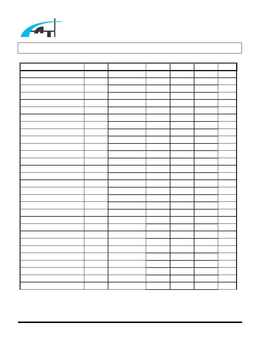
SUMMARY OF AAT8660 DETECTION VOLTAGE AND DELAY TIME (25)
PARAMETER
SYMBOL
DEVICE
MIN TYP MAX
UNIT
Over Discharge Release Voltage
2
D
V
AAT8660A V
D1
+0.3 V
D1
+0.4 V
D1
+0.5 V
AAT8660B
V
D1
+0.6 V
D1
+0.7 V
D1
+0.8 V
AAT8660C
V
D1
-0.08 V
D1
V
D1
+0.08
V
AAT8660D
V
D1
-0.08 V
D1
V
D1
+0.08
V
AAT8660E
V
D1
+0.5 V
D1
+0.6 V
D1
+0.7 V
AAT8660F
V
D1
+0.3 V
D1
+0.4 V
D1
+0.5 V
AAT8660G
V
D1
+0.6 V
D1
+0.7 V
D1
+0.8 V
AAT8660H
V
D1
-0.08 V
D1
V
D1
+0.08
V
AAT8660I
V
D1
-0.08 V
D1
V
D1
+0.08
V
AAT8660J
V
D1
-0.08 V
D1
V
D1
+0.08
V
Over Charge Delay Time
1
C
t
AAT8660A
0.700
1.000 1.300
s
AAT8660B
0.088
0.125 0.163
s
AAT8660C
0.700
1.000 1.300
s
AAT8660D
0.700
1.000 1.300
s
AAT8660E
0.700
1.000 1.300
s
AAT8660F
0.700
1.000 1.300
s
AAT8660G
0.088
0.125 0.163
s
AAT8660H
0.700
1.000 1.300
s
AAT8660I
0.700
1.000 1.300
s
AAT8660J
0.700
1.000 1.300
s
Over Discharge Delay Time
1
D
t
AAT8660A
87.5
125.0 162.5
ms
AAT8660B
22.4
32.0 41.6 ms
AAT8660C
87.5
125.0 162.5
ms
AAT8660D
87.5
125.0 162.5
ms
AAT8660E
87.5
125.0 162.5
ms
AAT8660F
87.5
125.0 162.5
ms
AAT8660G
22.4
32.0 41.6 ms
AAT8660H
87.5
125.0 162.5
ms
AAT8660I
87.5
125.0 162.5
ms
AAT8660J
87.5
125.0 162.5
ms

Advanced Analog Technology, Inc.
≠
≠
≠
Advanced Analog Technology, Inc
.
≠
Page 16 of 24 V 1.0
AAT8660 Series
SUMMARY OF AAT8660 DETECTION VOLTAGE AND DELAY TIME
(25)
PARAMETER
SYMBOL DEVICE
MIN TYP
MAX
UNIT
Over Current Level 1 Detection Voltage
1
OC
V
AAT8660A
130
150
170
mV
AAT8660B
130
150 170 mV
AAT8660C
80
100 120 mV
AAT8660D
110
130 150 mV
AAT8660E
80
100 120 mV
AAT8660F
80
100 120 mV
AAT8660G
180
200 220 mV
AAT8660H
130
150 170 mV
AAT8660I
110
130 150 mV
AAT8660J
180
200 220 mV
Over Current Level 2 Detection Voltage
2
OC
V
AAT8660A
400
500 600 mV
AAT8660B
400
500 600 mV
AAT8660C
400
480 600 mV
AAT8660D
400
490 600 mV
AAT8660E
400
480 600 mV
AAT8660F
400
480 600 mV
AAT8660G
400
510 600 mV
AAT8660H
400
500 600 mV
AAT8660I
400
490 600 mV
AAT8660J
400
510 600 mV
Over Current Level 1 Detection Delay Time
1
OC
t
AAT8660A
5.6 8.0
10.4
ms
AAT8660B
2.8
4.0 5.2 ms
AAT8660C
5.6
8.0 10.4 ms
AAT8660D
5.6
8.0 10.4 ms
AAT8660E
5.6
8.0 10.4 ms
AAT8660F
5.6
8.0 10.4 ms
AAT8660G
2.8
4.0 5.2 ms
AAT8660H
5.6
8.0 10.4 ms
AAT8660I
5.6
8.0 10.4 ms
AAT8660J
5.6
8.0 10.4 ms

Advanced Analog Technology, Inc.
≠
≠
≠
Advanced Analog Technology, Inc
.
≠
Page 17 of 24 V 1.0
AAT8660 Series
TIMING CHART
AAT8660 (CHARGE AND DISCHARGE)
CHR
V
D1
V
D2
V
C2
V
C1
V
DD
V
DD
V
VN
DD
V
1
C
t
1
D
t
out
C
out
D
1
C
t
1
D
t
DD
V
GND
GND

Advanced Analog Technology, Inc.
≠
≠
≠
Advanced Analog Technology, Inc
.
≠
Page 18 of 24 V 1.0
AAT8660 Series
TIMING CHART
AAT8660 (UNUSUAL CHARGE CURRENT, OVER CURRENT, SHORT
CIRCUIT)
DD
V
DD
V
out
C
out
D
short
t
1
OC
t
1
OC
t
2
OC
t
2
OC
t
1
C
t
DD
V
DD
V
DD
V
short
V
1
C
V
2
C
V
2
D
V
1
D
V
2
OC
V
1
OC
V
CHR
V
Time

Advanced Analog Technology, Inc.
≠
≠
≠
Advanced Analog Technology, Inc
.
≠
Page 19 of 24 V 1.0
AAT8660 Series
TYPICAL APPLICATION
Li
Battery
DD
V
GND
VN
OUT
D
OUT
C
1
C
F
1
.
0
µ
1
R
2
R
100
k
1
+
-
Advanced Analog Technology, Inc.
≠
≠
≠
Advanced Analog Technology, Inc
.
≠
Page 20 of 24 V 1.0
AAT8660 Series
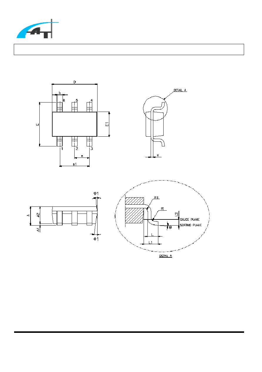
PACKAGE DIMENSION
Advanced Analog Technology, Inc.
≠
≠
≠
Advanced Analog Technology, Inc
.
≠
Page 21 of 24 V 1.0
AAT8660 Series
PACKAGE DIMENSIONS (CONT.)
VARIATION (ALL DIMENSIONS SHOWN IN MILLIMETERS)
SYMBOL MIN TYP MAX
A
------ ------ 1.45
A1
------ ------ 0.15
A2 0.90
1.15
1.30
b 0.30
------
0.50
c 0.08
------
0.22
D 2.90
BSC
E 2.80
BSC
E1 1.60
BSC
e 0.95
BSC
e1 1.90
BSC
L 0.30
0.45
0.60
L1 0.60
REF
L2 0.25
BSC
R 0.10
------ ------
R1 0.10
------
0.25
o
0
o
4
o
8
1
o
5
o
10
o
15
NOTE:
1 JEDEC OUTLINE: MO-178 AB

Advanced Analog Technology, Inc.
≠
≠
≠
Advanced Analog Technology, Inc
.
≠
Page 22 of 24 V 1.0
AAT8660 Series
TAPE AND REEL
PACKING METHOD: 3,000PCS/REEL, 5 REELS/BOX

Advanced Analog Technology, Inc.
≠
≠
≠
Advanced Analog Technology, Inc
.
≠
Page 23 of 24 V 1.0
AAT8660 Series
TAPE AND REEL (CONT.)
X.XXX X
±
0.0025
X.XXX
±
0.006
X.XX
±
0.025
X.X
±
0.10
X
±
0.25
UNIT: MILLIMETERS

Advanced Analog Technology, Inc.
≠
≠
≠
Advanced Analog Technology, Inc
.
≠
Page 24 of 24 V 1.0
AAT8660 Series
PART MARKING
PREVIOUS SOT26 TOP MARKING
AXXX
NOTE: SOT26 HAS NO BACK MARKING.
CURRENT SOT26 TOP MARKING
AXX