
CRYSTAL OSCILLATORS
Rev. B
357 Beloit Street, P.O. Box 457, Burlington, WI 53105-0457 U.S.A. Phone 262/763-3591 FAX 262/763-2881
Email:
nelsales@nelfc.com
www.nelfc.com
Data Sheet 0637B
LVDS TCXO/TCVCXO
AA-XADXXX Series
Description
The AA-XADXXX
Series
of quartz crystal oscillators provide excellent temperature stability with
LVDS complementary outputs. The device is packaged in a miniature, low profile leadless FR4
based package with gold plated pads, which enhances compatibility with PCB material.
Creating a Part Number
AA - X AD X X X -FREQ
Package code
AA � 6 pad 7.5x5x2 SMD
Operating Voltage
A 3.3 V � 5%
B 2.5 V � 5%
Temperature Range, �C
A 0 to 50
B 0 to 70
C -20 to 70
D -40 to 85
9 customer specific
Temperature Stability, ppm
E �1
F �2
G �2.5
9 customer specific
TCXO/TCVCXO Option
X No V. Control
Y w/V. Control
CRYSTAL OSCILLATORS
Rev. B
357 Beloit Street, P.O. Box 457, Burlington, WI 53105-0457 U.S.A. Phone 262/763-3591 FAX 262/763-2881
Email:
nelsales@nelfc.com
www.nelfc.com
Data Sheet 0637B
LVDS TCXO
AA-XADXX Series
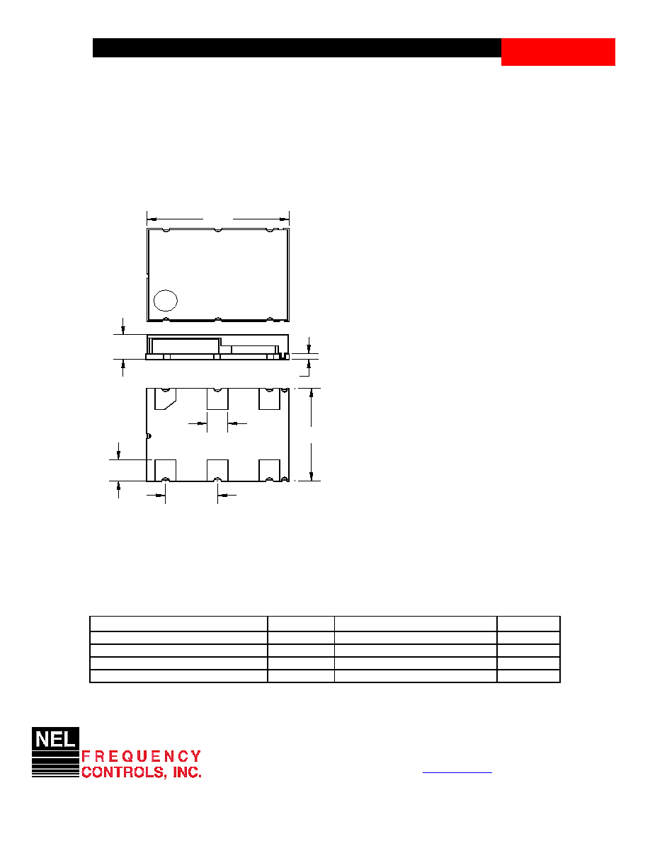
Drawing Specification
0.5
2.0
1
2
3
4
5
6
1.37
1.37
2.540
5.20
7.5
NEL
Absolute Maximum Ratings
Parameter Symbol Value Unit
Operating Temperature Range
To
-40 to +85
�C
Storage Temperature Range
Tst
-50 to +90
�C
Supply Voltage
Vcc
-0.5 to 4.5
V
Voltage Control
Vc
0 to Vcc
V
Pin Connections:
1 � N/C or Vc
2 � N/C
3 � GND
4 � OUT
5 � Complementary OUT
6 � Vcc
Dimensions are typical in mm

CRYSTAL OSCILLATORS
Rev. B
357 Beloit Street, P.O. Box 457, Burlington, WI 53105-0457 U.S.A. Phone 262/763-3591 FAX 262/763-2881
Email:
nelsales@nelfc.com
www.nelfc.com
Data Sheet 0637B
LVDS TCXO
AA-XADXX Series
Electrical Parameters
Parameter Symb Conditions,
Note MIN
TYP MAX Unit
Nominal Frequency
Fo
12.8
120
MHz
Supply Voltage
Vcc
Code A
Code B
3.135
2.375
3.3
2.5
3.465
2.625
V
Supply current
Icc
40
50
mA
Load
At receiving end between
the outputs
90 100 110 Ohm
Vod Differential
amplitude
247 330
454
mV
Amplitude
error
50 mV
Vof Offset
Voltage
1.125 1.25 1.375
V
Output Levels
Offset voltage error
50
mV
Duty Cycle
(Symmetry)
At outputs crossing, room
temperature
45/55 50/50 55/45
%
Rise/Fall Time
Tr/Tf
20 to 80, 80 to 20 %
0.35
0.4
ns
Integrated
J
Integrated from Phase Noise,
12 KHz to 20 MHz , RMS
0.2
ps
Random
period,
2.5
2.5
ps
Jitter
Wavecrest
characterized
Accumul.
pk-to-pk
20
ps
Deterministic
F>40MHz 3 6 ps
Sub-harmonics
<40
M
>40 M
-50
-45
dBc
Phase Noise
�(f)
20 MHz
@ 10 Hz
@100 Hz
@1 KHz
@10KHz
@100KHz
@>1MHz
-85
-115
-135
-140
-145
-148
dBc/Hz
Frequency stability
F/F
Over Temp -30 to 80 C
See
chart
Aging, 1
st
year
Aging 10 years
Load
Vcc
Reflow
Calibration as shipped
2.5
1
3.5
0.1
0.1/V
2
1
ppm
Pullability
(Vc option)
0.3V
to
3.0V
5
ppm

CRYSTAL OSCILLATORS
Rev. B
357 Beloit Street, P.O. Box 457, Burlington, WI 53105-0457 U.S.A. Phone 262/763-3591 FAX 262/763-2881
Email:
nelsales@nelfc.com
www.nelfc.com
Data Sheet 0637B
LVDS TCXO
AA-XADXX Series
Environmental and Mechanical Characteristics
Operating temp.
range
see part # table
Mechanical Shock
Per MIL-STD-202, Method 213, Cond. A
Thermal Shock
Per MIL-STD-883, Method 1011, Cond. A
Vibration
Per MIL-STD-883, Method 2007, Cond. A
Hermetic Seal
Leak rate less than 1x10⁻⁸ atm.cc/s of helium
Soldering conditions
See MAX reflow profile below
MAX Reflow Profile