
2087
ACC Microelectronics Corporation, 2500 Augustine Drive, Santa Clara, CA 95054
Phone: (408) 980-0622 Fax: (408) 980-0626
ACC2087
ENHANCED SUPER CHIP
DATA BOOK
ADVANCED INFORMATION
AUGUST 1996
Revision 1.1

2087
ACC Micro
TM
ACC Microelectronics Corporation, 2500 Augustine Drive, Santa Clara, CA 95054
Phone: (408) 980-0622 Fax: (408) 980-0626
ACC Microelectronics Corporation
2500 Augustine Drive,
Santa Clara, CA 95054
Phone: (408) 980-0622 Fax: (408) 980-0626
Copyright 1996 ACC Microelectronics Corporation. All rights reserved.
P/N 520141
Revision 1.1
August 1996
No part of this document may be copied or reproduced in any form or by any means without the prior written
consent of ACC Microelectronics Corporation.
ACC Microelectronics Corporation makes no warranty for the use of its products and bears no responsibility for
any errors which might be appear in this document. Specifications are subject to change without notice.
ACC Micro is a trademark of ACC Microeletronics Corporation.
IBM, AT, XT, PS/2, Micro Channel are trademarks of International Business Machines.
Pentium, Intel are trademarks of Intel Corporation.
M1 is a trademark of Cyrix Corporation.
K5 is a trademark of Advanced Micro Devices

2087
ACC Micro
TM
i
Table of Contents
Title
Page
1.0
ACC2087 Introduction
1
1.1 ACC2087 Features
1
1.2 ACC2087 System Block Diagram
1
1.3 ACC2087 Internal Block Diagram
3
2.0
ACC2087 Functional Description
4
2.1 CPU Interface
4
2.2 80387 Interface Control
4
2.3 Clock Generator
4
2.4 Clock Mode Selection
5
2.5 Stop Grant, Stop Clock, for 1X Clock Scaling
6
2.6 Clock Throttling
7
2.7 Local Bus Peripheral Support
7
2.8 Intel System Management Mode Interface
8
2.9 Power Management Features
10
2.10 Shadow Register Table Description
11
2.11 High Performance Cache Controller
14
2.12 Memory Controller
15
2.13 Memory Mapping
16
2.14 Shadow RAM
16
2.15 Interrupt Controllers
16
2.16 DMA
16
2.17 Memory Mapper
17
2.18 Timer/Counter
17
2.19 ACC2087 I/O Address Map
17
2.20 PIO
17
2.21 DMA Arbitration Logic
17
2.22 Refresh Generation Logic
17
2.23 Staggered Refresh Logic
18
2.24 NMI and Port B Logic
18
2.25 Bus Controller and Converter
18
2.26 Turbo Speed Control Logic
19
2.27 8-bit/16-bit ROM Options
20
2.28 128K/64K ROM BIOS Range
20
2.29 Reset and Shutdown Logic
20
2.30 OS/2 Optimization
21
2.31 Floppy Disk Drives
22
2.32 Serial Port Interface
38
2.33 Parallel Port Interface
51

2087
ACC Micro
TM
ii
Table of Contents
contd.
Title
Page
3.0
ACC2087 Pin Description
56
3.1 ACC2087 Pin Descriptions
56
3-1 Clock Interface
56
3-2 Reset Interface
56
3-3 CPU Interface
56
3-4 Power Management/Cache/DRAM/AT Multiplex Interface
59
3-5 Dedicated Power Management Interface
60
3-6 Dedicated Cache Interface
61
3-7 DRAM Interface
62
3-8 AT Bus Interface
62
3-9 Keyboard/Mouse Interface
65
3-10 FDC Interface
65
3-11 COM1 Interface
66
3-12 COM2 Interface
66
3-13 IDE and LPT1 Interface
67
3.2 ACC2087 Numerical Pin List
68
3.3 ACC2087 Desktop vs. Notebook Multiplexed Pin Summary
69
3.4 ACC2087 Pins Status for Various CPU Types
69
3.5 ACC2087 Numerical Pin List with Multifunction pins and Power
Plane Description
70
4.0
ACC2087 Register Settings
73
4.1 ACC2087 Register Settings
73
5.0
ACC2087 Upgrade -- Advanced Parallel Port
112
5.1 Description, Features, and Block Diagram
112
5.2 Features
112
5.3 Block Diagram
112
5.4 Programmable Configuration Registers
114
5.5 Parallel Port Interface
115
6.0
ACC2087 DC Specifications
116
7.0
ACC2087 AC Specifications
125
8.0
ACC2087 Package Specifications
150
Appendix A-1 List of Sales Representatives

2087
ACC Micro
TM
1
Section 1
Introduction
1.1
2087 Features
Supports Intel iDX4, AMD AM486, Cyrix 5x86, TI 486s, and IBM Blue Lightning microprocessor with
operation up to 50 MHz
3.3V / 5.0V mixed voltage system design
Level 1 Write Back Cache
Level 2 Cache Controller
- Support either write back or write through implementation
- Up to 2 MB in cache size
High Performance DRAM Controller
- Supports four banks of 32-bit DRAM, Fast Page Mode only, allowing up to 64 MB memory
Integrated Peripheral Controller: 2 x 8237, 2 x 8259, 1 x 8254, 1 x 74612
Integrated Floppy Disk Controller supports two floppy disk drives
Supports one IDE interface
Supports two high speed 16C550 compatible UARTs with 16 Byte FIFOs
Supports one bi-directional Parallel port with ECP mode
Support PPM mode where Floppy Disk Drive can be used on Parallel Port
PS/2 compatible Keyboard Controller and Mouse
Power Management Control
- Power-On Suspend
- Power-Off Suspend
- Doze / Idle Detection
- Suspend / resume Button
- APM support
- SMM / SMI
- Stop Clock Protocol
- Battery monitoring signal and dedicated low-battery warning alarm
Supports Flash EPROM
Local Bus IDE
Fast reset / Fast gate A20 (Port 92)
256-pin PQFP device

2087
ACC Micro
TM
2
1.2
2087 System Block Diagram

2087
ACC Micro
TM
3
1.3
2087 Internal Block Diagram

2087
ACC Micro
TM
4
Section 2
Functional Description
2.1
CPU Interface
The ACC2087 supports the 486 and 386DX CPUs. The CPU interface selection is determined by detecting a
pull up or pull down resistor on pin 172 (M486) during the reset period. A pull up resistor on pin 172 will
trigger the ACC2087 operating in the 486 mode. A pull down resistor on pin 172 will trigger the ACC2087
operating in the 386DX mode.
486DX mode configuration
386 mode configuration
2.2
80387 Interface Control
The 80387 interfaces directly to the 386DX with the error-reporting logic built in the ACC2087. A coprocessor
error is sent to the ACC2087, generating an interrupt request to the CPU, followed by a service request. A
write operation to I/O port 0F0 will clear the interrupt request.
2.3
Clock Generator
The ACC2087 Clock Generator provides flexible clock signals to support internal and external timing
requirements. Clock outputs for the CPU, the NPU, and the Keyboard Controller are generated from these
inputs. Three clock sources (CLKSRC, X24M and X14M) are used to derive the system clock output
(SYSCLK).
Signal X14M interfaces to a 14.318 MHz crystal to generate a 14.318 MHz frequency. A 24 MHz crystal is
used by signal X24M to provide all timing signal for the integrated floppy disk controller. The CLKSRC input
is the same input to the CPU clock. CLKSRC input must be driven by an external oscillator. This input is one
or two times of the CPU operation clock and provides turbo mode operation in 1x or 2x clock mode,
respectively.
The AT Bus clock can be derived from three sources: CLKSRC, X14M, and X24M (by programming register
6h, bit 4-0). CLKSRC can be divided to an approximated 16MHz frequency, or use the 14.318 MHz directly,
or it can be generated from the external 24 MHz directly.

2087
ACC Micro
TM
5
2.4
Clock Mode Selection
The ACC2087 supports both 1x clock and 2x clock. The clock phase is determined by selecting pin 51,
CLKX1 signal for 1x clock from the ACC2087 or by selecting pin 49, CLKX2 signal for 2x clock from the
ACC2087.
The 2x clock has a clock source, which is two times the CPU operation clock. In 2x clock, every cycle consists
of two CLKI periods. 2x clock can be used for both the 486DX/SX systems or 386DX systems. In 486 mode,
the ACC2087 provides a dedicated 486 Clock, which is a half of the CLKSRC . This pin, (pin 49) CLKx2, is
actually the phase 1 reference clock.
2x clock
The 1x clock has a clock source which is one times of the CPU operation clock. In 1x clock, every CLKI input
period becomes one completed cycle. 1x clock is used primarily for the 486 systems. CLKx1 can be used as
486 CPU clock input.
1x clock

2087
ACC Micro
TM
6
2.5
Stop Grant, Stop Clock, for 1X Clock Scaling:
In a Notebook system, the ability to switch CPU clock is a very important feature for power saving. The
ACCACC2087 supports this feature by providing the interface to the CPU for Stop Grant and Stop Clock for
1x Clock Scaling functions.
ACC2087 Clock Scaling
1x Clock Stop-Grant Protocol
2X Clock Mode: When Register 20h bit 5 and Register 8h bit 3-0 of the ACC2087 are set, the "Turbo" pin can
toggle CPU clock between turbo and sleep frequency. The CPU clock can also be switched between turbo and
sleep frequency by programming Register 1Bh bit 0 to toggle the frequency.
1X Clock Mode: When Register 20h bit 3 is set to zero, ACC2087 will toggle between turbo and sleep
frequency.
2087
ACC Micro
TM
7
2.6
Clock Throttling:
To further reduce the power consumption in the Notebook system, the ACC2087 supports another mode called
Clock Throttling. After scaling the CPU clock, the ACC2087 can periodically assert the STPCLK# request
which will force the CPU into Stop Grant State. Hence the CPU power can be further reduced.
2.7
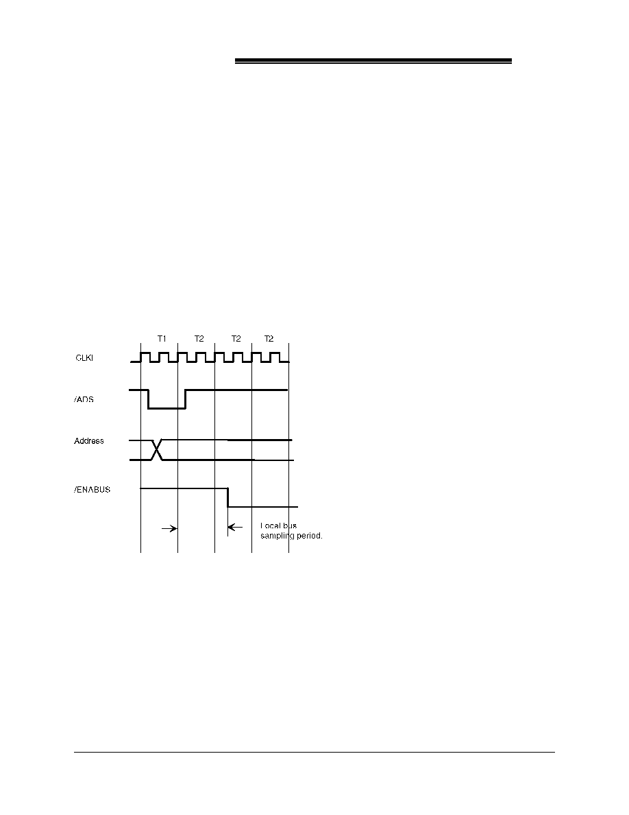
Local Bus Peripheral Support
Master / DMA Mode and SMM Support in Local Bus Cycle
The ACC2087 supports VL-Bus with master and DMA modes. To further enhance the flexibility, the local bus
can be detected under System Management Mode (SMM).
The ACC2087 determines whether the cycle is a local bus cycle or not by detecting the existence of the local
bus cycle signal, signaled by a local bus device. When the ACC2087 Register 1Bh, bit 4, is set to one, pin 127
(READY0#, LBA#) becomes the LBA# pin. This pin is connected to the local bus device's local bus
acknowledge signal. When LBA# is asserted low, the ACC2087 will terminate all the bus cycles, and
relinquish the control to the local bus. The ACC2087 starts to sense the LBA# pin status from the end of T1
until the beginning of the ENABUS# as shown below.
Local Bus Detection

2087
ACC Micro
TM
8
For local bus devices operating with a fast speed CPU clock, the ACC2087 offers an option to delay the ADS#
one cycle internally to detect the local bus acknowledge or delay the AT bus for one cycle as shown below.
Register 1Ah, bit 7, programs the ACC2087 internal ADS# timing. Register 18h, bit 6, programs the AT bus
cycle delay.
Local Bus Delay Option
2.8
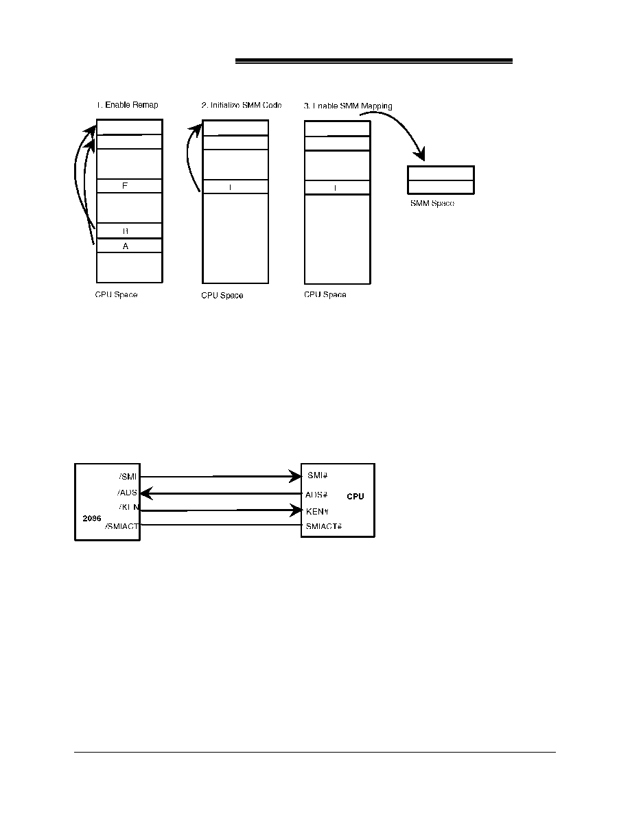
Intel System Management Mode Interface (SMM)
System Management Mode (SMM) is designed to handle power management interrupts that are totally
transparent to the existing programs, operating systems and CPU operation modes. The ACC2087 contains
dedicated logic to interface with SMM implemented by the Intel SL-enhanced 486 for battery-powered portable
computers. The ACC2087 utilizes the DRAMs located between segments A000h and B000h as the separate
SMM memory (SMRAM) required by SMM functions.
Before activating the SMM function, the system BIOS first needs to load the SMM service routine into the
separate SMM memory (SMRAM). During power-up, the system BIOS can turn on the ACC2087 remap
feature so that memory physically located between segment A000h to segment B000h can be accessed logically
through locations between X + 128K and X if X memory is installed in the system. The system BIOS then
loads the SMM code into this area, disables the remap and then enables ACC2087 SMM support. The remap
space is now reserved for SMM. Two 64K blocks are available and one can be programmed as segment 3000h
for executing the SMI handler. The remap function will not be available when SMM is used.
2087
ACC Micro
TM
9
SM-RAM Mapping and Initializing for System Management Mode
The power management interrupt generated by the ACC2087 is connected to the CPU SMI# pin. The SMM
interface circuit has been integrated in the ACC2087 to handle SMM cycle, memory map, and CPU internal
cache.
The ACC2087 will enter SMM cycles when it detects SMIACT# being asserted low by the CPU. The physical
memory (30000h - 3FFFFh) dedicated to System Management Mode (SMM) will be enabled. CPU will use
this dedicated SMRAM to perform SMM state save and state restore starting at address location 3FFFFh,
proceeding downward in a stack-like fashion and execute the SMI handler starting at address location 38000h.
Register 1Fh in the ACC2087 contains the SMI enable bits. Setting bit 4 to one will enable the SMM . While
bit 5 provides the access to the SMRAM starting at segment 3000h.
System Management Mode Interface (Intel SL-Enhanced CPU)

2087
ACC Micro
TM
10
2.9
Power Management Features
The ACC2087 provides a powerful mechanism of system power management that is completely transparent to
the operating system and application software. It was designed from the system level to synthesize and manage
power consumption for the lowest power operation while maintaining system performance in the portable
system.
The ACC2087 implements four special power saving modes to provide the most sophisticated system
information needed for power management application. They are "Local Standby" , "Global Standby" ,
"Suspend / Resume" , and "Doze" mode. The ACC2087 also provides a dedicated battery low input pin
(LBAT#) and warning timer for an external battery pack. A transition on LBAT# should trigger this
programmed warning timer. A 1khz tone will be generated through the speaker output as soon as the LBAT#
transition is detected. If no transition has been detected, upon warning timer time-out, an SMI will be
generated.
Local Standby Mode (LSM)
The "Local Standby" mode provides three dedicated local standby control circuits to monitor activity on HDD ,
I/O address for general chip select (GCS), and VRAM, Keyboard/Mouse, respectively. When the associated
programmed timer is timed out, an optional SMI will be generated and status bit will be set. Any break event
such as hard disk access will generate SMI and bring system back to normal operation.
Global Standby Mode (GSM)
When the system has been idle for a programmed standby timer count , and there is
no screen activity for a programmed VRAM count, the system can go into global standby mode. All of the
peripheral devices can be powered off and the CPU clock can be stopped under global standby mode.
Suspend and Resume Mode
The suspend mode can be entered by pressing the suspend/resume button or receiving a low battery input. In
addition to the suspend / resume button, the ACC2087 has two user-defined buttons, User button and Standby
button, which can bring the system to suspend mode.
The suspend to disk and resume feature is also supported by the ACC2087 through the SL-compatible shadow
register.
Doze Mode
Doze mode provides a mechanism that allows power saving even between the keystrokes. This mechanism
utilizes the Frequency Modulation (FM) and Pulse Modulation (PM) techniques which are commonly used in
the
telecommunications field. This mode is used not only to provide the temperature control when CPU is busy
(non-Doze) but also to further reduce power consumption when CPU is not busy (Doze).

2087
ACC Micro
TM
11
Architecture of System and Power Management
2.10
Shadow Register Table Description
All defined register bits in the ACC2087 are readable and writeable to support the Intel SL type of shadow
register. Also the F2 register is now readable to further support the power-saving feature.
Through the shadow registers, the ACC2087 can be powered off and its current state can be suspended to the
disk. The device then can be powered back on to the same state as before the last power off when it is desired.
This suspend and resume capability minimizes the system's battery power consumption.
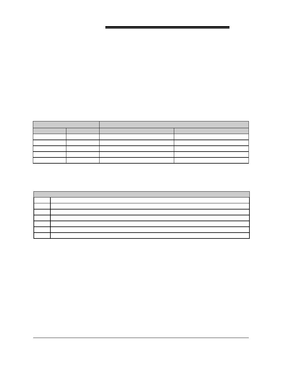
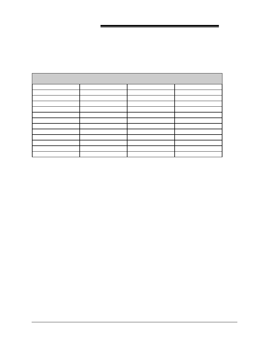
Table 1.0 summarizes all of the shadow registers and their descriptions.
1.
All the registers listed are originally write-only in ISA standard. The shadow mechanism makes them
readable through the 0F2h/0F3h indexing scheme.
2.
For some DMA registers that contain 2 bytes but have only one index assigned, the following
sequence
must be followed:
cli
;make sure the sequence will not be broken
out 0f2h, indx
;output index, clear the byte pointer, point to low byte
mov ah, al
;save it somewhere
in al, of3h
;high byte, byte pointer will not be changed, stay at high byte.

2087
ACC Micro
TM
12
*
Any write to 0F2h with index 0Axh will clear the byte pointer, which will set pointer
to low byte. The first read from 0F3h after writing the index will set the pointer to
high byte.
*
Only one byte pointer is shared by all paired register sets.
*
The first read from 0F3h will return the low byte, the second read will return the high byte.
3.
For those registers that do not use all the bits, unused bits status are undefined. Software needs to
mask out these bits when it restores.
4.
For DMA base address registers, word count registers, channel mode registers, and channel mask
registers, the value read back from the shadow registers are the original values loaded.
5.
The value read back from shadow registers for the timer count are the original values loaded.

2087
ACC Micro
TM
13
Shadow Register Table
Register Name
SL Mnemonic
Original
Address
Index
Comment
DMA CH0 Base Address
SHDMA0BA
00H
0A0H
2 bytes
DMA CH0 Count
SHDMA0WC
01h
0A1h
2 bytes
DMA CH1 Base Address
SHDMA1BA
02h
0A2h
2 bytes
DMA CH1 Count
SHDMA1WC
03h
0A3h
2 bytes
DMA CH2 Base Address
SHDMA2BA
04h
0A4h
2 bytes
DMA CH2 Count
SHDMA2WC
05h
0A5h
2 bytes
DMA CH3 Base Address
SHDMA3BA
06h
0A6h
2 bytes
DMA CH3 Count
SHDMA3WC
07h
0A7h
2 bytes
DMA CH0 Mode
SHDMA0MOD
0Bh
0C0h
1 byte
DMA CH1 Mode
SHDMA1MOD
0Bh
0C1h
1 byte
DMA CH2 Mode
SHDMA2MOD
0Bh
0C2h
1 byte
DMA CH3 Mode
SHDMA3MOD
0Bh
0C3h
1 byte
DMA CNTLR 1 Mask Reg.
SHDMAMSK1
0Fh
0C4h
1byte
PIC1 ICW2
SHINT1ICW2
21h
0D0h
1 byte
PIC1 ICW4
SHINT1ICW4
21h
0D1h
1 byte
PIC1 OCW3
SHINT1OCW3
20h
0D2h
1 byte
NMI Mask & RTC index
SHNMIMASK
70h
0D6h
1 byte
TMR 1 CNTR 0 cnt low
SHT1CH0CL
40h
0CAh
1byte
TMR 1 CNTR 0 cnt high
SHT1CH0CH
40h
0CBh
1 byte
TMR 1 CNTR 1 cnt low
SHT1CH1CL
41h
0CCh
1 byte
TMR 1 CNTR 1 cnt high
SHT1CH1CH
41h
0CDh
1 byte
TMR 1 CNTR 2 cnt low
SHT1CH2CL
42h
0CEh
1 byte
TMR 1 CNTR 2 cnt high
SHT1CH2CH
42h
0CFh
1 byte
DMA CH4 Base Address
SHDMA4BA
0C0h
0A8h
2 bytes
DMA CH4 Count
SHDMA4WC
0C2h
0A9h
2 bytes
DMA CH5 Base Address
SHDMA5BA
0C4h
0AAh
2 bytes
DMA CH5 Count
SHDMA5WC
0C6h
0ABh
2 bytes
DMA CH6 Base Address
SHDMA6BA
0C8h
0ACh
2 bytes
DMA CH6 Count
SHDMA6WC
0CAh
0ADh
2 bytes
DMA CH7 Base Address
SHDMA7BA
0CCh
0AEh
2 bytes
DMA CH7 Count
SHDMA7WC
0CEh
0AFh
2 bytes
DMA CH4 Mode
SHDMA4MOD
0D6h
0C5h
1 byte
DMA CH5 Mode
SHDMA5MOD
0D6h
0C6h
1 byte
DMA CH6 Mode
SHDMA6MOD
0D6h
0C7h
1 byte
DMA CH7 Mode
SHDMA7MOD
0D6h
0C8h
1 byte
DMA CNTLR 2 Mask Reg.
SHDMAMSK2
0DEh
0C9h
1 byte
PIC2 ICW2
SHINT2ICW2
0A1h
0D3h
1 byte
PIC2 ICW4
SHINT2ICW4
0A1h
0D4h
1 byte
PIC2 OCW3
SHINT2OCW3
0A0h
0D5h
1 byte

2087
ACC Micro
TM
14
2.11
High Performance Cache Controller
The integrated ACC2087 cache controller supports a direct mapped cache from 32 Kbytes up to 2 Mbytes in
size. The direct mapped architecture means that a specified line in the cache is capable of caching only a
certain range of memory addresses. The low order address bits choose the location (index) while the high order
address bits (tag) identify the entry.
As for write policy, the ACC2087 supports either write through or write back cache implementations. In
addition, the ACC2087 cache architecture can be used in both 386DX and 486 applications. For a 386DX
design, the ACC2087 cache controller can be used to support a primary cache. In a 486 AT system, if the
internal cache of the 486 is enabled, the ACC2087 direct mapped cache can be used as secondary cache.
Write Back Cache Policy
The write back cache policy implemented in the ACC2087 allows the system to minimize the frequency of
unnecessary slow DRAM updates. For instance, when there are consecutive write hit cycles, the ACC2087
simply updates the cache without introducing any memory delay.
A write back cache design allows the write hit cycles to be completed in zero wait state accesses without
updating the system main memory. Therefore, "stale" data is created where cache data and main memory data
are not coherent. A write back cache design uses a "dirty" bit to keep track of whether each cache data line is a
"clean" or "dirty" line. A "clean" line, dirty bit = 0, means the cache data and the corresponding main memory
are identical. A "dirty" line, dirty bit = 1, indicates the cache data has been modified, which at some point must
be written back to main memory.
Following is the write back cache mechanism for ACC2087:
Write Hit
In a cache write hit cycle, the ACC2087 will write to cache and set the "dirty" bit to 1.
Write Miss
In a cache write miss cycle, the ACC2087 will write to DRAM directly.
Read Hit
In a cache read hit cycle, the ACC2087 will read from cache directly.
Read Miss
In a cache read miss cycle, the ACC2087 will examine the "dirty" bit status. If it is non-dirty, cache
will be updated directly. If it is dirty, cache data will be "write back" before being updated.
The ACC2087 write back cache is enabled by programming configuration register 1E. When bit 3 in Register
1Eh is set to 1, write back is enabled and the ACC2087 will use integrated comparators for determining cache
hit or miss status.
As described earlier, "dirty" status must be updated as well as detected for write back mode. MA10 becomes
the dirty bit status signal (DIRTY) and NA# becomes the dirty bit write enable signal (DTYWE#). Refer to
figure 1.4.
2087
ACC Micro
TM
15
Posted Write and Write Through
The ACC2087 cache controller supports write-through and post write cache update options to prevent old data
from being used.
The write-through option is the simplest way to keep cache coherent. In a cache write hit cycle, the memory
controller will update the DRAM at the same time that it is written to the cache. The ACC2087 cache controller
default mode is write-through mode.
Write Back Cache Circuit Block Diagram
The ACC2087 also supports posted write cache system by programming Configuration Register 4h, bit 7=1.
The posted write option allows the data to be buffered before updating to the main memory. The system
performance is therefore increased, since the processor can start a new cycle before the write cycle to the main
memory is completed.
Cache Burst and Line Size
The ACC2087 supports a flexible line size structure and cache burst. The ACC2087 supports 32 bit, 64 bit, or
128 bit line sizes. Configuration Register 4h, bits 2 and 1 determine the line size. In the case of a cache read
hit cycle, the ACC2087 will pull the burst ready signal, BRDY#, low and fill the 486 internal cache lines
quickly. A 128 bit line size requires only 5 cycles to fill the cache lines. A 64 bit line size requires 3 cycles.
In the case of a read miss cycle, the ACC2087 burst mode will generate four continuous DRAM read cycles for
a 128 bit line size to fill both 486 internal and external cache. For a 64 bit line size, the ACC2087 burst mode
will generate two burst cycles instead of four.
2.12
Memory Controller
The Memory Controller is a key feature of the ACC2087. This versatile circuit provides complete control of up
to 64 megabytes of system DRAM. In any control mode, it generates up to four Row Address Strobes
(RAS#0-3) and one Memory Write Enable signal (WEN#). The Memory Controller also provides the interface
to transfer control to a DMA controller or an AT Bus master.
The ACC2087 Memory Controller supports 256KB, 512KB, 1MB and 4MB DRAM devices. The ACC2087
provides all control signals and programmable control to support 256Kx1, 512Kx1, 1Mx1, 1Mx4, 4Mx1 and
4Mx4 (symmetrical only).

2087
ACC Micro
TM
16
2.13
Memory Mapping
Memory Mapping translates system RAM within the 640 KB to 1MB range, which is reserved for the system
ROM and BIOS application, to an accessible address range above the physical RAM space. For example, if 4
MB of memory are installed, and the memory mapping feature is on, the DRAMs in the 640 KB to 1MB range
are mapped to an address immediately above 4 MB.
Memory Mapping is enabled by bit 7 of Register 0h in the configuration registers. When Shadow RAM is
enabled simultaneously with Memory Mapping, the quantity of RAM available for Memory Mapping is
reduced. If Shadow RAM segment F is enabled, 320KB of RAM can be mapped. If Shadow segment E is
enabled, 256KB of RAM can be mapped. If any of the segments C0, C1, or D is enabled, 128 KB of RAM can
be mapped. This mapping function can be used in all memory options, except option 24.
2.14
Shadow RAM
Shadow RAM provides an option to transfer BIOS or video-extension BIOS program codes into system RAM.
This option provides significant performance improvement for applications requiring intensive BIOS calls.
Shadow RAM implements an alternate BIOS source by copying the complete EPROM program code into
system RAM. This is referred to as "shadowing" because the DRAM and EPROM are both located in the same
physical address space. This change is transparent to the rest of the system. ROM can then be disabled,
allowing the RAM to respond in its place.
The ACC2087 Shadow RAM is configured in five independent segments: 00C0000 to 00C7FFF (Shadow C0),
00C8000 to 00CFFFF (Shadow C1), 00D0000 to 00DFFFF (Shadow D), 00E0000 to 00EFFFF (Shadow E),
and 00F0000 to 00FFFFF (Shadow F). Each segment can be enabled for shadow operation individually or
simultaneously.
Enabling a Shadow RAM segment requires two steps. The "shadow enable" configuration bit for the segment
to be shadowed must be set to allow the transfer of code from EPROM to DRAM. The second step sets the
"Shadow Read Only" configuration bit of the corresponding segment to protect the Shadow RAM.
Interrupt Controllers
2.15
Interrupt Controllers
There are two programmable interrupt controllers for the ACC2087. They are fully compatible with Intel's
8259 controller, providing up to 15 interrupt sources
(14 external and 1 internal). The internal line connects to the 8254 Counter 0 output.
These interrupt controllers prioritize interrupt requests to the CPU.
2.16
DMA
The ACC2087 has two DMA controllers, compatible with the Intel 8237, which provide a total of seven
external DMA channels.
Combined with the Memory Mapper, each DMA channel has a 24-bit address output to access data throughout
the 64 megabyte system address space.

2087
ACC Micro
TM
17
2.17
Memory Mapper
The ACC2087 has a built-in logic equivalent to the 74LS612, generating the upper address bits during a DMA
cycle.
2.18
Timer/Counter
The ACC2087 provides three internal counters, which are compatible with the 8254. The clock input for each
counter is tied to a clock of 1.19 MHz, which is derived by dividing the
14.318 MHz crystal input by 12. The output of Counter 0 is connected to the IRQ0 input of interrupt controller
1. Counter 1 initiates a refresh cycle and Counter 2 generates sound waveforms for the speaker.
2.19
ACC2087 I/O Address Map
The ACC2087 I/O address decode is fully compatible to the IBM PC/AT requirements. The ACC2087 has
decoded the I/O address range from 000 to 0FF to allow users to use the I/O areas not used by the IBM PC/AT.
Hex Range
Device
000-00F
DMA controller 1, 8237A-5
020-021
Interrupt controller 1, 8259A, Master
040-043
Timer, 8254
060/064
Integrated Keyboard Controller
060-064
External Keyboard Controller
070-071
Real-time clock, NMI (non-maskable interrupt) mask
080-08F
DMA page register, 74LS612
092
Alternative Gate A20 and FAST RESET Register.
0A0-0A1
Interrupt controller 2, 8259A
0C0-0DF
DMA controller 2, 8237A-5
0F0
Clear Math Coprocessor Busy
0F1
Reset Math Coprocessor
0F2
ACC2087 Configuration Register Index
0F3
ACC2087 Configuration Register Data
0F8-0FF
Math Coprocessor
2.20
PIO
The PIO is the system configuration to control the speaker port. It also has circuitry to detect refresh. This
condition can be read back as Bit 4 of I/O Port 61h.
2.21
DMA Arbitration Logic
There are two possible sources for a hold request to the CPU. Either the DMA controller issues a hold request
or the output of Counter 1 in the 8254 makes a low to high transition. The HOLD line is active when either
source is requesting a hold. The ACC2087 contains the logic to do the arbitration.
2.22
Refresh Generation Logic
The ACC2087 contains circuitry to perform DRAM refresh cycle. Refresh circuitry contains an 8-bit counter
for address SA0-7 during a refresh. In addition, three more address counter bits are presented inside the
ACC2087 to support refresh for DRAMs up to 4M bits.

2087
ACC Micro
TM
18
2.23
Staggered Refresh Logic
The ACC2087 refresh logic works to perform a periodic refresh for both system DRAM and extended RAM on
the AT Bus. The ACC2087 initiates a refresh cycle by driving its REFRESH# output low, and driving the
refresh address onto the MA Bus, simultaneously generating staggered refresh pulses on the four RAS outputs.
The RAS outputs are staggered to reduce the current drain caused by the refresh operation. During each refresh
cycle, the ACC2087 drives the current refresh address onto the AT address bus. This provides the refresh
address for extended memory.
2.24
NMI and Port B Logic
The ACC2087 contains non-maskable interrupt (NMI) signal generation logic. An NMI can be caused by an
I/O error or by a parity error. Port B identifies the source of the error. At power up, the NMI signal is masked
off. NMI is enabled by writing to I/O address 070 with bit 7 low; NMI is disabled by writing to I/O address
070 with bit 7 high.
2.25
Bus Controller and Converter
The flexible ACC2087 Bus Controller provides all of the control logic needed to interface to the CPU, alternate
masters, local memory, primary or secondary cache and the AT bus. Each access may be initiated by the
ACC2087 decoding the address and cycle type provided on the local CPU bus. The cycle type is determined
by monitoring the signals D/-C, W/-R and M/-IO.
The bus controller has seven modes of operation which are defined as follows:
Local Memory Mode
Local memory mode is entered if the CPU addresses are part of the installed memory and the cycle is defined as
a memory access.
Local Peripheral Mode
Local Peripheral Mode is entered when the ACC2087 LBA# signal is asserted during the local bus cycle. The
ACC2087 will ignore all transactions when LBA# is properly asserted. The local bus peripheral decodes the
local address for accesses to the local bus device. The peripheral will assert LBA# and properly complete the
cycle. When the local peripheral bus interface is enabled, READY# is not available for coprocessors. The
Weitek device should be treated as a local peripheral device. The 387 accesses will always include one wait
state.
AT CPU Mode
This mode is active when HLDA is low. The CPU bus controller generates IOR#, IOW#, INTA#, MEMR#,
and MEMW# signals.
DMA Mode
DMA mode is active if HLDA and AEN are active. The DMA controller drives the IOR#, IOW#, MEMR#,
and MEMW# signals.

2087
ACC Micro
TM
19
Refresh Mode
Refresh mode is active when HLDA and REFRESH# are active. MEMR# becomes active at this time to
perform a refresh on both AT bus and local DRAM.
Master Mode
Master mode is active when HLDA is active and a card in the AT slot pulls MASTER# low. The card controls
system address, data line and control line.
Bus Conversion Mode
The ACC2087 contains logic to convert between 16-bit and 8-bit data accessing. During a bus conversion
cycle, the AT bus command strobe (MEMR#, MEMW#, IOR#, or IOW#) is activated two times.
2.26
Turbo Speed Control Logic
The CPU clock frequency can be switched between CLKSRC and the AT clock. The frequency switch can be
generated through either hardware or software. A TURBO pin is provided to support a front panel turbo speed
switch. TURBO high selects CLKSRC as the CPU clock. TURBO low selects AT Bus clock as the CPU
clock.
For power conservation, a standby mode clock control is provided. A system needs to pre-select the standby
frequency first, then BIOS will monitor the activity of the system. If all pre-defined conditions of the standby
mode are satisfied, the system will go into the standby mode by programming bit 3 of Register 8h to 1 or if the
Turbo/Sleep bit has been set to 1. The Turbo pin, when driven low, will force the system into sleep mode.
The standby mode CPU operating frequency can be pre-set by programming bits 2-0 of configuration Register
8h. If AT Bus clock source is at 16 MHz, the standby frequencies output of CLKOUT are set as follows:
Bit 2
Bit 1
Bit 0
Frequency
0
0
0
16 MHz
1
0
0
9 MHz
1
0
1
4 MHz
1
1
0
2 MHz
1
1
1
1 MHz
2087
ACC Micro
TM
20
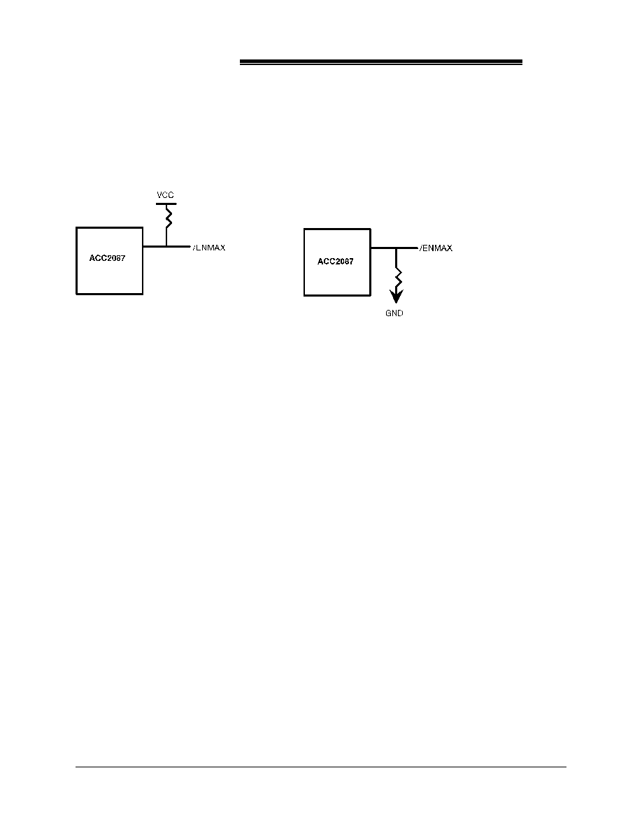
2.27
8-bit/16-bit ROM Options
The ACC2087 supports both 8-bit and 16-bit ROM data buses. It is configured by a pull-up or a pull-down
resistor on pin 139, ENMAX#, as demonstrated below:
8-bit ROM configuration
16-bit ROM configuration
2.28
128K/64K ROM BIOS Range
The ROM BIOS range can be set to two different sizes 64K or 128K to accommodate various application
requirements. Refer to Configuration Register 0h definition to configure the size of the ROM BIOS range.
2.29
Reset and Shutdown Logic
The reset and shutdown logic contains the circuitry for the RESET and CPURDY# signals. Reset circuitry
generates two resets. One is for the general system reset with power on and the other is for the CPU.
The PWRGOOD signal generates a system reset and is synchronized to CPUCLK. When the SWRESET#
signal is generated from the integrated/external keyboard controller (called a warm reset), CPURST is activated
to reset the CPU. CPURST is asserted for at least sixteen CPUCLK cycles and then deactivated for proper CPU
operation.

2087
ACC Micro
TM
21
2.30
OS/2 Optimization
The ACC2087 implements OS/2 optimization, which is a more efficient way to switch back and forth between
real and protected modes in an OS/2 environment when frequent DOS calls are made. Conventional methods
require the processor to communicate with the integrated /external keyboard controller in switching to protected
mode and activating gate A20.
With OS/2 optimization, the ACC2087 allows control of software CPU reset and A20 gating through Port 92h.
Configuration Register Port 92h, Fast A20 Gate, and Alternative RESET Control
Bit
Function
7-2
Reserved
1
Fast Gate A20
0
Fast reset
Bit 1
This bit controls CPU address bit A20. When set to 1, it enables A20. When set to 0, this bit makes
the A20 Signal inactive, thus preventing the Address bus from going beyond the 0FFFFFh boundary in
Real Mode. It is much faster than Gate A20 signal because it is just a simple I/O write operation.
Default is 0.
Bit 0
By setting this bit to 1, application software can reinitialize the microprocessor and switch the
operation from Protected Mode to Real Mode. Setting this bit does not reset the whole system, it only
affects the CPU. This reset function is the same as that of the integrated/external keyboard controller's
"KBRST" signal. However, it provides a faster reset sequence. This bit can be read by application
software to determine if it is a hot rest or cold boot. It can only be set to 0 by writing a 0 to bit 0 of the
register or by power up. Default is 0.

2087
ACC Micro
TM
22
2.31 Floppy Disk Drives
With the ACC2087, designers can build an IBM PC/XT or AT compatible Floppy Disk Drive with fast access
time, high reliability and low cost per bit capability. The ACC2087 integrates the functions of a standard
floppy disk drive controller.
Data separator
Write precompensation circuit
Decode logic
Data rate selection
Clock generation
Drive interface drivers and receivers.
This integration greatly reduces the number of components required to interface floppy disk drives to a
microprocessor system.
The ACC2087 supports up to two floppy disk drives. It is compatible with IBM System 34 double density
format (MFM), and Sony EMCA format.
The ACC2087 contains the decode logic for the internal registers, the write logic and the read logic. The
system address decoder is compatible with the IBM PC drive system. Handshaking signals are provided to
make DMA operation easy to incorporate with the aid of an external DMA control chip. The ACC2087
operates in either DMA or Non-DMA modes. In the Non-DMA mode, the ACC2087 generates interrupts to the
processor each time a data byte is made available. In DMA mode, the processor only needs to load the
command into the ACC2087 which will control all data transfers.
The Data Separator in the ACC2087 minimizes read error rates for high performance floppy disk drives. The
on-chip phase locked loop digital circuit adjusts the clock used during data read to keep it in phase with the data
signal. Write pre compensation is included in addition to the formatting, encoding/decoding, stepper motor
control, and status sensing functions. All inputs are TTL compatible, and outputs are high current, open drain
with direct drive interface.
Using a single 24 MHz crystal input, the ACC2087's internal Clock Generation circuit provides all timing
signals for the sampling clock, write clock, and master clock. It generates 8 and 4 MHz to handle standard data
rates of 500 and 250 Kb/s and 4.8 MHz to support a 300 Kb/s data rate.
The ACC2087 executes the following fifteen commands from the microprocessor.
Read Data
Read Deleted Data
Read a Track
Read ID
Write Data
Write Deleted Data
Format a Track
Scan Equal
2087
ACC Micro
TM
23
Scan Low or Equal
Scan High or Equal
Recalibrate
Sense Interrupt Status
Specify
Sense Drive Status
Seek
FDC Register Descriptions
There are six floppy disk controller registers in the ACC2087, three registers for the status of signals used in
diskette operations, one for data register, and two controller registers. The I/O addresses of these registers are
described in the tables below.
Address
Registers
Primary
Secondary
READ
WRITE
3F0
370
Input Register
3F2
372
Digital output register
3F4
374
Main status register
3F5
375
Data register
Data register
3F7
377
Digital input register
Diskette control register
Input Register (HEX 3F0) (R)
The Input Register is a general purpose input register.
Bit
Function
7-6
0
5
General purpose programmable bit 5.
4
General purpose programmable bit 4.
3
General purpose programmable bit 3.
2
General purpose programmable bit 2.
1
General purpose programmable bit 1.
0
General purpose programmable bit 0.
2087
ACC Micro
TM
24
Digital Output Register . (HEX 3F2) (8-bits) (W).
The Digital Output Register controls drive motors, drive selection, and feature enable. All bits are cleared by
the I/O reset line.
Bit
Function
7-6
Reserved.
5
Motor Enable 1.
4
Motor Enable 0.
3
DMA and Interrupt Enable.
2
Floppy Disk Controller reset.
1,0
Drive Select 0,1
b1 b0
0 0 Select drive 0.
0 1 Select drive 1.
1 0 Reserved.
1 1 Reserved.
Main Status Register (HEX 3F4) (R)
The main status register controls data flow between the microprocessor and the controller.
Bit
Function
7
Request for Master. = 1 Data Register ready for transfer.
6
Data Input/Output. = 1 Data transfer from controller; = 0 Data transfer from the SD bus.
5
Execution Mode (Non-DMA mode). =1 Execution
4
Controller Busy.
= 1 Controller busy.
3
Drive 3 Busy. = 1 Diskette 3 in seek mode. Drive 3 busy.
2
Drive 2 Busy. = 1 Diskette 2 in seek mode. Drive 2 Busy.
1
Drive 1 Busy. = 1 Diskette 1 in seek mode. Drive 1 Busy.
0
Drive 0 Busy. = 1 Diskette 0 in seek mode. Drive 0 Busy.
Data Register (HEX 3F5) (R/W)
The Data Register consists of four status registers in a stack. Only one register is presented to the data bus at a
time. It stores data, commands and parameters, and provides diskette/drive status information. Data bytes are
passed through the data register to program or obtain results after a command.

2087
ACC Micro
TM
25
Status Register 0 (ST0)
Bit
Function
7-6
IC
(Interrupt Code).
7 6
0 0 Normal termination of command.
0 1
Abnormal termination of command.
1 0 Invalid command issue.
1 1 Abnormal termination because the ready signal from FDD changed state during
command
execution.
5
SE, (seek end). = 1 Seek end.
4
EC (Equipment Check). = 1 When a fault signal is received from the FDD, or the track 0 signals
fails to occur after 77 step pulses; = 0 No error.
3
NR (Not Ready). = 1 Drive is not ready; = 0 Drive is ready.
2
HD (Head address). = 1 Head 1 select; = 0 Head 2 select.
1-0
US1,US0 (Unit select).
1 0
0 0 Drive 0 select.
0 1 Drive 1 select.
1 0 Drive 2 select.
1 1 Drive 3 select.
Status Register 1 (ST1)
Bit
Function
7
EN
(End of Cylinder). = 1 When the FDC tries to access a sector beyond the final sector of a
cylinder.
6
Not used. This bit is always 0.
5
DE
(Data Error). = 1 When the FDC detects a CRC error in either the ID field or data field.
4
OR
(Over Run). = 1 If the FDC is not serviced by the host system during data transfer within a
certain time interval.
3
Not used. This bit is always 0.
2
ND
(No Data). = 1 During execution of Read, Write or Verify Data if the specified sector cannot be
found.
1
NW
(Not Writable). = 1 Set if the "write Protect" signal is detected from the diskette drive during
the execution.
0
Missing Address Mark. = 1 When the FDC cannot detect the data address mark or deleted data
address mark.
2087
ACC Micro
TM
26
Status Register 2 (ST2)
Bit
Function
7
Not used. Always = 0.
6
CM (Control Mark). = 1 If deleted data is encountered during execution of the Read Data or Scan
command.
5
DD (Data Error in Data Field). = 1 If the FDC detects a CRC error in the data field.
4
WC (Wrong Cylinder). = 1 Wrong cylinder.
3
SH (Scan Equal Hit). = 1 During execution of the Scan command, if the condition "equal" is
satisfied.
2
SN (Scan Not Satisfy). = 1 During execution of the Scan command, if the FDC cannot find a sector.
1
BC (Bad Cylinder). = 1 Bad cylinder.
0
MD (Missing Address mark in Data Field). = 1 When data is read from the medium, if the FDC
cannot find a data address mark or deleted data address mark.
Status Register 3 (ST3)
Bit
Function
7
FT, Fault.
6
WP, Write Protected.
5
RY, Ready.
4
T0, Track 0.
3
TS, Two-Side.
2
HD, Head Address.
1
US1, Unit Select 1.
0
US0, Unit Select 0.
Digital Input Register (HEX 3F7) (R)
The Digital Input Register is for diagnostic purposes.
Bit
Function
7
Diskette Change (DSKCHG)
6-0
Tri-State

2087
ACC Micro
TM
27
Diskette Control Register (HEX 3F7) (W)
The Diskette Control Register sets the precompensation.
Bit
Function
7-2
Reserved
1-0
Transfer Rates Select and Reduced Write Current Control
00 500Kb/s RWC#=1
01 300Kb/s RWC#=0
10 250Kb/s RWC#=0
11 Reserved RWC#=0
Commands
The diskette controller in ACC2087 is capable of performing fifteen commands. Each command is initiated by
a multi-byte transfer from the microprocessor. The result can also be a multi-byte transfer back to the
microprocessor. Each command consists of three phases: Command, Execution, and Result.
Command
The microprocessor issues all required information to the controller to perform a specific operation.
Execution
The controller performs the specified operation.
Result
After completing the operation, status information and other housekeeping information are made available to
the microprocessor.
Command Symbol Descriptions
A0
Address Line 0. A0 controls the selection of main status register (A0=0) or data register (A0=1).
C
Cylinder Number. Current or selected cylinder (track), numbers 0 through 76.
D
Data. Data pattern to be written into a sector.
D7 -D0 Data Bus. 8 bit data bus, where D7 stand for the most significant bit, and D0 stands for the least
significant bit.
DTL
Data Length. The value of this byte is normally ignored by the controller. However a byte must be
written at this location.
EOT End of Track. The final sector number on a cylinder.

2087
ACC Micro
TM
28
GPL
Gap Length. The length of gap 3. During Read/Write commands this value determines the number of
bytes that VCO sync keeps low after two CRC bytes. During Format command it determines the size
of
gap 3.
H
Head Address. Head number 0 or 1, as specified in the ID field.
HD
Head. Selected head number 0 or 1. (H=HD in all commands)
HLT
Head Load Time. The head load time in the selected FDD (2 to 254 ms in 2 ms increments.)
HUT
Head Unload Time. Time after a Read or Write operation. (16 to 240 ms in 16 ms increments).
MF
Must be 1 to select MFM mode.
MT
Multitrack. If MT is high, a multitrack operation is performed. If MT=1 after finishing a read/write
operation on side 0, FDC automatically starts searching for sector 1 on side 1.
N
Number. The number of data bytes written in a sector.
NCN
New Cylinder Number. New cylinder number reached as a result of the seek operation; desired
position of
head.
ND
Non-DMA Mode.
PCN
Present Cylinder Number. Cylinder number at the completion of the Sense Interrupt Status command,
current position of the head.
R
Record. The sector number to be read or written.
R/W
Read/Write. Either a Read or Write signal.
SC
Sector. Number of sectors per cylinder.
SK
Skip. Skip deleted data address mark.
SRT
Stepping Rate. These bits indicate the stepping rate for the FDD (1 to 16 ms in 1 ms increments).
Stepping rate applies to all drives (FH=1ms, EH=2 ms, etc.).
ST0-ST3
Status 0-Status 3. One of the four registers that store status information after a command has been
executed. This information is available during the result phase after command execution. These
registers must not be confused with the main status register (selected by A0=0). ST0-ST3 are read
only after a command has been executed and only if they contains information relevant to the
command.
STP
Scan Test. If STP=1 during a scan operation, the data in contiguous sectors is compared byte by byte
with data sent from the processor (or DMA). If STP=2, alternate sectors are read and compared.
US0-1 Unit Select. Selected drive number 0 or 1.

2087
ACC Micro
TM
29
Command Format
The following commands can be issued to the controller. An "x" indicates a "don't care" condition.
READ DATA
Command Phase
7
6
5
4
3
2
1
0
Byte 0
MT
MF
SK
0
0
1
1
0
Byte 1
x
x
x
x
x
HD
US1
US0
Byte 2
Cylinder Number
Byte 3
Head Address
Byte 4
Sector Number
Byte 5
Number of Data Bytes in Sector
Byte 6
End of Track
Byte 7
Gap Length
Byte 8
Data Length
Result Phase
Byte 0
Status Register 0
Byte 1
Status Register 1
Byte 2
Status Register 2
Byte 3
Cylinder Number
Byte 4
Head Address
Byte 5
Sector Number
Byte 6
Number of Data Bytes in Sector

2087
ACC Micro
TM
30
READ DELETED DATA
Command Phase
7
6
5
4
3
2
1
0
Byte 0
MT
MF
SK
0
1
1
0
0
Byte 1
x
x
x
x
x
HD
US1
US0
Byte 2
Cylinder Number
Byte 3
Head Address
Byte 4
Sector Number
Byte 5
Number of Data Bytes in Sector
Byte 6
End of Track
Byte 7
Gap Length
Byte 8
Data Length
Result Phase
Byte 0
Status Register 0
Byte 1
Status Register 1
Byte 2
Status Register 2
Byte 3
Cylinder Number
Byte 4
Head Address
Byte 5
Sector Number
Byte 6
Number of Data Bytes in Sector
READ A TRACK
Command Phase
Byte 0
0
MF
SK
0
0
0
1
0
Byte 1
x
x
x
x
x
HD
US1
US0
Byte 2
Cylinder Number
Byte 3
Head Address
Byte 4
Sector Number
Byte 5
Number of Data Bytes in Sector
Byte 6
End of Track
Byte 7
Gap Length
Byte 8
Data Length

2087
ACC Micro
TM
31
Result Phase
Byte 0
Status Register 0
Byte 1
Status Register 1
Byte 2
Status Register 2
Byte 3
Cylinder Number
Byte 4
Head Address
Byte 5
Sector Number
Byte 6
Number of Data Bytes in Sector
READ ID
Command Phase
7
6
5
4
3
2
1
0
Byte 0
0
MF
0
0
1
0
1
0
Byte 1
x
x
x
x
x
HD
US1
US0
Result Phase
Byte 0
Status Register 0
Byte 1
Status Register 1
Byte 2
Status Register 2
Byte 3
Cylinder Number
Byte 4
Head Address
Byte 5
Sector Number
Byte 6
Number of Data Bytes in Sector
WRITE DATA
Command Phase
7
6
5
4
3
2
1
0
Byte 0
MT
MF
0
0
0
1
0
1
Byte 1
x
x
x
x
x
HD
US1
US0
Byte 2
Cylinder Number
Byte 3
Head Address
Byte 4
Sector Number
Byte 5
Number of Data Bytes in Sector
Byte 6
End of Track
Byte 7
Gap Length
Byte 8
Data Length

2087
ACC Micro
TM
32
Result Phase
Byte 0
Status Register 0
Byte 1
Status Register 1
Byte 2
Status Register 2
Byte 3
Cylinder Number
Byte 4
Head Address
Byte 5
Sector Number
Byte 6
Number of Data Bytes in Sector
WRITE DELETED DATA
Command Phase
7
6
5
4
3
2
1
0
Byte 0
MT
MF
0
0
1
0
0
1
Byte 1
x
x
x
x
x
HD
US1
US0
Byte 2
Cylinder Number
Byte 3
Head Address
Byte 4
Sector Number
Byte 5
Number of Data Bytes in Sector
Byte 6
End of Track
Byte 7
Gap Length
Byte 8
Data Length
Result Phase
Byte 0
Status Register 0
Byte 1
Status Register 1
Byte 2
Status Register 2
Byte 3
Cylinder Number
Byte 4
Head Address
Byte 5
Sector Number
Byte 6
Number of Data Bytes in Sector
FORMAT A TRACK
Command Phase
7
6
5
4
3
2
1
0
Byte 0
0
MF
0
0
1
1
0
1
Byte 1
x
x
x
x
x
HD
US1
US0
Byte 2
Number of Data Bytes in Sector
Byte 3
Sectors per Cylinder
Byte 4
Gap Length
Byte 5
Data
2087
ACC Micro
TM
33
Result Phase
Byte 0
Status Register 0
Byte 1
Status Register 1
Byte 2
Status Register 2
Byte 3
Cylinder Number
Byte 4
Head Address
Byte 5
Sector Number
Byte 6
Number of Data Bytes in Sector
SCAN EQUAL
Command Phase
7
6
5
4
3
2
1
0
Byte 0
MT
MF
SK
1
0
0
0
1
Byte 1
x
x
x
x
x
HD
US1
US0
Byte 2
Cylinder Number
Byte 3
Head Address
Byte 4
Sector Number
Byte 5
Number of Data Bytes in Sector
Byte 6
End of Track
Byte 7
Gap Length
Byte 8
Scan Test
Result Phase
Byte 0
Status Register 0
Byte 1
Status Register 1
Byte 2
Status Register 2
Byte 3
Cylinder Number
Byte 4
Head Address
Byte 5
Sector Number
Byte 6
Number of Data Bytes in Sector

2087
ACC Micro
TM
34
SCAN LOW OR EQUAL
Command Phase
7
6
5
4
3
2
1
0
Byte 0
MT
MF
SK
1
1
0
0
1
Byte 1
x
x
x
x
x
HD
US1
US0
Byte 2
Cylinder Number
Byte 3
Head Address
Byte 4
Sector Number
Byte 5
Number of Data Bytes in Sector
Byte 6
End of Track
Byte 7
Gap Length
Byte 8
Scan Test
Result Phase
Byte 0
Status Register 0
Byte 1
Status Register 1
Byte 2
Status Register 2
Byte 3
Cylinder Number
Byte 4
Head Address
Byte 5
Sector Number
Byte 6
Number of Data Bytes in Sector
SCAN HIGH OR EQUAL
Command Phase
7
6
5
4
3
2
1
0
Byte 0
MT
MF
SK
1
1
1
0
1
Byte 1
x
x
x
x
x
HD
US1
US0
Byte 2
Cylinder Number
Byte 3
Head Address
Byte 4
Sector Number
Byte 5
Number of Data Bytes in Sector
Byte 6
End of Track
Byte 7
Gap Length
Byte 8
Scan Test
2087
ACC Micro
TM
35
Result Phase
Byte 0
Status Register 0
Byte 1
Status Register 1
Byte 2
Status Register 2
Byte 3
Cylinder Number
Byte 4
Head Address
Byte 5
Sector Number
Byte 6
Number of Data Bytes in Sector
RECALIBRATE
Command Phase (This command has no result phase.)
7
6
5
4
3
2
1
0
Byte 0
0
0
0
0
0
1
1
1
Byte 1
x
x
x
x
x
0
US1
US0
SENSE INTERRUPT STATUS
Command Phase
7
6
5
4
3
2
1
0
Byte 0
0
0
0
0
1
0
0
0
Result Phase
Byte 0
Status Register 0
Byte 1
Present Cylinder Number
Specify
Command Phase (This command has no result phase.)
7
6
5
4
3
2
1
0
Byte 0
0
0
0
0
0
0
1
1
Byte 1
SRT
HUT
Byte 2
HLT
ND
SENSE DRIVE STATUS
Command phase
7
6
5
4
3
2
1
0
Byte 0
0
0
0
0
0
1
0
0
Byte 1
x
x
x
x
x
HD
US1
US0
2087
ACC Micro
TM
36
Result Phase
Byte 0
Status 3 Register
SEEK
Command Phase (This command has no result phase.)
7
6
5
4
3
2
1
0
Byte 0
0
0
0
0
1
1
1
1
Byte 1
x
x
x
x
x
HD
US1
US0
Byte 2
New Cylinder Number for Seek
INVALID
Result Phase
The following status byte is returned to the microprocessor when an invalid command is received.
Byte 0
Status 0 Register
2087
ACC Micro
TM
37
Floppy Disk Drive Support on Parallel Port
The ACC2087 allows the floppy disk control signals to be multiplex to the parallel port pins for external floppy
disk drive support. To enable this function, set Register BEh, bit 2 to one to enable this function. Table 1.0
summarizes the FDC signals which are multiplexed with the parallel port pins.
FDD Connector Pin # FDC mode
Parallel Port Mode
Parallel Port
Connector Pin #
32
HEAD#
ERROR#
15
22
WDATA#
PE
12
24
WE#
SLCT
13
16
MOIN#
BUSY
11
12
DSIN#
ACK#
10
2
RWC#
AUTOFD#
14
18
DIR#
INIT#
16
20
STEP#
SLIN#
17
8
INDEX#
PD0
2
26
TRK0#
PD1
3
28
WD#
PD2
4
30
RDDATA#
PD3
5
34
DSKCHG#
PD4
6

2087
ACC Micro
TM
38
2.32 Serial Port Interface
The ACC2087 supports two NS16C550 compatible serial ports. Each serial port interface converts data from
peripheral devices or modems from serial-in-data to parallel-out-data. Data transmitted from the CPU is
converted from parallel-in-data to serial-out-data. The status of the UART can be read during any CPU
operation. Status includes type and condition of the transfer operations in progress, and error conditions.
Each serial port interface has three types of internal registers: Control, Status, and Data registers.
Control registers
Bit Rate Select Register DLL (Divisor Latch LSB).
Bit Rate Select Register DLM (Divisor Latch MSB).
Line Control Register.
Interrupt Enable Register.
Interrupt Identification Register.
FIFO Control Register.
Modem Control Register.
Status registers
Line Status Registers
Modem Status Register
Data registers
Receiver Buffer Register
Transmitter Holding Register
Scratch Register
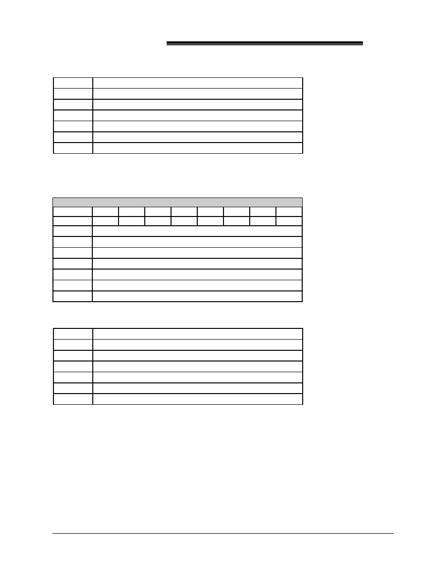
Table 1 summarizes the serial port registers.

2087
ACC Micro
TM
39
Table 1
Serial Port Register Summary
Register
Bit 7
Bit 6
Bit 5
Bit 4
Bit 3
Bit 2
Bit 1
Bit 0
Receiver
Buffer
Register
(read only)
Data
Bit 7 (MSB)
Data
Bit 6
Data
Bit 5
Data
Bit 4
Data
Bit 3
Data
Bit 2
Data
Bit 1
Data
Bit 0 (LSB)
Transmitt-er
Holding
Register
(write onl
only)
Data Bit 7
Data Bit 6
Data Bit 5
Data Bit 4
Data Bit 3
Data Bit 2
Data Bit 1
Data Bit 0
Divisor
Latch (LS)
Bit 7
Bit 6
Bit 5
Bit 4
Bit 3
Bit 2
Bit 1
Bit 0
Divisor
Latch (MS)
Bit 15
Bit 14
Bit 13
Bit 12
Bit 11
Bit 10
Bit 9
Bit 8
Interrupt
Enable
Register
0
0
0
0
Enable
Modem
Status
Interrupt
Enable
Receiver
Line Status
Interrupt
Enable
Transmitt-er
Holding
Register
Interrupt
Enable
Received
Data
Available
Interrupt
Interrupt
Identificatio
n Register
(Read only)
FIFOs
Enabled
FIFOs
Enabled
0
0
0
Interrupt ID
Bit 1
Interrupt ID
Bit 0
"0" IF
Interrupt
Pending
FIFO
Control
Register
(Write only)
RCVR
Trigger
(MSB)
RCSV
Trigger
(LSB)
0
0
0
Reset FIFO
XMIT
Reset FIFO
RCVR
Enable
FIFO
Line Control
Register
Divisor
Latch
Address Bit
Set Break
Stick Parity
Even Parity
Select
Parity
Enable
Number of
Stop Bits
Word
Length
Select Bit 1
Word
Length
Select Bit 0
Modem
Control
Register
0
0
0
Loop
Interrupt
Enable
Not Used
Request to
Send
Data
Terminal
Ready
Line Status
Register
Error in
RCVCR
FIFO
Transmitter
Empty
Transmitter
Holding
Register
Empty
Break
Interrupt
Framing
Error
Parity Error
Overrun
Error
Data Ready
Modem
Status
Register
Data Carrier
Detect
Ring
Indicator
Data Ready
Set
Clear to
Send
Delta
Receive
Line Signal
Detect
Trailing
Edge Ring
Indicator
Delta Data
Set Ready
Delta Clear
to Send
Scratch
Register
Bit 7
Bit 6
Bit 5
Bit 4
Bit 3
Bit 2
Bit 1
Bit 0

2087
ACC Micro
TM
40
Programmable Baud Rate Generator
The serial port interface in the ACC2087 contains a programmable Baud Rate Generator that divides the clock
from DC to 3.1 MHz. Any divisor from 1 to 2
16-1
can be used. The output frequency of the baud rate generator
is 16X the data rate [divisor # = clock + (baud rate x 16)]. The divisor is stored in a 16-bit binary format by two
8-bit divisor latch registers. These divisor latch registers must be loaded during initialization. A 16-bit baud
counter is immediately loaded after either of the divisor latches is loaded to prevent long counts on initial load.
The serial port receiver circuitry in the ACC2087 is programmable for 5, 6, 7 or 8 data bits per character. Word
with less than eight bits are right justified, LSB = Data Bit 0, which is the first data bit received. Unused bits in
a character less than eight bits are output low to the parallel output by the serial port.
Data received at the SIN0(1) (serial input) pin is shifted into the Receiver Shift Register by the clock (16X)
provided at the XIN input. Based on the position of the start bit, this clock is synchronized to the incoming
data.
When a complete character is shifted into the Receiver Shift register, the assembled data bits are loaded in
parallel into the Receiver Buffer Register (RBR). The Data Ready flag in the Line Status register is set.
Transmitter Holding Register (THR) (HEX 3F8 or 2F8, DLAB = 0, W)
Receiver Buffer Register (HEX 3F8 or 2F8, DLAB = 0, R)
The Transmitter Holding Register and Receiver Buffer Register are data registers that hold from five to eight
bits of data. If fewer than eight data bits are transmitted, bit 0 is always the first serial data bit received and
transmitted. Data registers are buffered twice to allow read and write operations to be executed at the same time
the UART is converting parallel to serial and serial to parallel.
The data received is buffered twice to permit continuous data reception without loss of data. As the Receiver
Shift register is shifting a new character into the serial port, the Receiver Buffer register is holding a previously
received character for the CPU. If data in the Receiver Buffer register is not read before complete reception of
the next character, the data in the Receiver register goes low. The overrun condition is flagged by an Overrun
error (Bit 1 of the Line Status register). Table 2 contains Receiver Buffer Register bit definitions.
Table 2 Receiver Buffer Register
Bit
Function
0
Data Bit 0
1
Data Bit 1
2
Data Bit 2
3
Data Bit 3
4
Data Bit 4
5
Data Bit 5
6
Data Bit 6
7
Data Bit 7
The Transmitter Holding Register holds parallel data from the data bus until the Transmitter Shift register is
empty and ready to accept a new character. The receiver word length and transmitter and number of stop bit are
the same. If the character has less than eight bits, unused bits are ignored by the transmitter at the
microprocessor data bus. Table 3 contains the bit definitions of the Transmitter Holding register.
2087
ACC Micro
TM
41
Table 3 Transmitter Holding Register
Bit
Function
0
Data Bit 0 *
1
Data Bit 1
2
Data Bit 2
3
Data Bit 3
4
Data Bit 4
5
Data Bit 5
6
Data Bit 6
7
Data Bit 7
* Bit 0 is the first serial data bit transmitted.
Interrupt Enable Register (IER) (HEX 3F9 or 2F9, DALB = 0, R/W)
The Interrupt Enable Register is a write register that enables the two serial port interrupts independently. The
interrupts activate the interrupt output. All interrupts are disabled by resetting Bits 0-3 of this register.
Interrupts are enabled by setting the appropriate bits of this register high. When interrupts are disabled, the
Interrupt Identification register and the active (high) INTSE0(1) signal is inhibited. All other system functions
operate normally, including the setting of the Line Status register and the Modem Status register. Table 4
contains Interrupt Enable register bit definitions.
Table 4 Interrupt Enable Register
Bit
Function
0
Received Data Available interrupt. = 1 enable; = 0 disable.
1
Transmitter holding register empty interrupt. = 1 enable; = 0 disable.
2
Receiver line status interrupt. = 1 enable; = 0 disable.
3
Modem Status interrupt. = 1 enable; = 0 disable.
4-7
Must be set to logic 0.
Interrupt Identification Register (IIR) (HEX 3FA or 2FA, R)
The Interrupt Identification Register has the interrupt capability to interface to current microprocessors. The
serial port interface prioritizes interrupts into four levels to minimize software overhead during data character
transfer. The four levels of interrupt conditions include
Priority 1
Receiver Line Status
Priority 2
Received Data Ready
Priority 3
Transmitter Holding Register Empty
Priority 4
Modem Status
The Interrupt Identification register stores information that an interrupt is pending and the type of interrupt.
When addressed during chip select time, this register indicates the highest priority interrupt pending. No other
interrupts are acknowledged until the CPU services this interrupt. Table 5 contains Interrupt Identification
register bit definitions. Table 6 contains interrupt identification, set and reset information.

2087
ACC Micro
TM
42
Table 5 Interrupt Identification Register
Bit
Function
0
Indicates a pending interrupt. When this bit is low, an interrupt is pending and the register contents
can be used as a pointer to the appropriate interrupt service routine. When this bit is high, no
interrupt is pending.
1-2
Identifies highest priority pending
3-5
Set to 0. Bit 3 must be set to 0. In FIFO mode, this bit is set along with bit 2 when a time-out
interrupt is pending.
6-7
Enable FIFO. These bits are set when the FIFO Control Register bit 0 is set to one.
Table 6 IIR Interrupt ID, Set and Reset
Interrupt Identification
Interrupt Set and Reset Functions
Bit
3
Bit2
Bit1
Priorit
y
Bit 0
Level
Interrupt
Flag
Interrupt
Source
Interrupt
Reset Control
0
x
x
1
None
None
0
1
1
0
1
Receiver line status
OE, PE, FE, or BI
LSR Read
0
1
0
0
2
Received data
available
Received data available RBR Read or
the FIFO
drops below
the trigger
level
1
1
1
0
2
Character Time-out
Atleast one character is
in the FIFO and no
characters have been
read from or input to
the FIFO during the
last 4 character times
RBR Read
0
0
1
0
3
THRE
THRE
IIR Read if
THRE is the
interrupt
source or
THR write
0
0
0
0
4
Modem status
CTS0#(1), DSR0#(1).
RI0#(1), RLSD0#(1).
MSR Read
x = not defined

2087
ACC Micro
TM
43
FIFO Control Register (HEX 3FA or 2FA, W)
Bit
Function
0
Enable FIFO. When set to 1, bit 1, 2 is enabled. Resetting this bit will cleared all bytes in both
FIFOs.
1
Reset FIFO Receiver. When set to 1, it clears all bytes in the receiver FIFO. Its logic counter will
be reset to 0.
2
Reset FIFO Transmitter. When set to 1, it clears all bytes in the Transmitter FIFO. Its logic counter
will be reset to 0.
3
Set to 0.
4-5
Set to 0
6
Trigger Receiver (LSB). This bit is used to set the trigger level for the receiver FIFO.
7
Trigger Receiver (MSB). This bit is used to set the trigger level for the receiver FIFO.
7 6 RCV FIFO Trigger Level (Bytes)
0 0 1
0 1 4
1 0 8
1 1 14
Address, Read, and Write inputs are used with the Divisor Latch Access bit (DLAB) in the Line Control register
bit 7 [LCR(7)] to select the register to be read or written. Refer to Table 7 for register select states.
Table 7
Serial Port Internal Register Selection
DLAB
A2
A1
A0
Register
0
0
0
0
Receiver buffer register (read only)
0
0
0
0
Transmitter holding register (write only)
0
0
0
1
Interrupt enable register
x
0
1
0
Interrupt identification register (read only)
x
0
1
1
Line control register
x
1
0
0
Modem control register
x
1
0
1
Line status register
x
1
1
0
Modem status register
x
1
1
1
Scratch register
1
0
0
0
Divisor latch (LSB)
1
0
0
1
Divisor latch (MSB)
x = Don't care
Note that the serial port is accessed only when internal chip select signal CSSE0#(1) is low.
Line Control Register (LCR) (HEX 3FB or 2FB, R/W)
The Line Control Register controls the format of a data character. The contents of the LCR can be read
precluding the need to store line characteristics in system memory. Table 8 contains the contents of the Line
Control register.

2087
ACC Micro
TM
44
Table 8
Line Control Register
Bit
Function
Logic 1
Logic 0
0
Word length select Bit 0
1
Word length select Bit 1
2
Stop bit select
1.5 or 2 stop bits
1 stop bit
3
Parity enable
Enabled
Disabled
4
Even parity select
Even parity
Odd parity
5
Stick parity
Enabled
Disabled
6
Set break
Enabled
Disabled
7
Divisor latch access bit
Bit 0-1 The number of bits in each serial character is programmed according to the following states.
LCR(1)
LCR(0)
Word length
0
0
5 bits
0
1
6 bits
1
0
7 bits
1
1
8 bits
Bit 2
Specifies the number of stop bits in each character transmitted. If Bit 2 = 0, one stop bit is generated
or checked in the transmitted data. If Bit 2 = 1 when a 5-bit word is selected, 1.5 stop bits are
generated. If Bit 2 = 1 when a 6-, 7- or 8-bit word is selected, two stop bits are generated. The
receiver checks the first stop bit only regardless of the number of stop bits selected.
Bit 3
When high, generates and checks a parity bit between the last data word bit and stop bit of the serial
data.
Bit 4
When parity is enabled (Bit 3 = 1), and Bit 4 = 0, odd parity is selected. When parity is enabled and
Bit 4 = 1, even parity is selected.
Bit 5
When parity is enabled and Bit 5 = 1, a parity bit is transmitted and received in the opposite state
from the state indicated by Bit 4. Parity can therefore be forced to a known state and the receiver
can check the parity bit in a known state.
Bit 6
When set to 1, serial output is forced to the spacing (logic 0) state. The break is disabled when this bit
is set to 0. Bit 6 acts only on serial output and has no effect on the transmitting logic. Bit 6 enables
the CPU to alert a terminal in a computer system. If the following sequence is used, no erroneous or
extraneous characters are transmitted because of the break.
1.
Load an all zeros, pad character, in response to Line Status register Bit 5.
2.
Set break in response to the next Line Status register Bit 5.
3.
Wait for the transmitter to become idle (Line Status register Bit 6), and clear break
when normal transmission must be restored.
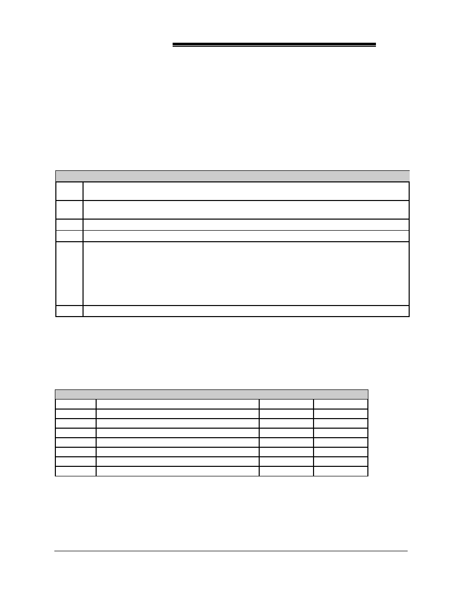
2087
ACC Micro
TM
45
Bit 7
Must be set high to access the Divisor latches DLL and DLM of the Baud rate generator during a
read or write operation. This bit must be input low to access the Receiver buffer, the Transmitter
holding, or the Interrupt enable registers.
Modem Control Register (MCR) (HEX 3FC or 2FC, R/W)
The Modem Control Register controls the interface with the modem or data set. This register can be read or
written. Table 9 contains Modem Control register bit definitions.
Table 9
Modem Control Register
Bit
Function
0
Data terminal ready (DTR). When set to 1, the Data terminal ready [DTR0#(1)] output is forced to a
logic 0. When this bit is reset to a logic 0, DTR0#(1) output is forced to a logic 1.
1
Request to send (RTS). When set to 1, the Request to send [RTS0#(1)] output is forced to a logic 0.
When this bit is reset to a logic 0, RTS0#(1) output is forced to a logic 1.
2
Not used.
3
Interrupt enable. When set high, Serial port interrupt (SIRQ3, SIRQ4) output is enabled.
4
Loopback..This bit provides a local loopback feature to perform diagnostic testing of the channel.
When set high, SOUT0(1) is set to the marking state (logic 1), and the receiver data input Serial
Input [SIN0(1)] is disconnected. The output of the Transmitter Shift register is looped back into the
Receiver Shift register input. The four modem control inputs are disconnected. Modem control
outputs are connected to the four modem control inputs internally. Modem control output pins are
forced to the high (inactive state). In the diagnostic mode, data transmitted is received immediately
so the processor can verify the transmit and receive data paths of the selected serial port.
5-7
0
Line Status Register (LSR) (HEX 3FD or 2FD, W/R)
The Line Status Register is usually the first register read by the CPU to determine the cause of an interrupt or to
poll the status of the serial port interface. Refer to Table 10 for bit definitions.
Table 10
Line Status Register
Bit
Function
Logic 1
Logic 0
0
Data ready (DR)
Ready
Not ready
1
Overrun error (OE)
Error
No error
2
Parity error (PE)
Error
No error
3
Framing error (FE)
Error
No error
4
Break interrupt (BI)
Break
No break
5
Transmitter holding register empty (THRE)
Empty
Not empty
6
Transmitter empty (TEMT)
Empty
Not empty
7
Not used

2087
ACC Micro
TM
46
Bits 1-4 are the error conditions that produce a Receiver Line Status interrupt (priority 1 interrupt in the
Interrupt Identification register). This interrupt is enabled by setting the Interrupt Enable register Bit 2
to 1. Bits 1-4 are cleared when the Line Status register is read.
Bits 1-3 are three error flags that provide the status of an error condition detected in the receiver circuitry:
Overrun error, Framing error, and Parity error. Error flags are set high by an error condition when stop
bits are received.
Bit 0
This bit is set high when an incoming character is received and transferred into the Receiver Buffer
register or the FIFO. It will reset to low after reading all of the data in the RBR or the FIFO.
Bit 1
Overrun error means that the Receiver Buffer register was not read by the CPU before the next
character was transferred into the Receiver Buffer register, overwriting the previous character. This bit
is reset when the CPU reads the contents of the Line Status register.
Bit 2
A parity error means that the last character received had a parity error based on the programmed and
calculated parity of the received character (Line Control register Bit 4).
Bit 3
A framing error means that the last character received had incorrect (low) stop bits (caused when
the required stop bit is absent or by a stop bit too short to be detected). This bit is high when the stop
bit following the last data bit or parity bit is detected as a zero bit (spacing level). This bit is reset low
when the CPU reads the contents of the Line Status register.
Bit 4
This bit indicates that the last character received was a break character. A break character is defined as
an invalid but complete data character, including parity and stop bits. This bit is set high when the
received data input is held in the spacing (logic 0) state for a longer time than a full word transmission
time (start bit + data bits + parity + stop bits). Bit 4 is reset when the CPU reads the contents of the
Line Status register.
Bit 5
This bit indicates that the Transmitter Holding register is empty and can receive another character. If
the interrupt is enabled (Interrupt Enable register Bit 1), this bit when active causes an interrupt. The
interrupt is cleared when the Interrupt Identification register is read. Bit 5 is set high when a character
is transferred from the Transmitter Holding register into the Transmitter Shift register. This bit is reset
low when the CPU loads the Transmitter Holding register. Bit 5 is NOT reset when the CPU reads the
Line Status register.
Bit 6
This bit is set high when the Transmitter Holding register and the Transmitter Shift register are both
empty. When a character is loaded into the Transmitter Holding register, this bit is set low and remains
low until the character is transferred out of SOUT0(1) (Serial output pin). Bit 6 is NOT reset when the
CPU reads the Line Status register.
Bit 7
This bit is always zero.

2087
ACC Micro
TM
47
Modem Status Register (MSR) (HEX 3FE or 2FE, R/W)
The Modem Status Register provides the CPU with the status of the modem input lines from the modem or
peripheral devices. The CPU can read the serial port modem signal inputs by accessing the data bus interface of
the ACC2087. Four bits in this register indicate if the modem inputs have changed since the last read of the
Modem status register. These bits are set high when a control input from the modem changes state. When the
CPU reads the Modem Status register, these bits are reset low.
The CTS0#(1), DSR0#(1), RI0#(1) and RLSD0#(1) signals are the modem input lines for the channel. Bits 4
through 7 are status indications of these lines. If the modem status interrupt in the Interrupt Enable register Bit
3 is enabled, a change of state in a modem input signals is reflected by the modem status bits in the IIR register
and an interrupt is generated. The Modem Status register is a priority 4 interrupt. Refer to Table 11 for bit
definitions. Note that the state of the status bit is an inverted version of the actual input pin.
Table 11
Modem Status Register
Bit
Function
0
Delta clear to send. Indicates that CTS0#(1) input to the serial port interface has changed state since
the last time it was read by the CPU.
1
Delta data set ready. Indicates that DSR0#(1) input to the serial port interface has changed state
since the last time it was read by the CPU.
2
Trailing edge of ring indicator. Indicates that RI0#(1) input to the serial port interface has changed
state since the last time it was read by the CPU. Low to high transitions on Bit 6 do not activate this
bit.
3
Delta data carrier detect. Indicates that RLSD0#(1) input to the serial port interface has changed
state since the last time it was read by the CPU.
4
Clear to send. This bit is the complement of CTS0#(1) input from the modem. This input tells the
serial port that the modem is ready to receive data from the transmitter output of the serial port. If
the serial port interface is in loop mode (Modem Control register Bit 4 = 1), this bit is equivalent to
Modem Control register Bit 1 (request to send).
5
Data set ready. This bit is the complement of the DSR0#(1) input from the modem to the serial port.
This input tells the CPU that the modem is ready to provide received data to the serial port receiver
circuitry. If the channel is in loop mode (Modem Control register Bit 4 = 1), this bit is equivalent to
Modem Control register Bit 0 (data terminal ready).
6
Ring indicator. This bit is the complement of the RI0#(1) pin. If the channel is in loop mode
(Modem Control
register Bit 4 = 1), this bit is not connected in the Modem Control register.
7
Data carrier detect. This bit is the complement of receiver line detect signal input and is equivalent
to Modem control register Bit 3.
Modem status inputs reflect the modem input lines with any change of status. Reading the Modem Status
register clears the delta modem status indications but does not affect the status bits. The status bits reflect the
state of the input pins regardless of mask control signals. If bits 0-3 are true, and a state change occurs during a
read operation, the state change is not reflected in the Modem Status register. If bits 0-3 are false, the state
change is indicated after the read.
Setting status bits is inhibited for the Line Status register and Modem Status register during status read
operations. If a status condition is generated during a CPU read, the status bit is not set until the trailing edge
of the read.
If a status bit is set during a read operation, and the same status condition occurs, that status bit is cleared at the
trailing edge of the read instead of being set again.

2087
ACC Micro
TM
48
Scratch Register (SR) (HEX 3FF or 2FF, R/W)
The Scratch Register is an 8-bit Read/Write register. This register does not affect either channel in the serial
port. It is used by programmers to hold data temporarily. Table 12 contains bit definitions.
Table 12
Scratch Register
Bit
Function
0
Data Bit 0
1
Data Bit 1
2
Data Bit 2
3
Data Bit 3
4
Data Bit 4
5
Data Bit 5
6
Data Bit 6
7
Data Bit 7
Transmitting
The serial port interface transmitting function includes the Transmitter Holding register, Transmitter Shift
register, and the associated control logic. Bits 5 and 6 in the Line Status Register indicate the status of the
Transmitter Holding register and the Transmitter Shift register. To transmit a 5- to 8-bit word, the word is
written to the Transmitter Holding register through SD0-SD7. The microprocessor performs a write operation
only if it is transmitted.
Bit 5 of the Line Status register is high when the word is automatically transferred from the Transmitter
Holding register to the Transmitter Shift register when the start bit is transmitted.
When the transmitter is idle, Bits 5 and 6 of the Line Status register are high. The first word written causes Bit
5 to be reset to zero. After the transfer, Bit 5 return high. Bit 6 remains low while the data word is transmitted.
If a second character is transmitted to the Transmitter Holding register, Bit 5 of the Line Status register is reset
low. Because the data word cannot be transferred from the Transmitter Holding register to the Transmitter Shift
register until its empty, Bit 5 of the Line Status register remains low until the word is completely transmitted.
When the last word is transmitted out of the Transmitter Shift register, Bit 6 of the Line Status register is set
high. Bit 5 of the Line Status register is set high one transfer time later.
Receiving
Serial asynchronous data is input into SIN0(1) (Serial Input pin). The idle state of the line providing the input
into the SIN pin is high. Start bit detection circuitry continually searches for a high to low transition. When a
transition is detected, a counter is reset. Count is the 16X clock to 7 1/2, which is the center of the start bit. If
the SIN signal is still low at the mid-bit sample of the start bit, the start bit is considered valid. By verifying the
start bit, the receiver is prevented from assembling a false data character caused by a low going noise spike on
the Serial Input pin.
The Line Control register determines the number of data bits in a character, the number of stop bits, if parity is
used, and the polarity of parity. The Line Status register provides status for the receiver to the Receiver Buffer
register. The data received (indicated by Bit 0 of the Line Status register) is set high. The CPU reads the
Receiver Buffer register through SD0-SD7. This read resets Bit 0 of the Line Status register. If a character is
not read before a new character transfer from the Receiver Status register to the Receiver Buffer register, the
overrun error status bit is set (Line Status register Bit 1). The parity check looks for even or odd parity on the

2087
ACC Micro
TM
49
parity bit which precedes the first stop bit. The parity error is set in Line Status register Bit 2 if an error is
detected. If the stop bit is not high, a framing error is indicated by Line Status register Bit 3.
The center of the start bit is defined as clock count 7 1/2. If the data received by the Serial Input pin is a
symmetrical square wave, the center of the data cells occurs within +/- 3.125% of the mid-point. This is a
46.875% error margin. The start bit can begin as much as one 16X clock cycle before it is detected.
Baud Rate Generator
The Baud Rate generator generates clocking for the UART function and provides standard ANSI/CCITT bit
rates.
An external clock into CLK provides the oscillator driving the Baud Rate generator.
The Divisor Latch registers DLL and DLM, and external frequency determine the data rate. The bit rate is
selected by programming the two divisor latches. When DLL is set to 1, and DLM is set to 0, the divisor
divides by 1 (provides maximum baud rate for a given input frequency at the CLK input). Table 13 shows the
baud rate for 1.8432 Clock.
Table 13
Baud Rates for 1.8432 MHz Clock
Baud Rate
Divisor
50
2304
75
1536
110
1047
134.5
857
150
768
300
384
600
192
1200
96
1800
64
2000
58
2400
48
3600
32
4800
24
7200
16
9600
12
19200
6
38400
3
56000
2

2087
ACC Micro
TM
50
Resetting
The RESET# input must be held low for 500 ns to reset the serial port circuits to an idle mode until
initialization. A low state on the RESET# signal causes the following events.
1.
Initializes the transmitter and receiver internal clock counters.
2.
Clears the Line Status register except Bits 5 and 6 which are set. Also clears the Modem Control
register. All discrete lines, memory elements and logic associated with these registers are also cleared
or turned off. The Line Control register, Divisor latches, Receiver Buffer register and Transmitter
Buffer register are not affected.
After the rest condition is removed, the serial port remains idle until programmed. A hardware reset sets Bits 5
and 6 of the Line Status register. When interrupts are enabled, Bit 5 activates the interrupt. Refer to Table 14
for summary of reset effects.
Table 14
Reset Summary
Register/Signal
Reset Control
Reset
Interrupt Enable Register
Reset
All bits low (0-3 forced and 4-7
permanent)
Interrupt Identification Register
Reset
Bit 0 is high, Bits 1-2 low
Bits 3-7 are permanently low
Line Control Register
Reset
All bits low
Modem Control Register
Reset
All bits low
Line Status Register
Reset
Bits 0-4 and 7 are low, Bits 5-6
high
Modem Status Register
Reset
Bits 0-3 low, Bits 4-7 input
signal
Serial Output (SOUT)
Reset
High
Interrupt (Receiver line status)
Read LSR/Reset
Low
Interrupt (Receiver data available)
Read RBR/Reset
Low
Interrupt (THRE)
Read IIR/Write THR/Reset
Low
Interrupt (Modem Status)
Read MSR/Reset
Low
RTS#
Reset
High
DTR#
Reset
High
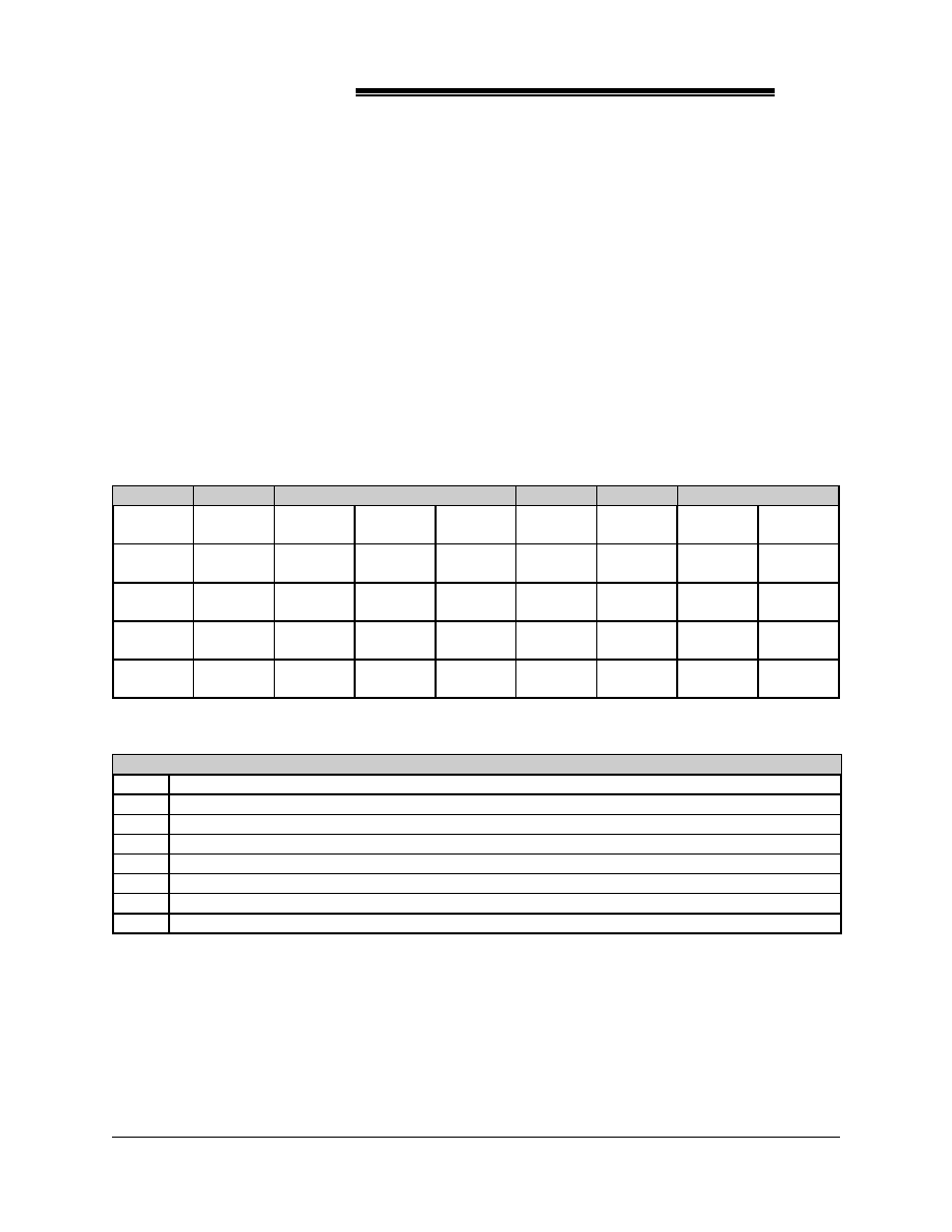
2087
ACC Micro
TM
51
2.33 Parallel Port Interface
The parallel port interface in the ACC2087 provides compatibility for a Centronics type printer. Its
configuration register allows the parallel port to be configured in PS/2 type bi-directional parallel port and
Extended Capabilities Port (ECP) modes. Table 15 lists the registers associated with the parallel port interface.
The address map of the parallel port is shown below:
Data Port
=
Base Address + 00H
Status Port
=
Base Address + 01H
Control Port
=
Base Address + 02H
The microprocessor reads information on the parallel bus through Read Data register. The read and write
functions of a register are controlled by the state of the read pin (IOR#) and write pin (IOW#).
The microprocessor reads the status of the printer in the five most significant bits of the Read Status register.
Table 16 contains the bit definitions for this register.
Table 15
Parallel Port Interface Register Summary
Register
Bit 7
Bit 6
Bit 5
Bit 4
Bit 3
Bit 2
Bit 1
Bit 0
Read
Data
PD7
PD6
PD5
PD4
PD3
PD2
PD1
PD0
Read
Status
BUSY#
ACK#
PE
SLCT
ERROR#
1
1
1
Read
Control
1
1
1
IRQENB
SLIN
INIT#
AUTOF
D
STROBE
Write
Data
PD7
PD6
PD5
PD4
PD3
PD2
PD1
PD0
Write
Control
1
1
0
IRQENB
SLIN
INIT#
AUTOF
D
STROBE
Table 16
Read Status Register
Bit
Function
0
1
1
1
2
1
3
Error
4
Printer select
5
Paper Empty
6
Acknowledge
7
Printer busy
The Read Control Register is for reading the state of the control lines. The Write Control Register sets the state
of the control lines. Table 17 contains the bit definitions for the Write Control Register.
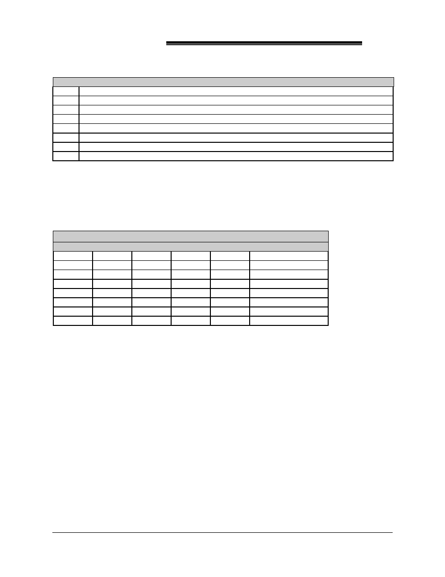
2087
ACC Micro
TM
52
Table 17
Write Control Register
Bit
Function
0
Strobe to inform the printer of the presence of a valid byte on the parallel port
1
Autofeed the paper
2
Initialize the printer
3
Select IN
4
Interrupt enable
5
Direction
6
Must be set to 1
7
Must be set to 1
Decoder
The parallel port address decoder selects registers according to the states of the signals listed in Table 18.
Table 18
Address Decoder Register Selection
Control Signals
IOR#
IOW#
CSPA#
*A1
A0
Register Selected
0
1
0
0
0
Read Data register
0
1
0
0
1
Read Status register
0
1
0
1
0
Read Control register
0
1
0
1
1
Invalid
1
0
0
0
0
Write Data register
1
0
0
0
1
Invalid
1
0
0
1
0
Write Control register
1
0
0
1
1
Invalid
* CSPA# is an internal signal to parallel port logic.

2087
ACC Micro
TM
53
Extended Capability Port (ECP)
The ECP mode is also supported by the ACC ACC2087 with a 16bytes FIFO. The address map and ECP
register configuration of the ECP are shown below:
Address Map: (Base Address = 278h or 378h)
Data Port
:
Base Address + 000h
ECPAFIFO
:
Base Address + 000h
DSR
:
Base Address + 001h
DCR
:
Base Address + 002h
ECPCFIFO
:
Base Address + 400h
ECPDFIFO
:
Base Address + 400h
TFIFO
:
Base Address + 400h
CNFGA
:
Base Address + 400h
CNFGB
:
Base Address + 401h
ECR
:
Base Address + 402h
ECP Register Configuration:
ECPAFIFO - ECP FIFO Address / RLE (Mode 011)
Bit
Description
7
Write only. This bit is used to indicate data type.
When set to 1, bits [6:0] are a ECP address.
When set to 0, bit field [6:0] is a run length. It is used to indicate how many times the next data will
be appeared. ( for example: [6:0] = 0 is 1 time, [6:0] = 1 is 2 times, [6:0] = 2 is 3 times, etc.
6-0
Write only. This is a ECP address or run length encode (RLE) as described above.

2087
ACC Micro
TM
54
DSR - Device Status Register (Mode All)
Bit
Description
7
Read only. nBUSY. This indicates a inverted version of parallel port BUSY signal.
6
Read only. nACK. This indicates a version of parallel port nACK signal.
5
Read only. PERROR. This indicates a version of parallel port PERROR signal.
4
Read only. SELECT. This indicates a version of parallel port SELECT signal.
3
Read only. nFAULT. This indicates a version of parallel port nFAULT signal.
2-0
Reserved.
DCR - Device Control Register (Mode All)
Bit
Description
7-6
Reserved.
5
Read/Write. Direction.
When set to 0, DMA and data are written to the peripheral. The drivers are enabled.
When set to 1, if it is in standard parallel port mode (mode 000 or 010), this bit has no effect. If it is
in ECP mode, the drivers is tri-stated and it sets the direction so that data will be read from the
peripheral.
4
Read/Write. When set to 0, it disables the nACK interrupt. When set to 1, it enables an interrupt on
the rising edge of nACK.
3
Read/Write. When set to 0, this bit has no effect. When set to 1, it forces the SELECTIN signal low
regardless of the hardware state machine even in ECP mode. Software should make sure that bit 3 is
set to 0 prior to entering ECP mode.
2
Read/Write. When set to 0, this bit has no effect. When set to 1, it forces the nINIT signal active
regardless of the hardware state machine.
1
Read/Write. When set to 0, this bit has no effect. When set to 1, it forces the AUTOFD signal low
regardless of the hardware state machine even in ECP mode. Software should make sure that bit 1 is
set to 0 prior to entering ECP mode.
0
Read/Write. When set to 0, this bit has no effect. When set to 1, it forces the STROBE signal low
regardless of the hardware state machine even in ECP mode. Software should make sure that bit 0 is
set to 0 prior to entering ECP mode.
CFIFO - Parallel Port Data FIFO (Mode 011)
This mode is only defined for forward direction. The hardware standard parallel port protocol is used to
transmit the bytes written or DMAed, from the system to this FIFO, to the peripheral. Transfers to the FIFO are
bytes aligned.
ECPDFIFO - ECP Data FIFO (Mode 011)
When DCR (Device Control Register) bit 5 is set to 0, the hardware ECP parallel port protocol is used to
transmit the bytes written or DMAed , from the system to this FIFO, to the peripheral. Transfer to the FIFO are
bytes aligned. When DCR bit 5 is set to 1, data from the peripheral are read under automatic hardware
handshake from ECP into the FIFO.

2087
ACC Micro
TM
55
TFIFO - Test Mode (Mode 110)
Data may be read, written or DMAed to or from the system to this FIFO in any direction.
Data in the TFIFO will not be transmitted to the parallel port lines using a hardware protocol handshake,
However, data in the TFIFO may be displayed on the parallel port data lines.
The TFIFO will not stall when overwritten or underrun. Data will simply be re-written or over-run. The full
and empty bits must always keep track of the correct FIFO state. The TFIFO will transfer data at the maximum
ISA rate so that software may generated performance metrics.
Data PWords are always read from the head of TFIFO regardless of the value of the direction bit. The FIFO
size and interrupt threshold can be determined by writing PWords and checking the full and service interrupt
bits.
CNFGA - Configuration Resister A (Mode 111)
This is a read only register.
CNFGB - Configuration Register B (Mode 111)
Bit
Description
7
Reserved. Always 0.
6
Read only. Its value on the ISA interrupt line determines the possible conflicts. Default 1.
5-0
Reserved. Always 0.
ECR - Extended Control Register
Bit
Description
7-5
Read/Write.
When set to 000, the standard parallel port mode is selected. In this mode the FIFO is reset and
common collector drivers are used on the control lines. Setting the direction bit will not tri-state the
output drivers in this mode.
When set to 001, the PS/2 parallel port mode is selected. This is the same as the standard parallel
mode except that direction may be used to tri-state the data lines and reading the data register returns
the value on the data lines and not the value in the data register.
When set to 010, the parallel port FIFO mode is selected. This is the same as the standard parallel
port mode except that PWords are written or DMAed to the FIFO. FIFO data is automatically
transmitted using the standard parallel port protocol. Note that this mode is only useful when
direction is 0. All drivers have active pull-ups.
When set to 011, the ECP parallel port mode is selected. In the forward direction PWords placed
into the ECPDFIFO and bytes written to the ECPAFIFO are placed in a single FIFO and transmitted
automatically to the peripheral using ECP protocol. In the reverse direction bytes are moved from
the ECP parallel port and packed into PWords in the ECPDFIFO.
When set to 110, the test mode is selected.
When set to 111, configuration register A,B are accessible at 0x400 and 0x401.
When set to 100, it is reserved.

2087
ACC Micro
TM
56
Section 3
3.1 2087 Pin Description
Table 3-1 Clock Interface
Pin Name
Pin #
Type
Description
CLKSRC
70
I
System clock source. It is an input clock from the CMOS
oscillator or clock chip.
SYSCLK
34
O
Peripheral or AT bus clock. This clock can be derived from
either X14M or CLKSRC to provide a system clock source
for the AT Bus.
CLKI
48
I
System input clock. It in an input clock buffer from either
CLKX1 or
CLKX2 feedback to CLKI.
X14M
141
I
14.318 MHz crystal input.
CLKX1
51
O
CLKX1 = CLKSRC divided by 2.
CLKX2
49
O
CLKX2 = CLKSRC divided by 1.
Table 3-2 Reset Interface
Pin Name
Pin #
Type
Description
PWRGD
77
I
"Power Good" signal from the power supply. It must be
stabled for at least 1ms.
CPURST
30
O
CPU reset output.
RESETDRV
213
O
System reset. Active high. This reset signal is for the bus
devices to reset or initialize system logic upon power-up or
during a low line voltage. This signal is deasserted at phase 2.

2087
ACC Micro
TM
57
Table 3-3 CPU Interface
Pin Name
Pin #
Type
Description
ADS#
74
I/O
ADS# is driven directly by the CPU ADS# pin. It is asserted
in T1 of the CPU bus cycle.
M/-IO
41
I/O
When high, it is indicates current bus cycle is a memory
access cycle. It is an I/O cycle when it is low.
D/-C
42
I/O
It indicates whether the current bus cycle is a data or control
cycle.
W/-R
43
I/O
It indicates whether the current bus cycle is a read or write
cycle.
RDY#
37
I/O
This is a ready signal to CPU. It becomes an input in local
bus cycle.
BRDY#
44
O
It indicates to the CPU the data for (read/write) cycle is ready.
HITM#
FLUSH#
93
I
Asserted by the CPU to indicate a snoop cycle hit a modified
line and needs to be written back.
EADS#
LA20
98
O
I
When this pin is pulled low during power on, it indicates a
valid external address has been driven onto the processor
address pins to be used for an inquire cycle.
If this pin is pulled high during power on, it becomes the AT
slot A20 signal through a 245 transceiver.
GA20
92
O
It is used to force the CPU to mask off A20 in real mode
applications.
PHOLD
35
O
CPU hold request.
/KTGOE
58
O
This pin is the cache tag output enable signal /KTOEN.

2087
ACC Micro
TM
58
Table 3-3 CPU Interface contd..
Pin Name
Pin #
Type
Description
HLDA
128
I
It indicates that the CPU has granted the control of the bus in
response to PHOLD.
KEN#
36
O
It indicates that the current cycle is cacheable.
SMIACT#
SMIADS#
134
I
It indicates by the CPU that it is in system management mode
after SMI# being served by the CPU.
SMI#
126
O
It is used to invoke the system management mode (SMM).
STPCLK#
125
O
It indicates a request to stop the CPU clock for power
management control.
SUSPACK#
228
I
This suspend acknowledge signal is used to support Cyrix
CPU.
A2-A25, A31
59-68
72,73
78-90
I/O
These are input during CPU cycles. These become output
during cache cycle.
D0-15
153-162
164-169
I/O
CPU data bus.
BE#[3:0]
94-97
I/O
These are used to indicate which byte lanes the CPU cycle is
accessing
NMI
32
O
Non-Maskable Interrupt. It connects to the NMI of the CPU.
INTR
40
O
Interrupt indicates a valid interrupt request is asserted.
NPERR
75
I/O
Numeric Coprocessor Error. It indicates a coprocessor error.
IGNNE#
CPUBZY#
39
O
Ignore Error.
BLAST#
NPEREQ
76
I
It indicates the last transfer of a multiple transfer cycle.
BS16#
O
It indicates to the CPU that it requests a 16-bit data bus
transfer (not a 32-bit transfer).
/READYO
/LBA
127
I
This is a multifunction pin, when Register 1B, bit 4 is set to
one, this pin becomes the /LBA pin to sense the existence of
local bus peripherals . When set to zero, this pin is the
Coprocessor Ready input to 2087.

2087
ACC Micro
TM
59
Table 3-4 Power Management / Cache / DRAM / AT Multiplex Interface
Pin Name
Pin #
Type
Description
PWRCNTL0
KWEB
57
O
I/O
In notebook mode, this is a power control pin.
In desktop mode, this pin becomes cache write enable for
bank B.
PWRCNTL1
KOEB
56
O
O
In notebook mode, this is a power control pin.
In desktop mode, this pin becomes cache output enable for
bank B.
PWRCNTL2
MDLATCH
52
O
O
In notebook mode, this is a power control pin.
In desktop mode, this pin becomes MD latch to support
posted write function.
PWRCNTL3
DAC2
150
O
O
In notebook mode, this is a power control pin.
In desktop mode, this pin becomes DAC2.
PWRCNTL4
DRQ1
203
O
I
In notebook mode, this is a power control pin.
In desktop mode, this pin becomes DMA request 1.
PWRCNTL5
DRQ3
204
O
I
In notebook mode, this is a power control pin.
In desktop mode, this pin becomes DMA request 3.
PWRCNTL6
DRQ6
206
O
I
In notebook mode, this is a power control pin.
In desktop mode, this pin becomes DMA request 6.
PWRCNTL7
DRQ7
207
O
I
In notebook mode, this is a power control pin.
In desktop mode, this pin becomes DMA request 7.
ACPWR
PAR0
151
I
I/O
In notebook mode, this is an AC power input. ACPWR is a
active high pin.
In desktop mode, this pin becomes parity check 0.
ALARM
PAR1
152
I
I/O
In notebook mode, this is an alarm input. ALARM is a active
high pin.
In desktop mode, this pin becomes parity check 1.
LBAT1#
PAR2
173
I
I/O
In notebook mode, this is a low battery input. LBAT# is a
active low pin.
In desktop mode, this pin becomes parity check 2.
2087
ACC Micro
TM
60
Table 3-4 Power Management / Cache / DRAM / AT Multiplex Interface contd..
EXTSYS#
PAR3
174
I
I/O
In notebook mode, this is an external system event.
EXTSYS# is a active low pin.
In desktop mode, this pin becomes parity check 3.
EXTSMI1
IOCHK
130
I
I
In notebook mode, this is a external SMI signal. EXTSMI1
is a low to high edge triggered.
In desktop mode, this pin becomes AT bus IO check signal.
STPGNT#
IRQ13
225
O
I
In notebook mode, this pin output a zero in grant bus cycle.
In desktop mode, this pin becomes interrupt 13.
SUSPMOD#
IRQ15
227
O
I
In notebook mode, this pin indicates that the system enters
suspend mode.
In desktop mode, this pin becomes interrupt 15.
DACK0
DAC0
148
I/O
O
In notebook mode, this is DMA acknowledge 0.
In desktop mode, this pin becomes DAC0.
DACK5
DAC1
149
I/O
O
In notebook mode, this is DMA acknowledge 5.
In desktop mode, this pin becomes DAC1.
Note: The DAC1-DAC2 's strapping condition during power-on will set the ACC2087 to either desktop or
notebook mode.
PIN#
DESKTOP MODE
DAC2 = 0, DAC1 = 0
NOTEBOOK MODE1
DAC2 = 0, DAC1 = 1
NOTEBOOK MODE2
DAC2 = 1, DAC1 = 0
151
PAR0
ACPWR
ACPWR
152
PAR1
ALARM
ALARM
173
PAR2
BATLOW
BATLOW
174
PAR3
EXTSYS
EXTSYS
55
KWEA
KWE
KWE
54
KOEA
KOE
KOE
57
KWEB
PWRCNTL0
PWRCNTL0
56
KOEB
PWRCNTL1
PWRCNTL1
52
MDLATCH
PWRCNTL2
PWRCNTL2
225
IRQ13
STPGNT
STPGNT
227
IRQ15
SUSPEND
SUSPEND
148
DAC0
DACK0
DAC0
149
DAC1
DACK5
DAC1
150
DAC2
PWRCNTL3
DAC2
203
DRQ1
PWRCNTL4
DRQ1
204
DRQ3
PWRCNTL5
DRQ3
206
DRQ6
PWRCNTL6
DRQ6
207
DRQ7
PWRCNTL7
DRQ7
130
IOCHK
EXTSMI1
IOCHK
Table 3-5 Dedicated Power Management Interface
Pin Name
Pin #
Type
Description
EXTSMI0
137
I
This pin indicates a external SMI input. EXTSMI0 is a low
to high edge triggered.
SRBTN#
138
I
This pin is the suspend/resume input button. It is a low to
high edge triggered.

2087
ACC Micro
TM
61
Table 3-6 Dedicated Cache Interface
Pin Name
Pin #
Type
Description
DTYWE#
KTGWE#
38
O
This pin is used as a dirty bit write back enable or tag ram
write enable for level 2 write back cache implementation.
KRMOE#
54
I/O
This pin indicates cache output enable for SRAM. Active
low.
KRMWE#
55
I/O
This pin indicates cache write enable. Active low.
TGLA2
45
O
This pin is toggles Address bit 2.
TGLA3
46
O
This pin is toggle Address bit 3.
TAG0
MA0
ROMCS#
101
I/O
This pin is a multiplexed pin. In cache cycle this is TAG IO.
When in memory cycle, this pin is DRAM Address bit 0.
When in AT bus cycle, this pin is ROM output enable.
TAG1
MA1
CS8042#
102
I/O
This pin is a multiplexed pin. In cache cycle this is TAG IO.
When in memory cycle, this pin is DRAM Address bit 1.
When in AT cycle, this pin is keyboard chip select.
TAG2
MA2
RTCDS#
103
I/O
This pin is a multiplexed pin. In cache cycle this is TAG IO.
When in memory cycle, this pin is DRAM Address bit 2.
When in AT cycle, this pin is Real Time Clock DS
TAG3
MA3
RTCWR#
105
I/O
This pin is a multiplexed pin. In cache cycle this is TAG IO.
When in memory cycle, this pin is DRAM Address bit 3.
When in AT cycle, this pin is Real Time Clock WR.
TAG4
MA4
HCS0#
106
I/O
This pin is a multiplexed pin. In cache cycle this is TAG IO.
This pin is DRAM Address bit 4. In AT cycles, HCS0# is
active for addresses 1F0h-1F7h or 170h-177h.
TAG5
MA5
HCS1#
107
I/O
This pin is a multiplexed pin. In cache cycle this is TAG IO.
This pin is DRAM Address bit 5. In AT cycles, HCS1# is
active for addresses 3F6h-3F7h or 376h-377h.
TAG6
MA6
IENH#
108
I/O
This pin is a multiplexed pin. In cache cycle this is TAG IO.
In DRAM cycles, this pin is DRAM Address bit 6. In AT
cycles, this pin is IDE Bus Transceiver High Byte Enable.
TAG7
MA7
IENL#
109
I/O
This pin is a multiplexed pin. In cache cycle this is TAG IO.
In DRAM cycles, this pin is DRAM Address bit . In AT
cycles, this pin is IDE Bus Transceiver Low Byte Enable.
TAG8
MA8
WRPWRCLT1#
110
I/O
This pin is a multiplexed pin. In cache cycle this is TAG IO.
In DRAM cycle this pin is DRAM Address bit 8. In AT
cycle, this pin will be asserted low when configuration
register 24h is written.
TAG9
MA9
RDIDX21#
113
I/O
This pin is a multiplexed pin. In cache cycle this is TAG IO.
In DRAM cycle this pin is DRAM Address bit 9. In AT
cycle, this pin will be asserted when configuration register
with index 21h is read.
MA10
DIRTY
114
I/O
This pin is a multiplexed pin. This pin is DRAM Address bit
10. In cache cycles, this pin becomes the dirty bit of Write
Back Cache to indicate whether the data in the SRAM is
clean or not.

2087
ACC Micro
TM
62
Table 3-7 DRAM Interface
Pin Name
Pin #
Type
Description
RAS0#-
RAS3#
119,120
122,124
O
DRAM row address strobe for DRAM Banks 0-3.
CAS0#-
CAS3#
115-118
O
DRAM column address strobe. These signals are one for
each byte and are shared for all banks.
WEN#
99
O
This pin indicates DRAM write enable.
MDIR#
53
O
This pin is used as the MD bus direction control for posted
write operation.
Table 3-8 AT Bus Interface
Pin Name
Pin #
Type
Description
IRQ5
219
I
Interrupt request from AT expansion bus. Active high.
IRQ7
220
I
Interrupt request from AT expansion bus. Active high.
RTCINT#
221
I
Interrupt from RTC.
IRQ9-11
222-224
I
Interrupt request from AT expansion bus. Active high.
IRQ14
226
I
Interrupt request from AT expansion bus. Active high.
DRQ0
202
I
DMA Request line. Active high.
DRQ5
205
I
DMA Request line. Active high.
SA0, SA1
132,133
I/O
System Address Bit. SA0-SA1 are the least significant bits of
the bus address.
SBHE#
208
I/O
System Bus High Byte Enable. Active low. When HLDA is
inactive, SBHE# will act as an output pin which is decoded
from the byte enable signals BE#0-3 from CPU. When
HLDA is active, SBHE# will act as an output in DMA mode
or input pin in Master mode. In Master mode, SA0 and SA1
are used to decode the byte enable signal.
BALE
200
O
Address latch enable.
MEMR#
209
I/O
AT Bus Memory Read command. Active low. When HLDA
is inactive, MEMR# will act as an output pin, and it is
activated only when the current bus cycle is an AT memory
read cycle that is not referenced to the local DRAM. When
HLDA is active, MEMR# will be an output in DMA mode
and will act as an input pin in master mode driven by the bus
master. Moreover, for an aligned 16-bit memory transfer
with an 8-bit device, MEMR# will be activated twice before
the end of the current cycle.

2087
ACC Micro
TM
63
Table 3-8 AT Bus Interface contd..
Pin Name
Pin #
Type
Description
MEMW#
212
I/O
AT Bus Memory Write Command. Active low. When
HLDA is inactive, MEMW# will act as an output pin, and it
is activated only when the current bus cycle is an AT memory
write cycle that is not referenced to the local DRAM. When
HLDA is active, MEMW# will be an output in DMA mode
and will act as an input pin in master mode driven by the bus
master. Moreover, for an aligned 16-bit memory transfer
with an 8-bit device, MEMW# will be activated twice before
the end of the current cycle.
IOR#
198
I/O
I/O read strobe. AT Bus I/O Read Command. Active low.
When HLDA is inactive, IOR# acts as an output signal and is
active in AT bus I/O read cycle. When HLDA is active,
IOR# will be an output in DMA mode and will act as an input
pin in master mode driven by the bus master.
IOW#
199
I/O
I/O write strobe. AT Bus I/O Write Command. Active low.
When HLDA is inactive, IOW# acts as an output signal and
is active in AT bus I/O write cycle. When HLDA is active,
IOW# will be an output in DMA mode and will act as an
input pin in master mode driven by the bus master.
SMEMR#
215
O
System Bus Memory Read Command. Active low.
SMEMR# is active if the current bus cycle is an AT memory
read cycle with address location below the first megabyte.
SMEMR# is derived from MEMR# and is tristated when
accessed above 1M location. It needs an external pull high
resistor.
SMEMW#
216
O
System Bus Memory Write Command. Active low.
SMEMW# is active if the current bus cycle is an AT memory
write cycle with address location below the first megabyte.
SMEMW# is derived from MEMW# and is tristated when
accessed above 1M location. It needs an external pull high
resistor.
MEMCS16#
136
I/O
It is an input to indicate memory 16-bit chip select. In DMA
and AT master cycle, it is an output if local bus function is
enabled otherwise.
ZWS#
139
I
Zero wait state. Active low. This signal is driven low when
an AT bus device wants to complete the AT bus cycle in zero
wait state.
IOCS16#
135
I/O
In normal mode, it is an input to indicate I/O 16-bit chip
select. In DMA and AT master cycle, it is an output if local
bus function is enabled otherwise.

2087
ACC Micro
TM
64
Table 3-8 AT Bus Interface contd..
Pin Name
Pin #
Type
Description
IOCHRDY
131
I/O
I/O channel Ready from Expansion bus. Active high.
IOCHRDY is used by slow device to extend the access cycle
time. 2087 will sample IOCHRDY by 16 MHz. A sample
low data will insert wait state into the current bus cycle. Note
that if the current cycle is an aligned 16-bit data transfer with
an 8-bit device, the cycle will split into 2 subcycles each of
which needs to sample a high state of IOCHRDY before
terminating the subcycle. After the second sample high state
of IOCHRDY, the whole cycle will also be terminated. In
DMA and AT master cycle, it is an output.
AEN
201
O
Bus hold acknowledge. When asserted, I/O devices ignore
the address bus to allow DMA transfers to take place. Active
high.
REF#
214
I/O
Refresh Cycle. Active Low. This signal goes to slot to
indicate that a refresh cycle is ongoing. The slot memory can
use this for refresh.
MASTER#
129
I
AT Bus Master Input. Active low. MASTER# indicates to
2087 that the current bus cycle is controlled by a bus master
from the expansion slot.
SPEAKER
229
O
Output to drive speaker.
TC
217
O
When high, it indicates the terminal count of any DMA
channel is reached.
RTCAS
218
O
Address strobe for 146818 Real Time Clock. Falling edge
causes address to be latched in 146818.
ENMAX#
ROM8
147
I/O
MA bus MUX enable. This pin also selects 16 bit ROM or 8
bit ROM on power up. It is pulled high for 8 bit ROM and
pulled low for 16 bit ROM.
XDIR#
197
O
This is the XD Bus direction control.
SD0-15
175-182
184,185
187-192
195
I/O
System data bus.
SDDIR#
196
O
This pin is the transceiver direction control for D16-D21 and
SD0-SD15.
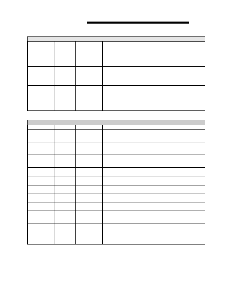
2087
ACC Micro
TM
65
Table 3-9 Keyboard/Mouse Interface
Pin Name
Pin #
Type
Description
ENSDL#
ENKBD
171
I/O
This pin enables the transceiver for SD0-SD7 and D16-D23. When
pulled up, this pin enables the internal keyboard and when pulled
down, this pin disables the internal keyboard.
ENSDH#
M486
172
I/O
This pin enables the transceiver for SD8-SD15 and D24-D31. When
pulled high, this pin is the 486 CPU mode select and when pulled
low, this pin is the 386 CPU mode select.
KBCLK
KBRST#
145
I/O
When internal keyboard is enabled, it works as keyboard controller
clock pin. Otherwise it works as keyboard reset input.
KBDATA
KGA20
144
I/O
When internal keyboard is enabled, it works as keyboard data pin.
Otherwise it works as keyboard GA20 input.
MSCLK
KBINT
143
I/O
When internal keyboard is enabled, it works as mouse clock pin and
the keyboard interrupt is generated by internal keyboard controller.
Otherwise it works as keyboard interrupt input.
MSDATA
IRQ12
142
I/O
When internal keyboard is enabled, it works as mouse data pin and
the mouse interrupt IRQ2 is generated by internal keyboard
controller. Otherwise it works as IRQ12 input.
Table 3-10 FDC Interface
Pin Name
Pin #
Type
Description
X24M
7
I
24MHz input for FDC..
MO0#
DRQ2#
250
I/O
When internal floppy disk is enabled, the MOTOR ON 0 output and
the DRQ2 is generated by internal FDC. Otherwise it is DRQ2
input. (open drain) 24mA.
MO1#
DACK2#
251
O
When internal floppy disk is enabled, the MOTOR ON1 output and
the DACK2# is generated by internal FDC. Otherwise is is
DACK2# output. (Open drain) 24mA.
DS0
IRQ6
247
I/O
When internal floppy disk enable, it works as disk select 0 output and
the IRQ6 is generated by internal FDC. Otherwise it works as IRQ6
input. Open drain (24mA)
DS1
ENFDC
249
I/O
Pull high to enable internal floppy disk controller. Disk select 1
output. 24mA open drain.
FDCWE#
4
O
Write Enable. When set to 0, causes a write operation to the floppy
disk drive. An open drain output. 24ma.
FDCDIR#
5
O
Direction of the head stepper motor. An open drain output. Logic 1
= outward motion. Logic 0 = inward motion. 24ma.
HEAD#
8
O
Head select. Open drain output. Determines which disk drive head
is active. Logic 1 = Side 0. Logic 0 = Side 1. 24ma.
WRDATA#
252
O
Write Data. Logic low open drain. Writes precompensated serial
data to the selected FDD. An open drain output. 24ma.
STEP#
3
O
STEP# output pulses. Active low open drain output. Produces a
pulse at a programmable rate to move the head to another cylinder.
24ma.
INDEX#
256
I
Active low Schmitt input from the disk drive. Senses the head
positioning over the beginning of a track marked by an index hole.
TTL Schmitt trigger.
TRK0#
255
I
Track 0. Active low Schmitt input from the disk drive. Signals that
the head is positioned over the outermost track. TTL Schmitt trigger.

2087
ACC Micro
TM
66
Table 3-10 FDC Interface contd..
Pin Name
Pin #
Type
Description
WP#
254
I
Write Protected. Active low Schmitt input from the disk
drive indicates that the diskette is write protected. TTL
Schmitt trigger.
RDDATA#
1
I
Read data input. Signals read from the FDD to the
microprocessor. TTL Schmitt trigger.
DSKCHG#
253
I
Diskette change. This signal is active low at power-on and
when the diskette is removed. It remains active until a
STEP# pulse is received with the diskette in place.
RWC#
2
O
Reduced write current. 24ma.
1:
500KB
0:
250, 300KB
Table 3-11 COM1 Interface
Pin Name
Pin #
Type
Description
TX1
IRQ4
ENCOM1
245
I/O
Pull high to enable internal COM1 otherwise it will disable
internal COM1. When enable, it works as serial data out and
IRQ4 is generated by internal COM1. Otherwise it works as
IRQ4 input.
DTR1#
244
O
Data Terminal Ready. 4ma.
RTS1#
243
O
Request to Send. 4ma.
RX1
242
I
Serial Data In.
CTS1#
24
I
Clear to Send.
DSR1#
23
I
Data Set Ready.
DCD1#
22
I
Data Carrier Detected.
RI1#
246
I
Ring Indicator.
Table 3-12 COM2 Interface
Pin Name
Pin #
Type
Description
TX2
IRQ3
ENCOM2
10
I/O
Pull high to enable internal COM2. Serial data out and IRQ3
is generated by internal COM2. Otherwise it works as IRQ3
input.
DTR2#
ENLPT
11
O
Pull high to enable parallel port. Data Terminal Ready.
RTS2#
ENIDE
12
O
Pull high to enable internal IDE. Otherwise it works as
Request to Send. 4ma.
RX2
13
I
Serial Data In.
CTS2#
14
I
Clear to Send.
DSR2#
15
I
Data Set Ready.
DCD2#
16
I
Data Carrier Detected.
RI2#
9
I
Ring Indicator.

2087
ACC Micro
TM
67
Table 3-13 IDE and LPT1 Interface
Pin Name
Pin #
Type
Description
ID7
231
I/O
IDE Data Bus bit 7. 12 ma.
STB#
233
I/O
Parallel port Strobe. 12 ma.
ATFD#
235
I/O
Parallel port Autofeed. 12 ma.
INIT#
236
I/O
Parallel port Initialize. 12 ma.
SLIN#
232
I/O
Parallel port Select. 12 ma.
LPTERR#
29
I
Parallel port Error.
LPTBZY
25
I
Parallel port Busy.
SLCT
26
I
Parallel port Selected.
PE
27
I
Parallel port End of Paper.
LPTACK#
28
I
Parallel port Acknowledge Signal from printer
PD0-PD7
18-21
237,
239-241
I/O
Parallel port data bus. 12 ma.

2087
ACC Micro
TM
68
3.2
2087 Numerical Pin List
Pin #
Pin Name
Pin #
Pin Name
Pin #
Pin Name
Pin #
Pin Name
1
RDDATA#
61
A4
121
GND
181
SD5
2
RWC#
62
A5
122
RAS2#
182
SD6
3
STEP#
63
A6
123
VCC
183
VCC
4
FDCWE#
64
A7
124
RAS3#
184
SD7
5
FDCIR#
65
A8
125
STPCLK#
185
SD8
6
GND
66
A9
126
SMI#
186
GND
7
X24M
67
A10
127
LBA#
187
SD9
8
HEAD#
68
A11
128
HLDA
188
SD10
9
R12#
69
GND
129
MASTER#
189
SD11
10
TX2
70
CLKSRC
130
EXTSMI1
190
SD12
11
DTR2#
71
VCC
131
IOCHRDY
191
SD13
12
RTS2#
72
A12
132
SA0
192
SD14
13
RX2
73
A13
133
SA1
193
VCC
14
CTS2#
74
ADS#
134
SMIACT#
194
GND
15
DSR2#
75
NPERR
135
IOCS16#
195
SD15
16
DCD2#
76
NPEREQ
136
MEMCS16#
196
SDDIR#
17
VCC
77
PWRGD
137
EXTSMI0
197
XDIR#
18
PD0
78
A14
138
SRBTN#
198
IOR#
19
PD1
79
A15
139
ZWS#
199
IOW#
20
PD2
80
A16
140
GND
200
BALE
21
PD3
81
A17
141
X14M
201
AEN
22
DCD1#
82
A18
142
MSDATA
202
DRQ0
23
DSR1#
83
A19
143
MSCLK
203
PWRCTL4
24
CTS1#
84
A20
144
KBDATA
204
PWRCTL5
25
LPTBZY
85
A21
145
KBCLK
205
DRQ5
26
SLCT
86
A22
146
VCC
206
PWRCTL6
27
PE
87
A23
147
ENMAX#
207
PWRCTL7
28
LPTACK#
88
A24
148
DAC0
208
SBHE#
29
LPTERR#
89
A25
149
DAC1
209
MEMR#
30
CPURST
90
A31
150
PWRCNTL3
210
GND
31
ENABUS#
91
GND
151
ACPWR
211
VCC
32
NMI
92
GA20
152
ALARM
212
MEMW#
33
GND
93
HITM#
153
D0
213
RESETDRV
34
SYSCLK
94
BE0#
154
D1
214
REF#
35
PHOLD
95
BE1#
155
D2
215
SMEMR#
36
KEN#
96
BE2#
156
D3
216
SMEMW#
37
RDY#
97
BE3#
157
D4
217
TC
38
DTYWE#
98
LA20
158
D5
218
RTCAS
39
CPUBZY#
99
WEN#
159
D6
219
IRQ5
40
INTR
100
VCC
160
D7
220
IRQ7
41
M/-IO
101
MA0, TAG0
161
D8
221
RTCINT#
42
D/-C
102
MA1, TAG1
162
D9
222
IRQ9
43
W/-R
103
MA2,TAG2
163
GND
223
IRQ10
44
BRDY#
104
GND
164
D10
224
IRQ11
45
TGLA2
105
MA3, TAG3
165
D11
225
STPGNT#
46
TGLA3
106
MA4, TAG4
166
D12
226
IRQ14
47
VCC
107
MA5, TAG5
167
D13
227
SUSPMOD#
48
CLKI
108
MA6, TAG6
168
D14
228
SUSPACK#
49
CLKX2
109
MA7, TAG7
169
D15
229
SPEAKER
50
GND
110
MA8, TAG8
170
VCC
230
GND
51
CLKX1
111
GND
171
ENSDL#
231
ID7
52
PWRCTL2
112
VCC
172
ENSDH#
232
SLIN#
53
MDIR#
113
TMA9, TAG9
173
LBAT#
233
STB#
54
KRMOE#
114
DIRTY
174
EXTSYS#
234
GND
55
KRMWE#
115
CAS0#
175
SD0
235
ATFD#
56
PWRCTL1
116
CAS1#
176
SD1
236
INIT#
57
PWRCTL0
117
CAS2#
177
SD2
237
PD4
58
KTGOE#
118
CAS3#
178
GND
238
VCC
59
A2
119
RAS0#
179
SD3
239
PD5
60
A3
120
RAS1#
180
SD4
240
PD6

2087
ACC Micro
TM
69
2087 Numerical Pin List contd...
Pin #
Pin Name
Pin #
Pin Name
Pin #
Pin Name
Pin #
Pin Name
241
PD7
245
TX1
249
DS1
253
DSKCHG#
242
RX1
246
RI1#
250
MO0#
254
WP#
243
RTS1#
247
DS0
251
MO1#
255
TRK0#
244
DTR1#
248
GND
252
WRDATA#
256
INDEX#
3.3
2087 Desktop vs. Notebook Multiplexed Pin Summary
Note:
Notebook Mode : During power on, a pull-down on DAC0 and a pull-up on DAC1 will configure the
ACC2086 to notebook mode.
Desktop Mode : During power on, a pull-down on both DAC0 and DAC1 will configure the
ACC2086 to
desktop mode.
DAC0 = 0
DAC1 = 0
DAC0 = 0
DAC1 = 1
PAR0
AC POWER
PAR2
BAT LOW
PAR3
EXT SYS
KWE EVEN
KWE
KOE EVEN
KOE
KWE ODD
PWRCTL0
KOE ODD
PWRCTL1
KA3 EVEN
KA3
KA3 ODD
KA2
MD LATCH
PWRCTL2
IRQ13
STOP GNT
IRQ15
SUSPEND
DAC0
DACK0
DAC1
DACK5
DAC2
PWRCTL3
DRQ1
PWRCTL4
DRQ3
PWRCTL5
DRQ6
PWRCTL6
DRQ7
PWRCTL7
IO CHK
EXTSMI1
3.4
2087 Pins Status For Various CPU Types
Note: The ACC 2087 supports level 1 write back and write through microprocessors.
Pin 58 (KTGOE)
Pin 147 (ENMAX#)
ROM
CPU Type
Pull down (0)
Pull down (0)
8 bit
P24D (Misc.)
Pull down (0)
Pull up (1)
8 bit
other write back
Pull up (1)
Pull down (0)
16 bit
Regular CPU
Pull up (1)
Pull up (1)
8 bit
Regular CPU

2087
ACC Micro
TM
70
3.5
2087 Numerical Pin List with Multiplexed pins and Power Plane Summary
Pin #
Voltage
Pin Name
Pin #
Voltage
Pin Name
Pin #
Voltage
Pin Name
1
5 V
RDDATA#
61
3.3 V
A4
121
3.3 V
GND
2
5 V
RWC#
62
3.3 V
A5
122
3.3 V
RAS2#
3
5 V
STEP#
63
3.3 V
A6
123
3.3 V
VCC
4
5 V
FDCWE#
64
3.3 V
A7
124
3.3 V
RAS3#
5
5 V
FDCIR#
65
3.3 V
A8
125
3.3 V
STPCLK#
6
5 V
GND
66
3.3 V
A9
126
3.3 V
SMI#
7
5 V
X24M
67
3.3 V
A10
127
3.3 V
LBA#,
READY0#
8
5 V
HEAD#
68
3.3 V
A11
128
3.3 V
HLDA
9
5 V
R12#
69
3.3 V
GND
129
5 V
MASTER#
10
5 V
TX2, IRQ3,
ENCOM2
70
3.3 V
CLKSRC
130
5 V
EXTSMI1,
IOCHK
11
5 V
DTR2#, ENLPT
71
5 V
VCC
131
5 V
IOCHRDY
12
5 V
RTS2#, ENIDE
72
3.3 V
A12
132
5 V
SA0
13
5 V
RX2
73
3.3 V
A13
133
5 V
SA1
14
5 V
CTS2#
74
3.3 V
ADS#
134
5 V
SMIACT#,
SMIADS#
15
5 V
DSR2#
75
3.3 V
NPERR
135
5 V
IOCS16#
16
5 V
DCD2#
76
3.3 V
NPEREQ,
BLAST#
136
5V
MEMCS16#
17
5 V
VCC
77
3.3 V
PWRGD
137
5 V
EXTSMI0
18
5 V
PD0
78
3.3 V
A14
138
5 V
SRBTN#
19
5 V
PD1
79
3.3 V
A15
139
5 V
ZWS#
20
5 V
PD2
80
3.3 V
A16
140
5V
GND
21
5 V
PD3
81
3.3 V
A17
141
5 V
X14M
22
5 V
DCD1#
82
3.3 V
A18
142
5 V
MSDATA,
IRQ12
23
5 V
DSR1#
83
3.3 V
A19
143
5 V
MSCLK,
KBINT
24
5 V
CTS1#
84
3.3 V
A20
144
5 V
KBDATA,
KGA20
25
5V
LPTBZY
85
3.3 V
A21
145
5 V
KBCLK,
KBRST#
26
5 V
SLCT
86
3.3 V
A22
146
5V
VCC
27
5 V
PE
87
3.3 V
A23
147
5 V
ENMAX#
28
5 V
LPTACK#
88
3.3 V
A24
148
5 V
DAC0, DACK0
29
5V
LPTERR#
89
3.3 V
A25
149
5 V
DAC1, DACK5
30
3.3 V
CPURST
90
3.3 V
A31
150
5V
PWRCNTL3,
DAC2

2087
ACC Micro
TM
71
2087 Numerical Pin List with Multiplexed pins and Power Plane Summary contd...
Pin #
Voltage
Pin Name
Pin #
Voltage
Pin Name
Pin #
Voltage
Pin Name
31
3.3 V
ENABUS#
91
3.3 V
GND
151
3.3 V
ACPWR, PAR0
32
3.3 V
NMI
92
3.3 V
GA20
152
3.3 V
ALARM, PAR1
33
3.3 V
GND
93
3.3 V
HITM#,
FLUSH#
153
3.3 V
D0
34
3.3 V
SYSCLK
94
3.3 V
BE0#
154
3.3 V
D1
35
3.3 V
PHOLD
95
3.3 V
BE1#
155
3.3 V
D2
36
3.3 V
KEN#
96
3.3 V
BE2#
156
3.3 V
D3
37
3.3 V
RDY#
97
3.3 V
BE3#
157
3.3 V
D4
38
3.3 V
DTYWE#, NA#
KTWE#
98
3.3 V
LA20, EADS#
158
3.3 V
D5
39
3.3 V
CPUBZY#,
IGNNE#
99
3.3 V
WEN#
159
3.3 V
D6
40
3.3 V
INTR
100
3.3 V
VCC
160
3.3 V
D7
41
3.3 V
M/-IO
101
3.3 V
MA0, TAG0,
ROMCS#
161
3.3 V
D8
42
3.3 V
D/-C
102
3.3 V
MA1, TAG1,
CS8042#
162
3.3 V
D9
43
3.3 V
W/-R
103
3.3 V
MA2,TAG2,
RTCDS#
163
3.3 V
GND
44
3.3 V
BRDY#,
CPUPEREQ
104
3.3 V
GND
164
3.3 V
D10
45
3.3 V
TGLA2
105
3.3 V
MA3, TAG3,
RTCWR#
165
3.3 V
D11
46
3.3 V
TGLA3
106
3.3 V
MA4, TAG4,
HCS0#
166
3.3 V
D12
47
3.3 V
VCC
107
3.3 V
MA5, TAG5,
HCS1#
167
3.3 V
D13
48
3.3 V
CLKI
108
3.3 V
MA6, TAG6,
IENH#
168
3.3 V
D14
49
3.3 V
CLKX2
109
3.3 V
MA7, TAG7,
IENL#
169
3.3 V
D15
50
3.3 V
GND
110
3.3 V
MA8, TAG8
170
3.3 V
VCC
51
3.3 V
CLKX1
111
3.3 V
GND
171
3.3 V
ENSDL#,
ENKBD
52
3.3 V
PWRCTL2,
MDLATCH
112
3.3 V
VCC
172
3.3 V
ENSDH#,
M486
53
3.3 V
MDIR#
113
3.3 V
MA9, TAG9
RDIDX21#
173
3.3 V
LBAT#, PAR2
54
3.3 V
KRMOE#
114
3.3 V
DIRTY, MA10
174
3.3 V
EXTSYS#,
PAR3
55
3.3 V
KRMWE#
115
3.3 V
CAS0#
175
5 V
SD0
56
3.3 V
PWRCTL1,
KOEB
116
3.3 V
CAS1#
176
5 V
SD1
57
3.3 V
PWRCTL0,
KWEB
117
3.3 V
CAS2#
177
5 V
SD2
58
3.3 V
KTGOE#
118
3.3 V
CAS3#
178
5 V
GND
59
3.3 V
A2
119
3.3 V
RAS0#
179
5 V
SD3
60
3.3 V
A3
120
3.3 V
RAS1#
180
5 V
SD4

2087
ACC Micro
TM
72
2087 Numerical Pin List with Multiplexed pins and Power Plane Summary contd...
Pin #
Voltage
Pin Name
Pin #
Voltage
Pin Name
Pin #
Voltage
Pin Name
181
5 V
SD5
206
5 V
PWRCTL6,
DRQ6
231
5 V
ID7
182
5 V
SD6
207
5 V
PWRCTL7,
DRQ7
232
5 V
SLIN#
183
5 V
VCC
208
5 V
SBHE#
233
5 V
STB#
184
5 V
SD7
209
5 V
MEMR#
234
5 V
GND
185
5 V
SD8
210
5 V
GND
235
5 V
ATFD#
186
5 V
GND
211
5 V
VCC
236
5 V
INIT#
187
5 V
SD9
212
5 V
MEMW#
237
5 V
PD4
188
5 V
SD10
213
5 V
RESETDRV
238
5 V
VCC
189
5 V
SD11
214
5 V
REF#
239
5 V
PD5
190
5 V
SD12
215
5 V
SMEMR#
240
5 V
PD6
191
5 V
SD13
216
5 V
SMEMW#
241
5 V
PD7
192
5 V
SD14
217
5 V
TC
242
5 V
RX1
193
5 V
VCC
218
5 V
RTCAS
243
5 V
RTS1#
194
5 V
GND
219
5 V
IRQ5
244
5 V
DTR1#
195
5 V
SD15
220
5 V
IRQ7
245
5 V
TX1, IRQ4,
ENCOM1
196
5 V
SDDIR#
221
5 V
RTCINT#
246
5 V
RI1#
197
5 V
XDIR#
222
5 V
IRQ9
247
5 V
DS0, IRQ6
198
5 V
IOR#
223
5 V
IRQ10
248
5 V
GND
199
5 V
IOW#
224
5 V
IRQ11
249
5 V
DS1, ENFDC
200
5 V
BALE
225
5 V
STPGNT#,
IRQ13
250
5 V
MO0#, DRQ2#
201
5 V
AEN
226
5 V
IRQ14
251
5 V
MO1#, DACK2
202
5 V
DRQ0
227
5 V
SUSPMOD#,
IRQ15
252
5 V
WRDATA#
203
5 V
PWRCTL4,
DRQ1
228
5 V
SUSPACK#
253
5 V
DSKCHG#
204
5 V
PWRCTL5,
DRQ3
229
5 V
SPEAKER
254
5 V
WP#
205
5 V
DRQ5
230
5 V
GND
255
5 V
TRK0#
256
5 V
INDEX#
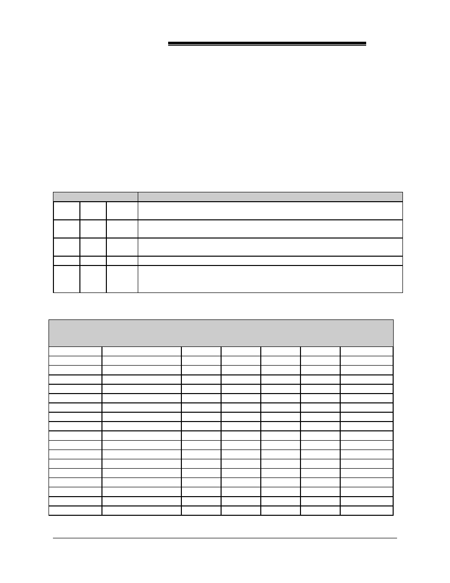
2087
ACC Micro
TM
73
Section 4
4.1 ACC2087 Register Settings
The configuration registers in the ACC2087 are programmed with an indirect addressing scheme using I/O
adddresses F2 and F3. I/O address F2 contains the write/read configuration index register. F2 selects the
corresponding configuration register accessed at I/O address F2. To write a value of "E8" into configuration
register 2Ah, the configuration index register at I/O address F2 must first be written with a value ao "2a," then
register at I/O address F3 with a value of :E8."
All reserved and unused bits should be written as zero unless otherwise indicated as one or x (don't care).
Memory Configuration and ROM Setup - Register 0h
Bit
R/W
Default
Function
7-5
R/W
0
When set to one this bit enables remap memory within the 640 KB to 1 MB range
to memory address above the actual installed memory size.
6
R/W
0
When set to zero ROM BIOS will be located in 0F0000-0FFFFF. When set to one
ROM BIOS will be extended from 0E0000-0FFFFF.
5
R/W
0
When set to zero ROM BIOS will be located in 0F0000-0FFFFF. When set to one
ROM BIOS will be extended from 0E0000-0FFFFF.
4
R/W
0
When set to one this bit enables ROM to include C0000-C7FFF for video BIOS.
3-0
R/W
0
These bits are memory configuration bits 3-0. These four bits plus bits 1 and 0 of
Register 12h, set the memory option. Refer to the following table for memory
options.
Memory Options
Option
Memory
Configuration
5 4 3 2 1 0
Bank 0
Bank 1
Bank 2
Bank 3
Total
Memory
1
0 0 0 0 0 0
256K
1M
2
0 0 0 1 0 0
256K
256K
2M
3
0 0 0 1 1 1
256K
256K
256K
3M
4
0 0 1 0 0 1
256K
256K
256K
256K
4M
5
0 1 0 0 0 0
1M
4M
6
0 1 0 0 0 1
256K
1M
5M
7
0 1 0 0 1 0
256K
256K
1M
6M
8
0 1 0 0 1 1
256K
256K
256K
1M
7M
9
0 1 0 1 0 0
1M
1M
8M
10
0 1 0 1 0 1
256K
1M
1M
9M
11
0 1 0 1 1 0
256K
256K
1M
1M
10M
12
0 1 0 1 1 1
1M
1M
1M
12M
13
0 1 1 0 0 0
256K
1M
1M
1M
13M
14
0 1 1 0 0 1
1M
1M
1M
1M
16M
15
1 0 0 0 0 0
4M
16M
16
1 0 0 0 0 1
1M
4M
20M
17
1 0 0 0 1 0
1M
1M
4M
24M
18
1 0 0 0 1 1
1M
1M
1M
4M
28M
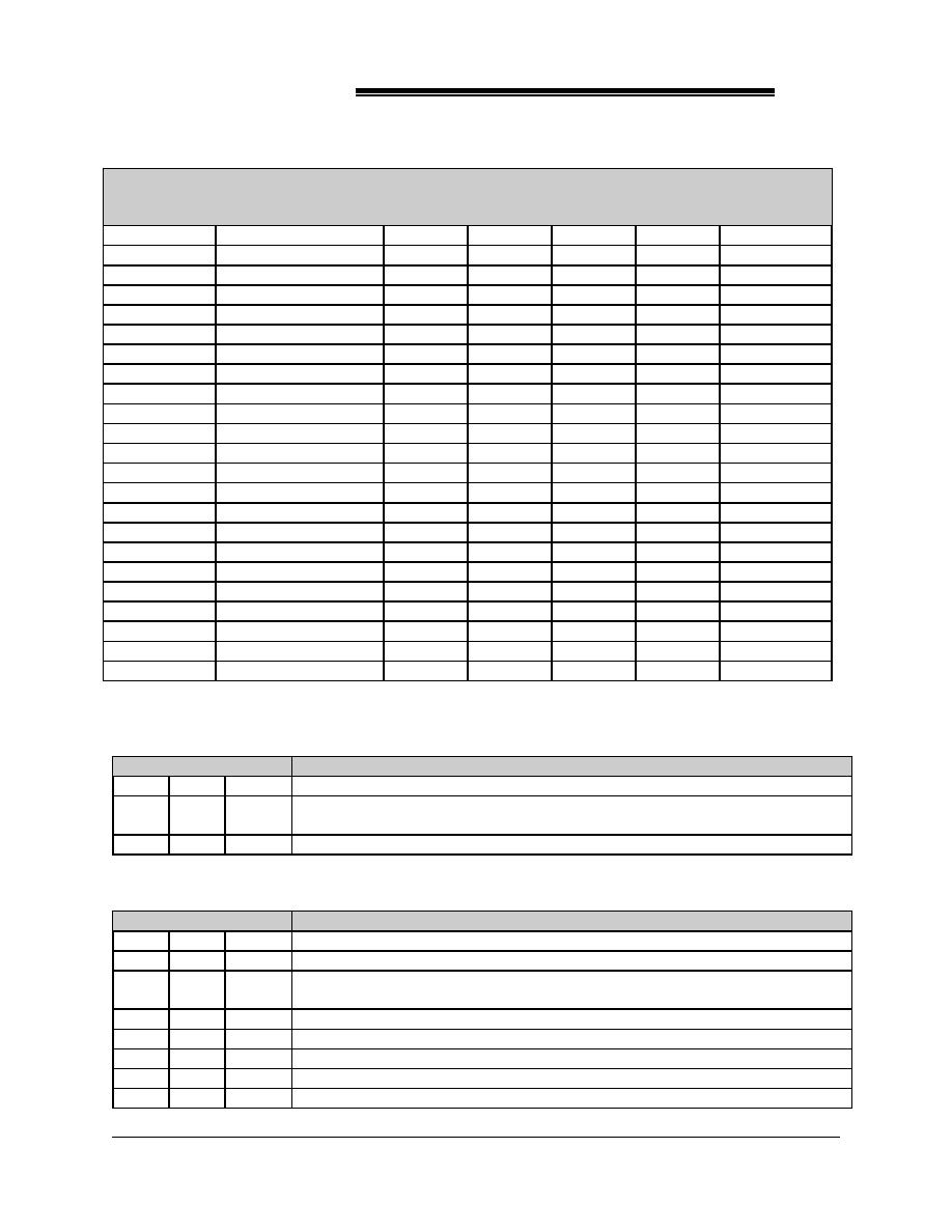
2087
ACC Micro
TM
74
Memory Options continued...
Option
Memory
Configuration
5 4 3 2 1 0
Bank 0
Bank 1
Bank 2
Bank 3
Total
Memory
19
1 0 0 1 0 0
4M
4M
32M
20
1 0 0 1 0 1
1M
4M
4M
36M
21
1 0 0 1 1 0
1M
1M
4M
4M
40M
22
1 0 0 1 1 1
4M
4M
4M
48M
23
1 0 1 0 0 0
1M
4M
4M
4M
52M
24
1 0 1 0 0 1
4M
4M
4M
4M
64M
25
1 1 0 0 0 0
512K
2M
26
1 1 0 0 0 1
512K
512K
4M
27
1 1 0 0 1 0
512K
512K
512K
6M
28
1 1 0 0 1 1
512K
512K
512K
512K
8M
29
1 1 0 1 0 0
512K
1M
6M
30
1 1 0 1 0 1
512K
512K
1M
8M
31
1 1 0 1 1 0
512K
512K
1M
1M
12M
32
1 1 0 1 1 1
512K
4M
18M
33
1 1 1 0 0 0
512K
512K
4M
20M
34
1 1 1 0 0 1
512K
512K
4M
4M
36M
35
0 0 0 0 1 0
256K
256K
4M
18M
36
0 0 0 1 1 0
256K
256K
4M
4M
34M
37
0 0 0 0 0 1
256K
4M
17M
38
1 1 1 1 0 0
2M
8M
39
1 1 1 1 0 1
2M
2M
16M
40
1 1 1 1 1 0
2M
1M
12M
41
1 1 1 1 1 1
2M
4M
24M
* Memory configuration bits 5 and 4 are located in Register 12h, bits 1 and 0.
FP Dram Setup - Register 1h
Bit
R/W
Default
Function
7-5
R
x
Reserved.
4
R/W
0
When set to one this bit disables RAS time out. When set to zero this bit enables
RAS time out.
3-0
R
x
Reserved.
Shadow RAM Setup - Register 2h
Bit
R/W
Default
Function
7
R/W
1
This bit must be set to one.
6
R/W
0
When set to one this bit enables shadow area to be cacheable.
5
R/W
0
When set to one this bit places the shadow segment into read only, write protect
mode.
4
R/W
0
When set to one this bit enables shadow segment F0000-FFFFF.
3
R/W
0
When set to one this bit enables shadow segment E0000-EFFFF.
2
R/W
0
When set to one this bit enables shadow segment D0000-DFFFF.
1
R/W
0
When set to one this bit enables shadow segment C8000-CFFFF.
0
R/W
0
When set to one this bit enables shadow segment C0000-C7FFF.
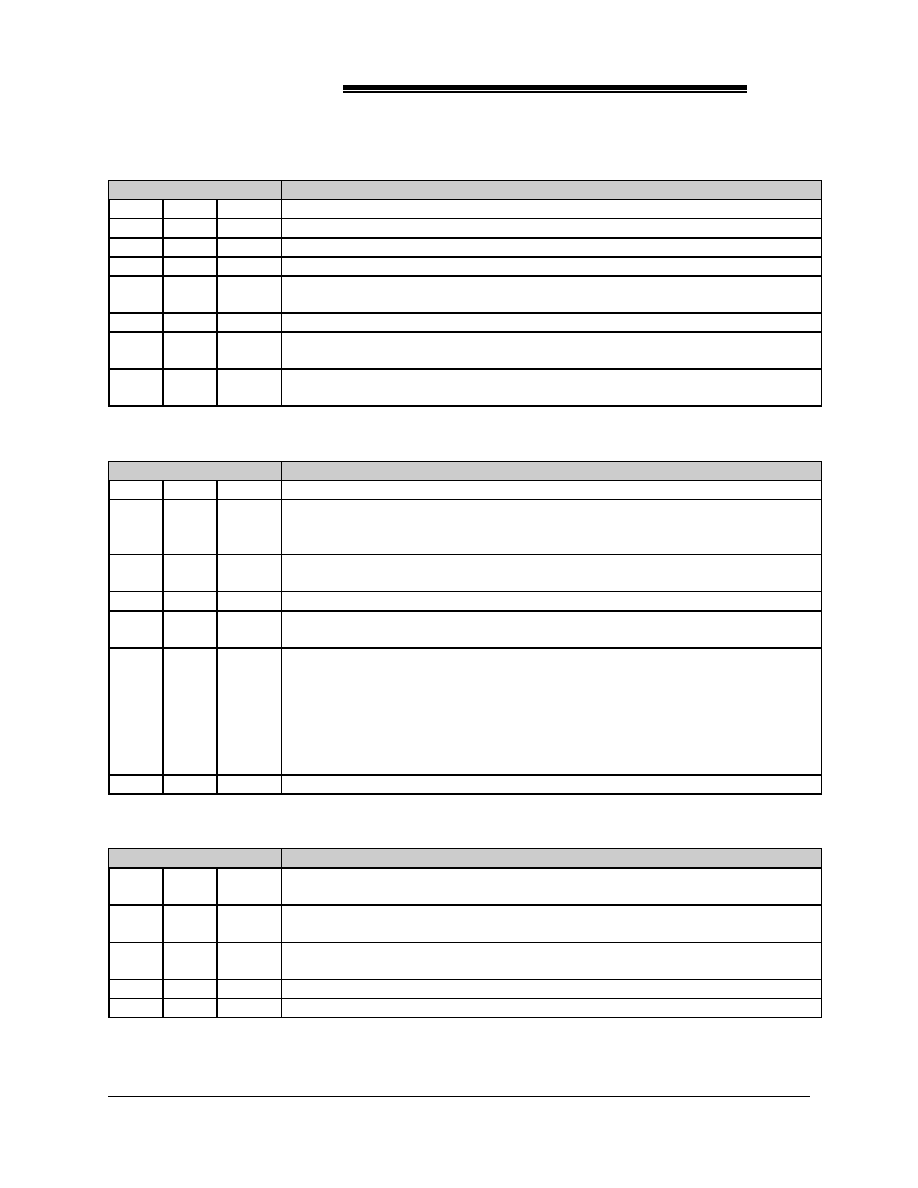
2087
ACC Micro
TM
75
DRAM, Coprocessor and Parity Setup - Register 3h
Bit
R/W
Default
Function
7
R
x
Reserved.
6
R/W
0
When set to one this bit enables CAS before RAS AT refresh.
5
R
x
Reserved.
4
R/W
When set to one this bit disables parity check.
3
R/W
0
When set to one the numeric processor operates in 1 wait state. When set to zero
the numeric processor operates in 2 wait states.
2
R/W
0
When set to one this bit disables the numeric processor's sequencer.
1
R/W
0
When set to one this bit disables access to the Weitek 3167 coprocessor. All
access to Weitek will become AT Bus cycles.
0
R/W
0
When set to one this bit disables access to the 387 processor. All access to 387
will become AT Bus cycles.
Cache Setup - Register 4h
Bit
R/W
Default
Function
7
R/W
0
When set to one this bit enables post write.
6
R/W
0
When set to one this bit enables memory write 0 wait for 486 with no cache
operation in page hit cycle. When set to zero this bit enables memory write 1 wait
for 486 with no cache operation in page hit cycle.
5
R/W
0
When set to one this bit enables cache read 1 wait state. When set to zero this bit
enables cache read zero wait state.
4
R/W
0
When set to one this bit enables DRAM read burst mode.
3
R/W
0
When set to one this bit enables cache read burst mode to update the 486 internal
cache.
2,1
R/W
0
These two bits set the cache line size as follows:
Bit
Line Size
2 1
0 0
32
1 0
32
0 1
64
1 1
128
0
R/W
0
When set to one this bit enables the 2087 cache controller.
Power Up Select and Slow Refresh - Register 5h
Bit
R/W
Default
Function
7
R
0
This is a read only bit. When read as one, this bit indicates an 8-bit ROM is
installed. When read as zero, this bit indicates a 16-bit ROM is installed.
6
R
0
This is a read only bit. When read as one, it indicates 386 mode is selected. When
read as zero, it indicates 486 mode is selected.
5
R
0
This is a read only bit. When read as zero it indicates Level 1 write through CPU.
When read as one it indicates Lever 1 write back CPU.
4
R
x
Reserved.
3
R/W
0
When set to one this bit enables F3 to be read from the SD instead of XD.

2087
ACC Micro
TM
76
Power Up Select and Slow Refresh - Register 5h
Bit
R/W
Default
Function
2
R
x
Reserved.
1-0
R/W
1
Bits 1 and 0 select the slow refresh divisor (Read/Write) as follows:
Bits
Divided by
1 0
0 0
1 (Default)
0 1
2
1 0
4
1 1
8
These bits must be set to one.
AT Bus Clock Source Select - Register 6h
Bit
R/W
Default
Function
7-5
R/W
0
When Reg. 1Ah bit 0 is 1, these bits select the divisor from CLKSRC for the
digital delay time.
Bits
7 6 5 DMA Clock Source
0 0 0 3 (Default)
0 0 1 5
0 1 0 1.5
0 1 1 2.5
1 0 0 1
1 0 1 1
1 1 0 2
1 1 1 4
4-0
R
0
Select clock source for AT Bus clock. The 2087 supports three clock sources for
the AT Bus clock. SYSCLK is half of the AT bus clock. When bit 4 is set at zero
(default), the SYSCLK is derived from X14M1 (14.318 MHz). When bits 4 and 3
are set at one, the SYSCLK is derived from X24M (24 MHz). When bit 4 is one
and bit 3 is zero, CLKSRC provides the clock source. In addition, bits 2-0 set a
divisor to divide down CLKSRC for the use of SYSCLK.
Bits
4 3 2 1 0
AT Bus clock source
0 X X X X
X14M1, default.
1 1 X X X
X24M
1 0 0 0 0
CLKSRC/5
1 0 0 0 1
CLKSRC/3
1 0 0 1 0
CLKSRC/2.5
1 0 0 1 1
CLKSRC/1.5
1 0 1 0 0
CLKSRC/1
1 0 1 0 1
CLKSRC/4
1 0 1 1 0
CLKSRC/1
1 0 1 1 1
CLKSRC/2

2087
ACC Micro
TM
77
Sleep Mode Control - Register 8h
Bit
R/W
Default
Function
7-4
R
x
Reserved.
3
R/W
0
When set to one this bit enables sleep mode. If sleep mode is enabled, the system
clock source will be switched from CLKSRC to AT bus clock which is divided
down to a sleep mode frequency.
2-0
R/W
0
These bits select the divisor to divide the AT bus clock source to the sleep mode
clock.
Bits
Divisor Sleep
2 1 0
Mode
Clock
0 0 0 1 (Default)16 MHz
0 0 1
32
0.5 MHz
0 1 0
64
0.25MHz
0 1 1
128
0.125 MHz
1 0 0
2
8 MHz
1 0 1
4
4 MHz
1 1 0
8
2 MHz
1 1 1
16
1 MHz
Non-cacheable range and DRAM setup - Register 9h
Bit
R/W
Default
Function
7-4
R/W
0
Bit 7
Bit 6
Bit 5
Bit 4 Non-cacheable range
0
0
0
0
default
1
0
0
0
address>32Mb
1
1
0 0
address>16Mb
1
1
1
0
address>8Mb
1
1
1
1
address>4Mb
3-2
R
x
Reserved.
1
R/W
0
When set to one this bit enables 512K base memory. Default is zero (640K base
memory).
0
R
x
Reserved.
DMA High Address 24, 25 Register 0Ah
Bit
R/W
Default
Function
7
R/W
0
When set to one this bit will convert ROMOE to ROMCS for flash EPROM
support.
6
R/W
0
When this bit is set to one EADS# is synchronized with CPU clock and activated
for only one CPU Clock period for Level 1 write through CPU.
5
R/W
0
When set to zero this bit disables KEN (KEN is always deasserted) in 486 normal
operation.
4
R
0
Reserved. Set to zero
3
R
1
Reserved. Must be set to one.

2087
ACC Micro
TM
78
DMA High Address 24, 25 Register 0Ah
Bit
R/W
Default
Function
2
R/W
0
When set to one MA latches will be held until the last half clock of CAS to
increase the MA to CAS hold time.
1
R/W
0
When set to one this bit enables the address bit 24 for non CPU cycle.
0
R/W
0
When set to one this bit enables the address bit 24 for non CPU cycle.
Page Mode Setup Register 0Bh
Bit
R/W
Default
Function
7-6
R/W
2T
Set RAS precharge time.
Bits
RAS precharge time
7 6
0 0
2T
0 1
3T
1 0
4T
1 1
5T
5
R/W
0
When this bit is set to one the RAS to CAS delay is 3 cycles in write cycle. When
set to zero the RAS to CAS delay time is 2 cycles .
4
R/W
0
When this bit is set to one the CAS precharge time is 2 cycles in write cycles.
When set to zero the CAS precharge time is one cycle.
3-2
R/W
1T
These two bits define CAS width for read cycle time.
Bits
CAS width in read cycle
3 2
0 0
1T
0 1
2T
1 0
3T
1 1
4T
1-0
R/W
1T
These two bits define CAS width for write cycle.
Bits
CAS width in write cycle
1 0
0 0
1T
0 1
2T
1 0
3T
1 1
4T
Non-cacheable Range (Registers 0Ch-11h)
Non-cacheable block 1 Register 0Ch
Bit
R/W
Default
Function
7
R/W
0
When set to one this bit enables non-cacheable block 1 address A17.
6
R/W
0
When set to one this bit enables non-cacheable block 1 address A16.
5
R/W
0
When set to one this bit enables non-cacheable block 1 address A15.

2087
ACC Micro
TM
79
Non-cacheable block 1 Register 0Ch
Bit
R/W
Default
Function
4
R/W
0
When set to one this bit enables non-cacheable block 1 address A14.
3-0
R/W
0
These bits enable set non-cacheable block 1 size as follows:
Non-cacheable Block 1 size select
Bits
Addr. Non-cacheable
compared block size
3210
0000
don't care all cacheable (default)
0001
14-25
16K
0010
15-25
32K
0011
16-25
64K
0100
17-25
128K
0101
18-25
256K
0110
19-25
512K
0111
20-25
1M
1000
21-25
2M
1001
22-25
4M
1010
23-25
8M
1011
24-25
16M
1100
25
32M
1101 - 1111
disable cache
Non-cacheable block 1 Register 0Dh
Bit
R/W
Default
Function
7
R/W
0
When set to one this bit enables non-cacheable block 1address A25.
6
R/W
0
When set to one this bit enables non-cacheable block 1 address A24.
5
R/W
0
When set to one this bit enables non-cacheable block 1 address A23.
4
R/W
0
When set to one this bit enables non-cacheable block 1 address A22.
3
R/W
0
When set to one this bit enables non-cacheable block 1 address A21.
2
R/W
0
When set to one this bit enables non-cacheable block 1 address A20.
1
R/W
0
When set to one this bit enables non-cacheable block 1 address A19.
0
R/W
0
When set to one this bit enables non-cacheable block 1 address A18.
Non-cacheable block 2 Register 0Eh
Bit
R/W
Default
Function
7
R/W
0
When set to one this bit enables non-cacheable block 2 address A17.
6
R/W
0
When set to one this bit enables non-cacheable block 2 address A16.
5
R/W
0
When set to one this bit enables non-cacheable block 2 address A15.

2087
ACC Micro
TM
80
Non-cacheable block 2 Register 0Eh
Bit
R/W
Default
Function
4
R/W
0
When set to one this bit enables non-cacheable block 2 address A14.
3-0
R/W
0
These bits set non-cacheable block 2 size as follows:
Non-cacheable Block 2 size select
Bits
Addr. Non-cacheable
compared block size
3210
0000
don't care all cacheable (default)
0001
14-25
16K
0010
15-25
32K
0011
16-25
64K
0100
17-25
128K
0101
18-25
256K
0110
19-25
512K
0111
20-25
1M
1000
21-25
2M
1001
22-25
4M
1010
23-25
8M
1011
24-25
16M
1100
25
32M
1101 - 1111
disable cache
Non-cacheable block 3 Register 0Fh
Bit
R/W
Default
Function
7
R/W
0
When set to one this bit enables non-cacheable block 2 address A25.
6
R/W
0
When set to one this bit enables non-cacheable block 2 address A24.
5
R/W
0
When set to one this bit enables non-cacheable block 2 address A23.
4
R/W
0
When set to one this bit enables non-cacheable block 2 address A22.
3
R/W
0
When set to one this bit enables non-cacheable block 2 address A21.
2
R/W
0
When set to one this bit enables non-cacheable block 2 address A20.
1
R/W
0
When set to one this bit enables non-cacheable block 2 address A19.
0
R/W
0
When set to one this bit enables non-cacheable block 2 address A18.

2087
ACC Micro
TM
81
Non-cacheable block 3 Register 10h
Bit
R/W
Default
Function
7
R/W
0
When set to one this bit enables non-cacheable block 3 address A17.
6
R/W
0
When set to one this bit enables non-cacheable block 3 address A16.
5
R/W
0
When set to one this bit enables non-cacheable block 3 address A15.
4
R/W
0
When set to one this bit enables non-cacheable block 3 address A14.
3-0
R/W
0
These bits set non-cacheable block 3 size.
Non-cacheable Block 3 size select
Bits
Addr. Non-cacheable
compared block size
3210
0000
don't care all cacheable (default)
0001
14-25
16K
0010
15-25
32K
0011
16-25
64K
0100
17-25
128K
0101
18-25
256K
0110
19-25
512K
0111
20-25
1M
1000
21-25
2M
1001
22-25
4M
1010
23-25
8M
1011
24-25
16M
1100
25
32M
1101 - 1111
disable cache
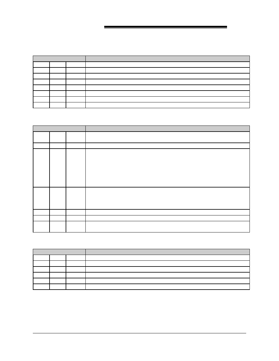
2087
ACC Micro
TM
82
Non-cacheable block 3 Register 11h
Bit
R/W
Default
Function
7
R/W
0
When set to one this bit enables non-cacheable block 3 address A25.
6
R/W
0
When set to one this bit enables non-cacheable block 3 address A24.
5
R/W
0
When set to one this bit enables non-cacheable block 3 address A23.
4
R/W
0
When set to one this bit enables non-cacheable block 3 address A22.
3
R/W
0
When set to one this bit enables non-cacheable block 3 address A21.
2
R/W
0
When set to one this bit enables non-cacheable block 3 address A20.
1
R/W
0
When set to one this bit enables non-cacheable block 3 address A19.
0
R/W
0
When set to one this bit enables non-cacheable block 3 address A18.
DRAM, Rom Size, and Turbo Pin Control - Register 12h
Bit
R/W
Default
Function
7
R/W
0
When set to one the RAS to CAS delay time is 3 cycles for read cycles. When set
to zero the RAS to CAS delay time is 2 cycles.
6
R/W
0
When set to one the CAS precharge time is 2 cycles in read cycle.
5
R/W
0
This bit in conjunction with bit 6, Register 0h sets the ROM size for middle BIOS.
Reg. 12h Reg. 0h
Middle
Bit 5
Bit 6
ROM size
0
0
Disable (default)
0
1
64K (FF0000 - FFFFFF)
1
0
256K (FC0000-FFFFFF)
1
1
512K (F80000-FFFFFF)
4
R/W
0
When set to one this bit enables the Turbo pin (pin 75) to switch the operation
speed between Turbo clock (CLKSRC) and Sleep mode clock (defined by Register
8h, bits 2-0). When set to zero Turbo pin will toggle the operation speed between
Turbo clock (CLKSRC) and Normal clock.
3
R
x
Reserved.
2
R/W
0
When set to one this bit enables 4Mx4 DRAM supported option.
1-0
R/W
0
These two bits are memory configuration bits 5 and 4. Refer to memory
configuration table of Register 0h.
DRAM Bank Relocate Control Register 13h
Bit
R/W
Default
Function
7
R/W
0
SELBNK31
6
R/W
0
SELBNK30
5
R/W
0
SELBNK21
4
R/W
0
SELBNK20
3
R/W
0
SELBNK11
2
R/W
0
SELBNK10

2087
ACC Micro
TM
83
DRAM Bank Relocate Control Register 13h
Bit
R/W
Default
Function
1
R/W
0
SELBNK01
0
R/W
0
SELBNK00
SELBNK01
SELBNK00
RAS0# redirect to bank #
0
0
0 (default)
0
1
1
1
0
2
1
1
3
SELBNK11
SELBNK10
RAS1# redirect to bank #
0
0
1 (default)
0
1
2
1
0
3
1
1
0
SELBNK21
SELBNK20
RAS2# redirect to bank #
0
0
2 (default)
0
1
3
1
0
0
1
1
1
SELBNK31
SELBNK30
RAS3# redirect to bank #
0
0
3 (default)
0
1
0
1
0
1
1
1
2
AT Bus Cycle Control - Register 14h
Bit
R/W
Default
Function
7
R/W
0
When set to one this bit disables BS16# output.
6
R/W
0
When set to one this bit enables cache write hit cycle zero wait state.
5
R
x
Reserved.
4
R/W
0
When set to one this bit enables 8 bit cycle, 0 wait state.
3
R/W
0
When set to one this bit enables 16 bit cycle, 0 wait state.
2-1
R
x
Reserved.
0
R/W
0
When set to one this bit disables AT Bus 32 bit cycle.
AT Bus Control - Register 15h
Bit
R/W
Default
Function
7
R/W
0
When set to one this bit enable AT bus hold time.
6
R/W
0
When set to one this bit enable slow I/O recovery time. Default is zero.
5
R/W
0
16 bit I/O Recovery control bit 2.
4
R/W
0
16 bit I/O Recovery control bit 1.
3
R/W
0
16 bit I/O Recovery control bit 0.

2087
ACC Micro
TM
84
AT Bus Control - Register 15h
Bit
R/W
Default
Function
2
R/W
0
8 bit I/O Recovery control bit 2.
1
R/W
0
8 bit I/O Recovery control bit 1.
0
R/W
0
8 bit I/O Recovery control bit 0.
In 16 bit I/O access
Bit 5
Bit 4
Bit 3
Bit 6=0 Bit 6=1
I/O Recovery time
0
0
0
0
0(default)
0
0
1
1
1
0
1
0
2
5
0
1
1
3
9
1
0
0
4
13
1
0
1
5
17
1
1
0
6
21
1
1
1
7
25
In 8 bit I/O access
Bit 2
Bit 1
Bit 0
Bit 6=0 Bit 6=1
I/O Recovery time
0
0
0
0
0 (default)
0
0
1
1
1
0
1
0
2
5
0
1
1
3
9
1
0
0
4
13
1
0
1
5
17
1
1
0
6
21
1
1
1
7
25
Note: The unit of I/O Recovery time is 8 MHz
cycle.
AT Bus Refresh and DRAM Setup - Register 16h
Bit
R/W
Default
Function
7
R
1
Reserved. Must be set to one.
6
R/W
0
When set to one this bit enables 0 wait ROM cycle.
5-4
R/W
0
These two bits are the AT refresh burst count control bits.
Bit Rate per refresh request
5 4
x 0
1 (Default)
0 1
2
1 1
4
2087
ACC Micro
TM
85
Register 16h
Bit
R/W
Default
Function
3-2
R/W
0
These two bits extend the CAS width for write cycle by activating CAS earlier.
Bit CAS Width Extension
3 2
0 x
No extension. (Default)
1 1
1/2 cycle earlier
1-0
R/W
0
These two bits extend the CAS width for read cycle by activating CAS earlier.
Bit
CAS Width Extension
1 0
0 x
No extension. (Default)
1 1
1/2 cycle earlier
Suspend Mode Control - Register 17h
Bit
R/W
Default
Function
7-3
R
x
Reserved.
2
R
0
Reserved. Must be set to zero.
1
R/W
0
When set to one this bit forces the data level to one and drives data out during 5-
Volt Suspend mode.
0
R
0
Reserved.
L2 , DRAM, and ISA Control - Register 18h
Bit
R/W
Default
Function
7
R/W
0
When set to one this bit enables X-2-2-2 cache read burst cycle.
6
R/W
0
When set to one this bit adds one extra wait state for ISA cycle.
5
R/W
0
When set to one this bit adds one wait state for DRAM and ISA off cycles.
4
R/W
0
If Level 2 write back is implemented cache write wait state will be set to one. If
Level 2 write through is implemented post write wait state will be set to one.
3
R
x
Reserved.
2
R
x
Reserved.
1
R/W
0
When set to one this bit enables hidden burst refresh.
0
R/W
0
When set to one this bit disables AT standard refresh.

2087
ACC Micro
TM
86
DRAM Setup - Register 19h
Bit
R/W
Default
Function
7-6
R/W
0
These two bits define the burst refresh RAS active cycle width. Default is 4T.
Bits
Cycle width
7 6
0 0
5T
0 1
4T
1 0
3T
1 1
2T
5-4
R/W
0
These two bits define the burst refresh RAS precharge cycle width. Default is 4T.
Bits
Cycle width
5 4
0 0
4T
0 1
3T
1 0
2T
1 1
1T
3
R
0
Reserved.
2-0
R/W
0
These three bits define the burst refresh count. Default is 1.
Bits
Burst number
2 1 0
0 0 0
1
0 0 1
2
0 1 0
3
0 1 1
4
1 0 0
5
1 0 1
6
1 1 0
7
1 1 1
8
ADS#, L2, and AT Bus Setup - Register 1Ah
Bit
R/W
Default
Function
7
R/W
0 or 1
When set to one this bit enables ADS# delay. Default is one for 486 systems, zero
for 386 systems.
6
R/W
0
When set to one this bit disables 486 internal cache. When set to zero this bit
enables 486 internal cache.
5
R
x
Reserved.
4-3
R/W
0
Enable cache always hit or miss for initialization.
Bit 4
Bit 3
X
0
Normal
1
1
Always hit
0
1
Always miss
2
R
x
Reserved.
1
R/W
2 cycle
times
When set to one the DMA delay line is 3 cycle times. When set to zero the DMA
delay line is 2 cycle times.
0
R/W
0
When set to one this bit enables fast DMA and uses CPU clock to generate RAS
and CAS. When set to zero DMA uses AT bus clock source.
2087
ACC Micro
TM
87
Register 1Bh
Bit
R/W
Default
Function
7-5
R
x
Reserved.
4
R/W
0
When set to one this bit enables the local bus.
3
R/W
0
When set to one this bit disables RAS3 output. When set to zero this bit enables
RAS3 output.
2
R/W
0
When set to one this bit disables RAS2 output. When set to zero this bit enables
RAS2 output.
1
R/W
0
When set to one this bit disables RAS1 output. When set to zero this bit enables
RAS1 output.
0
R/W
0
This bit works in conjunction with Register 1Ch, bit 3 to set the turbo or normal
speed according to the following table through software (integrated keyboard)
control:
Reg. 1Ch
Reg. 1Bh
System
bit 3
bit 0 Speed
0
0
Normal
0
1
Turbo
1
0
Turbo
1
1
Normal
Register 1Ch
Bit
R/W
Defaul
t
Function
7-4
R
0
Reserved.
3
R
0
This bit reads the status of the turbo pin to allow the integrated keyboard to control
the turbo and normal speed.
2-0
R
0
Reserved. These are read only version ID bits.
Register 1Dh
Bit
R/W
Defaul
t
Function
7
R/W
0
When set to one the internal keyboard is enabled. Default is controlled by
ENSOL# or ENKBD# pulling high (enable internal keyboard), or pulling low
(disable internal keyboard).
6
R
x
Reserved.
5
R/W
0
When set to one this is the color select signal for internal keyboard.
4
R/W
0
When set to one this is the signal for Keyboard/Mouse swap.
3-1
R
x
Reserved.
0
R/W
0
When set to one this bit enables the dirty bit check. This bit is always non-dirty.

2087
ACC Micro
TM
88
Register 1Eh
Bit
R/W
Default
Function
7
R/W
0
When set to one this bit disables DRAM page mode operation in write back
mode.
6-4
R/W
0
Cache size control bit.
Bit
Cache size
6 5 4
0 0 0
32K
0 0 1
64K
0 1 0
128K
0 1 1
256K
1 X X
512K
3
R/W
0
When set to one this bit enables the L-2 write back cache mode.
2-0
R/W
0
Cacheable DRAM range control bit.
In 32-K cache
Bit
Cacheable DRAM range
2 1 0
0 0 0 0-3FFFFF or single tag
0 0 1 0-7FFFFF
0 1 1 0-FFFFFF
1 1 1 0-1FFFFFF
In 64-K cache
Bit
Cacheable DRAM range
2 1 0
0 0 0 0-7FFFFF or single tag
0 0 1 0-FFFFFF
0 1 1 0-1FFFFFF
1 1 1 0-3FFFFFF
In 128-K cache
Bit
Cacheable DRAM range
2 1 0
0 0 0 0-FFFFFF or single tag
0 0 1 0-1FFFFFF
0 1 1 0-3FFFFFF
In 256-K cache
Bit
Cacheable DRAM range
2 1 0
0 0 0 0-1FFFFFF or single tag
0 0 1 0-3FFFFFF
In 512-K cache
Bit
Cacheable DRAM range
2 1 0
0 0 0 All the time, and it uses only single tag.
Note: If the DRAM size is larger than cacheable DRAM size, it should use
Register 9, bit 7-4 to specify the non-cacheable DRAM range.
2087
ACC Micro
TM
89
Register 1Fh
Bit
R/W
Default
Function
7
R
x
Reserved.
6
R
0
Reserved. This bit must be zero.
5
R/W
0
When set to one this bit enables SMM segment 3000h.
4
R/W
0
When set to one along with bit 0 set to one, this will enable SMM for Intel CPU.
3
R/W
0
When set to one this bit enables DMA Local Bus.
2
R/W
0
When set to one this bit enables SMM segment F000h.
1
R/W
0
When set to one this bit enables SMM segment 6000h.
0
R
x
Reserved.
Stop Clock Protocol Register 20h
Bit
R/W
Default
Function
7
R/W
0
When set to one this bit is clock recovery time select bit 1, STPSEL1.
6
R/W
0
When set to one this bit is clock recovery time select bit 0, STPSEL0. Default is
zero.
Low Time Duty Cycle
STPSEL1
STPSEL0
EN = 1 EN = 0
0
0
4.5 us
1 ms
0
1
9.5 us
2 ms
1
x
18.5 us
4 ms
5
R/W
0
When set to one this bit disables clock recovery time, i.e., STPCLK# is deasserted
immediately after STPGRNT# is asserted.
4
R/W
0
When set to one this bit enables recovery time in microseconds. Default is in
millisecond range.
3
R/W
0
Default is zero.
2
R/W
0
When set to one this bit enables alternative de-turbo.
1
R/W
0
This bit bypasses the TURBO pin and Reg. 1B bit 0. When set to one, along with
Register 20h bit 2 having been set to 1, system will be at normal mode.
0
R/W
0
When set to one this bit enables Stop Clock Protocol.
Power Control Register 2 Register 24h
Bit
R/W
Default
Function
7-0
R/W
FF
Power control bit 8-15. External hardware latch is required to use these bits as
power control bit for power devices.
Local Bus Registers (25h-26h)
Local Bus Control Register 25h
Bit
R/W
Default
Function
7
R/W
0
When set to one ADS# will be used instead of EADS# for DMA Memory Write.
Both ADS# and EADS# active during memory write.
6-4
R
x
Reserved.

2087
ACC Micro
TM
90
Local Bus Control Register 25h
Bit
R/W
Default
Function
3
R/W
0
This option is available only if bit 1 is set to one. When set to one, this bit enables
checking LBA at T2. To block LBA at both T1 and T2, bit 1 and this bit must both
be set to one.
2
R/W
0
When set to one, this bit enables checking LBA at T1.
1
R/W
0
When this bit is set to one LBA will be blocked if not detected before the end of
second T2.
0
R/W
0
When set to one, this bit enables the internal latch of LBA signal.
Local Bus Control Register 26h
Bit
R/W
Default
Function
7
R
0
Reserved. This bit must be set to zero.
6
R/W
0
When set to one KEN# is deasserted during SMIACT#.
5
R/W
0
When set to one FLUSH# is asserted after leaving SMM.
4
R/W
x
When set to one this bit tri-states BS16# during Local Bus cycles.
3
R/W
0
When set to one a warning tone from PMC will be generated irrespective of the
status of .
2
R/W
0
When set to one both keyboard reset and fast reset are blocked from SMI# active
till 32 CPU clocks after SMIACT# is deasserted.
1
R/W
0
When set to one STPCLK# will be pulsed low periodically in SMM. The low
time can be defined by using Register 20h, bits 4,6 and 7 as listed below:
Low Time Duty Cycle
STPSEL1
STPSEL0
EN = 1 EN = 0
0
0
1/32
1/32
0
1
1/16
1/16
1
0
1/8
1/8
1
1
1/4
1/4
Period Time per cycle
35.6 us 7.76 ms
0
R
x
Reserved.
Power Control Registers (27h-29h)
Power Control Register 0 Register 27h
Bit
R/W
Default
Function
7-0
R
FF
Power control bit 7-0. External hardware latch is required to use these bits as
power control for power devices.

2087
ACC Micro
TM
91
Power Control Register 1 Register 28h
Bit
R/W
Default
Function
7
R/W
0
When set to one this bit enables ROM to include D8000-DFFFF.
6
R/W
0
When set to one this bit enables ROM to include D0000-D7FFF.
5
R/W
0
When set to one this bit enables ROM to include C8000-CFFFF.
4
R/W
0
When set to one this bit enables local video RAM to include B0000-BFFFF.
3
R/W
0
When set to one this bit enables local video RAM to include A0000-AFFFF.
2
R/W
0
When set to one one more wait state will be inserted before the start of AT Bus
cycle.
1-0
R/W
0
When set to one AT Bus 16 (8) Bit Read cycle will be one wait state less after the
Bus command. Default is 0. One more wait state is inserted after the Bus
command to guarantee the data hold time to CPU in high speed operation.
Power Control Register 1 Register 29h
Bit
R/W
Default
Function
7
R
0
Reserved.
6
R/W
0
When set to one the CPU will run at turbo speed if SELSPEED (reg. 29, bit 5) is
set to one. When set to zero the CPU will run at normal speed if SELSPEED is set
to one. If SELSPEED is set to zero, this bit will not affect the CPU speed.
5
R/W
0
When set to one SOFTTURB (reg. 29, bit 6) will determine the CPU speed,
irrespective of any hardware or software current setting.
4
R/W
0
When set to one any local bus memory cycle will trigger VRAM timers if
EXTVRAM (reg. 5c, bit 7) is not set to one.
3
R
x
Reserved.
2
R/W
0
When set to one TURBO becomes SUSPACK# (from CPU).
1
R
x
Reserved.
0
R/W
0
When set to one Registers 54-5F and 76-7F can be accessed.
High Speed Throttle Register 2Ah
Bit
R/W
Default
Function
7
R/W
0
When set to one the high speed throttle mode will be enabled.
6-4
R/W
0
These bits select the high speed throttle duty cycle
Bit 6
Bit 5
Bit 4
Turbo: normal
0
0
0
Disabled (Default)
0
0
1
7:1
0
1
0
6:2
0
1
1
5:3
1
0
0
4:4
1
0
1
3:5
1
1
0
2:6
1
1
1
1:7
3
R
x
Reserved.

2087
ACC Micro
TM
92
High Speed Throttle Register 2Ah
Bit
R/W
Default
Function
2
R/W
0
A low to high transition of this bit will assert STPCLK# till INTR occurs.
1-0
R/W
0
Select the high speed throttle clock
Bit 1
Bit 0
Clock Selected
0
0
32ms (Default)
0
1
1/4 sec
1
0
2 sec
1
1
16 sec
Low Speed Throttle Register 2Bh
Bit
R/W
Default
Function
7
R/W
0
When set to one the low speed throttle mode will be enabled.
6-4
R/W
0
These bits select the low speed throttle duty cycle
Bit 6
Bit 5
Bit 4
Normal: STPCLK# keep asserted
0
0
0
Disabled (Default)
0
0
1
7:1
0
1
0
6:2
0
1
1
5:3
1
0
0
4:4
1
0
1
3:5
1
1
0
2:6
1
1
1
1:7
3
R
x
Reserved.
2
R
0
Reserved. This bit must be set to zero.
1-0
R/W
0
These bits select the low speed throttle clock.
Bit 1
Bit 0
Clock selected
0
0
4ms
0
1
32ms
1
0
1/4 sec
1
1
2 sec
Miscellaneous Register 2Ch
Bit
R/W
Default
Function
7
R
0
Reserved. Set to zero
6
R/W
0
When set to one, HOLD will be asserted when STPCLK# is asserted.
5
R/W
0
When set to one, FLUSH# will be asserted when CPURDY# is asserted if the CPU
runs at normal speed.
4
R/W
0
When set to one, CLKSRC will be stopped in suspend mode.
3
R/W
0
When set to one, the pin leakage control function will be enabled in suspend mode.
2
R/W
0
When set to one, internal modules will have their clocks stopped to save power if
the functions of the modules are not in use.
1
R/W
0
When set to one the AT bus module will be stopped if there is no AT bus cycle.
0
R
x
Reserved.

2087
ACC Micro
TM
93
Scratch Register
Register 2Dh, 2Eh
2087 provides two scratch registers that allow system designer to save some flags in these registers instead of
saving in RTC or system RAM.
Register 2Fh
Bit
R/W
Default
Function
7
R/W
0
When set to one this bit selects new SMM base address mapping.
Segment 3000h map to segment B000h.
Segment 6000h map to segment A000h.
Segment C000h map to segment A000h.
Segment D000h map to segment B000h.
Segment F000h map to segment B000h.
6
R/W
0
When set to one segment D0000h-DFFFFh becomes SMM space.
5
R/W
0
When set to one segment C0000h-CFFFFh becomes SMM space.
4
R/W
0
When set to one segment D8000h-DFFFFh becomes part of ROM BIOS.
3-2
R
0
Reserved.
1
R/W
0
When set to one D0000h-DFFFFh becomes Local RAM.
0
R
0
When set to one C0000h-CFFFFh becomes Local RAM.
Local Bus IDE Setup - Register 30h
Bit
R/W
Default
Function
7-4
R/W
0
These bits set the command width for local IDE read cycle
Bit 7 Bit 6 Bit 5 Bit 4 Command width
0 0 0 0 1
0 0 0 1 2
0 0 1 0 3
0 0 1 1 4
0 1 0 0 5
0 1 0 1 6
0 1 1 0 7
0 1 1 1 8
1 0 0 0 9
1 0 0 1 10
1 0 1 0 11
1 0 1 1 12
1 1 0 0 13
1 1 0 1 14
1 1 1 0 15
1 1 1 1 16
3
R/W
0
When set to one BALE is driven out during local bus IDE cycle.
2
R/W
0
When set to one 32 bit local IDE cycle is supported. When set to zero only 16 bit
local IDE cycle is supported.
1
R/W
0
When set to one IDE drive 1 access will be local bus cycle.
0
R/W
0
When set to one IDE drive 0 access will be local bus cycle.

2087
ACC Micro
TM
94
Local Bus IDE Setup - Register 31h
Bit
R/W
Default
Function
7-4
R/W
1
These bits set the recovery time for local IDE cycle. Default must be one.
Bit 7
Bit 6
Bit 5
Bit 4
Recovery time
0
0
0
0
1
0
0
0
1
2
0
0
1
0
3
0
0
1
1
4
0
1
0
0
5
0
1
0
1
6
0
1
1
0
7
0
1
1
1
8
1
0
0
0
9
1
0
0
1
10
1
0
1
0
11
1
0
1
1
12
1
1
0
0
13
1
1
0
1
14
1
1
1
0
15
1
1
1
1
16
3-0
R/W
1
These bits set the command width for local IDE write cycles. Default must be one.
Bit 3
Bit 2
Bit 1
Bit 0
Command width
0
0
0
0
1
0
0
0
1
2
0
0
1
0
3
0
0
1
1
4
0
1
0
0
5
0
1
0
1
6
0
1
1
0
7
0
1
1
1
8
1
0
0
0
9
1
0
0
1
10
1
0
1
0
11
1
0
1
1
12
1
1
0
0
13
1
1
0
1
14
1
1
1
0
15
1
1
1
1
16

2087
ACC Micro
TM
95
Local IDE and HITM# Setup - Register 32h
Bit
R/W
Default
Function
7-6
R/W
0
When set to one these bits selects HITM# sample time.
Bits HITM# Sample Time
7 6
0 0 2 clocks
0 1 4 clocks
1 X 3 clocks
5
R
0
Reserved.
4
R
1
When this bit is set to zero Register 31h, bits 3-0 will set the command width for
both Local Bus IDE read and write cycles. When this bit is set to one then Register
30h, bits 7-4 controls local IDE read cycle width; and Register 31h, bits 3-0
controls local IDE write cycle width.
3-2
R/W
0
When set to one these bits define the hold time for local IDE cycles.
Bits Hold time (cycles)
3 2
0 0 0
0 1 1
1 0 2
1 1 3
1-0
R/W
0
When set to one these bits define the setup time for local IDE cycles.
Bits Setup time (cycles)
1 0
0 0 1
0 1 2
1 0 3
1 1 4
2087
ACC Micro
TM
96
Thermal Control - Register 33h
Bit
R/W
Default
Function
7
R/W
0
When set to one this bit enables low satuate bit 3.
6
R/W
0
When set to one this bit enables low satuate bit 2.
5
R/W
0
When set to one this bit enables low satuate bit 1.
4
R/W
0
When set to one this bit enables low satuate bit 0.
3-2
R
0
Reserved.
1
R/W
0
When set to one this bit enables two segment counting.
0
R/W
0
When set to one this bit enables temperature control.
Thermal Control - Register 34h
Bit
R/W
Default
Function
7
R/W
0
When set to one this bit enables low limit bit 3.
6
R/W
0
When set to one this bit enables low limit bit 2.
5
R/W
0
When set to one this bit enables low limit bit 1.
4
R/W
0
When set to one this bit enables low limit bit 0.
3
R/W
0
When set to one this bit enables high limit bit 3.
2
R/W
0
When set to one this bit enables high limit bit 2.
1
R/W
0
When set to one this bit enables high limit bit 1.
0
R/W
0
When set to one this bit enables high limit bit 0.
Thermal Control - Register 35h
Bit
R/W
Default
Function
7
R
0
When set to one this bit enables temperature emulation counter bit 17.
6
R
0
When set to one this bit enables temperature emulation counter bit 16.
5
R
0
When set to one this bit enables temperature emulation counter bit 15.
4
R
0
When set to one this bit enables temperature emulation counter bit 14.
3
R
0
When set to one this bit enables temperature emulation counter bit 13.
2
R
0
When set to one this bit enables temperature emulation counter bit 12.
1
R
0
When set to one this bit enables temperature emulation counter bit 11.
0
R
0
When set to one this bit enables temperature emulation counter bit 10.
Thermal Control - Register 36h
Bit
R/W
Default
Function
7
R
0
When set to one this bit enables temperature emulation counter bit 9.
6
R
0
When set to one this bit enables temperature emulation counter bit 8.
5
R
0
When set to one this bit enables temperature emulation counter bit 7.
4
R
0
When set to one this bit enables temperature emulation counter bit 6.
3
R
0
When set to one this bit enables temperature emulation counter bit 5.
2
R
0
When set to one this bit enables temperature emulation counter bit 4.
1
R
0
When set to one this bit enables temperature emulation counter bit 3.
0
R
0
When set to one this bit enables temperature emulation counter bit 2.

2087
ACC Micro
TM
97
DRAM and Cache Setup - Register 37h
Bit
R/W
Default
Function
7-4
R
0
Reserved.
3
R
0
Reserved. This bit must be set to zero.
2
R
0
When set to zero DRAM burst write is enabled.
1
R
0
When set to zero cache burst write is enabled.
0
R
0
When set to one along with Reg. 37 bit 1 set to one, cache burst write x-2-2-2
cycles is enabled.
Note: The cache burst write is only supported with write back implementation.
Doze Mode Count Register 54h
Bit
R/W
Default
Function
7-6
R/W
0
These bits set the time period that the CPU will be returned to turbo speed after any
interrupt acknowledge cycle.
Bit 7
Bit 6
Time period
0
0
1 ms (default)
0
1
4 ms
1
0
16 ms
1
1
64 ms
5-3
R/W
0
These bits set the timeout period for system event doze timer.
Bit 5
Bit 4
Bit 3
Timeout
0
0
0
Disable (default)
0
0
1
1/32 sec
0
1
0
1/16 sec
0
1
1
1/8 sec
1
0
0
1/4 sec
1
0
1
1/2 sec
1
1
0
1 sec
1
1
1
2 sec
2-0
R/W
0
These bits set the timeout period for VRAM doze timer
Bit 2
Bit 1
Bit 0
Timeout
0
0
0
Disable (default)
0
0
1
1 ms
0
1
0
2 ms
0
1
1
4 ms
1
0
0
8 ms
1
0
1
16 ms
1
1
0
32 ms
1
1
1
64 ms

2087
ACC Micro
TM
98
HDD and GCS Count Register 55h
Bit
R/W
Default
Function
7-4
R/W
0
These bits set the timeout period for GCS local standby idle timer
Bit 7
Bit 6
Bit 5
Bit 4
Timeout
0
0
0
0
Disable (default)
0
0
0
1
1 min
0
0
1
0
2 min
0
0
1
1
3 min
0
1
0
0
4 min
0
1
0
1
5 min
0
1
1
0
6 min
0
1
1
1
7 min
1
0
0
0
8 min
1
0
0
1
9 min
1
0
1
0
10 min
1
0
1
1
11 min
1
1
0
0
12 min
1
1
0
1
13 min
1
1
1
0
14 min
1
1
1
1
15 min
3-0
R/W
0
These bits set the timeout period for HDD local standby idle timer
Bit 3
Bit 2
Bit 1
Bit 0
Timeout
0
0
0
0
Disable (default)
0
0
0
1
1 min
0
0
1
0
2 min
0
0
1
1
3 min
0
1
0
0
4 min
0
1
0
1
5 min
0
1
1
0
6 min
0
1
1
1
7 min
1
0
0
0
8 min
1
0
0
1
9 min
1
0
1
0
10 min
1
0
1
1
11 min
1
1
0
0
12 min
1
1
0
1
13 min
1
1
1
0
14 min
1
1
1
1
15 min

2087
ACC Micro
TM
99
LCD Count Register 56h
Bit
R/W
Default
Function
7-4
R/W
0
These bits set the timeout period for VRAM idle timer
Bit 7
Bit 6
Bit 5
Bit 4
Timeout
0
0
0
0
Disable (default)
0
0
0
1
1/8 sec
0
0
1
0
2/8 sec
0
0
1
1
3/8 sec
0
1
0
0
1/2 sec
0
1
0
1
5/8 sec
0
1
1
0
3/4 sec
0
1
1
1
7/8 sec
1
0
0
0
1 sec
1
0
0
1
8 sec
1
0
1
0
16 sec
1
0
1
1
24 sec
1
1
0
0
32 sec
1
1
0
1
40 sec
1
1
1
0
48 sec
1
1
1
1
56 sec
3-0
R/W
0
These bits set the timeout period for keyboard idle timer
Bit 3
Bit 2
Bit 1
Bit 0
Timeout
0
0
0
0
Disable (default)
0
0
0
1
1 min
0
0
1
0
2 min
0
0
1
1
3 min
0
1
0
0
4 min
0
1
0
1
5 min
0
1
1
0
6 min
0
1
1
1
7 min
1
0
0
0
8 min
1
0
0
1
9 min
1
0
1
0
10 min
1
0
1
1
11 min
1
1
0
0
12 min
1
1
0
1
13 min
1
1
1
0
14 min
1
1
1
1
15 min

2087
ACC Micro
TM
100
Global Standby and Auto Suspend Register 57h
Bit
R/W
Default
Function
7-4
R/W
0
These bits set the timeout period for auto suspend idle timer
Bit 7
Bit 6
Bit 5
Bit 4
Timeout
0
0
0
0
Disable (default)
0
0
0
1
1 min
0
0
1
0
2 min
0
0
1
1
3 min
0
1
0
0
4 min
0
1
0
1
5 min
0
1
1
0
6 min
0
1
1
1
7 min
1
0
0
0
8 min
1
0
0
1
9 min
1
0
1
0
10 min
1
0
1
1
11 min
1
1
0
0
12 min
1
1
0
1
13 min
1
1
1
0
14 min
1
1
1
1
15 min
3-0
R/W
0
These bits set the timeout period for global standby idle timer
Bit 3
Bit 2
Bit 1
Bit 0
Timeout
0
0
0
0
Disable (default)
0
0
0
1
1 min
0
0
1
0
2 min
0
0
1
1
3 min
0
1
0
0
4 min
0
1
0
1
5 min
0
1
1
0
6 min
0
1
1
1
7 min
1
0
0
0
8 min
1
0
0
1
9 min
1
0
1
0
10 min
1
0
1
1
11 min
1
1
0
0
12 min
1
1
0
1
13 min
1
1
1
0
14 min
1
1
1
1
15 min

2087
ACC Micro
TM
101
S/R Button and Battery Low Count Register 58h
Bit
R/W
Default
Function
7-4
R/W
0
These bits set the timeout period for battery low suspend warning timer
Bit 7
Bit 6
Bit 5
Bit 4
Timeout
0
0
0
0
Disable (default)
0
0
0
1
30 ms
0
0
1
0
60 ms
0
0
1
1
90 ms
0
1
0
0
120 ms
0
1
0
1
150 ms
0
1
1
0
180 ms
0
1
1
1
210 ms
1
0
0
0
240 ms
1
0
0
1
290 ms
1
0
1
0
300 ms
1
0
1
1
330 ms
1
1
0
0
360 ms
1
1
0
1
380 ms
1
1
1
0
420 ms
1
1
1
1
450 ms
3-0
R/W
0
These bits set the timeout period for S/R button suspend warning timer
Bit 3
Bit 2
Bit 1
Bit 0
Timeout
0
0
0
0
Disable (default)
0
0
0
1
30 ms
0
0
1
0
60 ms
0
0
1
1
90 ms
0
1
0
0
120 ms
0
1
0
1
150 ms
0
1
1
0
180 ms
0
1
1
1
210 ms
1
0
0
0
240 ms
1
0
0
1
290 ms
1
0
1
0
300 ms
1
0
1
1
330 ms
1
1
0
0
360 ms
1
1
0
1
380 ms
1
1
1
0
420 ms
1
1
1
1
450 ms

2087
ACC Micro
TM
102
Global Control 0 Register 59h
Bit
R/W
Default
Function
7
R/W
0
When set to one the AC power SMI is enabled.
6
R/W
0
When set to one the software SMI is enabled.
5
R/W
0
When set to one the external SMI source 1 is enabled.
4
R/W
0
When set to one the external SMI source 0 is enabled.
3
R/W
0
When set to one the suspend mode is enabled. Default is 0.
2
R/W
0
When set to one the global standby mode is enabled.
1
R/W
0
When set to one the doze mode is enabled.
0
R/W
0
When set to one the local standby mode is enabled.
Global Control 1 Register 5Ah
Bit
R/W
Default
Function
7
R/W
0
When set to one the SMI# will be deasserted.
6
R/W
0
When set to one trigger signals of local standby and global standby idle timers will
be disabled.
5
R/W
0
When set to one a battery low status will generate a warning tone.
4
R/W
0
When set to one the CPU clock will be returned to turbo speed for a period of time
after any interrupt acknowledge cycle.
3
R/W
0
When set to one the SMI# will be asserted if ENSFT (reg. 59, bit 6) is set.
2
R/W
0
When set to one SUSPEND# will be asserted when IN5VSP (reg. 5D, bit 6) is set.
1
R
0
Reserved.
0
R/W
0
When set to one the CPU clock will be stopped at 0 HZ when IN5VSP (reg. 5D, bit
6) is set.
HDD and GCS Local Standby Control Register 5Bh
Bit
R/W
Default
Function
7
R/W
0
When set to one IRQ8 will not trigger doze mode VRAM timer.
6
R/W
0
When set to one IRQ0 (timer ticker) will not trigger doze mode VRAM timer.
5
R/W
0
When set to one doze mode system event timer will always be timed out,
irrespective of the programmed count.
4
R/W
0
When set to one doze mode VRAM timer will always be timed out, irrespective of
the programmed count.
3
R/W
0
When set to one any GCS access will generate an SMI.
2
R/W
0
When set to one any HDD access will generate an SMI.
1
R/W
0
When set to one GCS local standby is enabled.
0
R/W
0
When set to one HDD local standby is enabled.

2087
ACC Micro
TM
103
LCD Local Standby Control Register 5Ch
Bit
R/W
Default
Function
7
R
0
Reserved.
6
R/W
0
When set to one the VRAM idle timer will always be timed out in LCD local
standby mode, regardless of the programmed count.
5
R/W
0
When set to one IRQ12 is selected as a trigger source of the LCD Keyboard idle
timer.
4
R/W
0
When set to one IRQ4 is selected as a trigger source of the LCD Keyboard idle
timer.
3
R/W
0
When set to one IRQ3 is selected as a trigger source of the LCD Keyboard idle
timer.
2
R/W
0
When set to one IRQ1 is selected as a trigger source of the LCD Keyboard idle
timer.
1
R/W
0
When set to one any selected IRQ trigger source of the LCD Keyboard idle timer
will generate an SMI.
0
R/W
0
When set to one LCD local standby is enabled.
Global Standby and Suspend Control Register 5Dh
Bit
R/W
Default
Function
7
R/W
0
When set to one
SUSPEND#
will be asserted.
6
R/W
0
Whenever there is a low to high transition: PMC will take over DRAM refresh, all
unused internal clocks will be stopped, leakage control function will be activated,
and SUSPEND# will be asserted if ENSPOUT (reg. 5A, bit 2) is set.
5
R
0
Reserved.
4
R/W
0
When set to one the battery low suspend mode will be enabled.
3
R/W
0
When set to one the suspend/resume button will be enabled.
2
R/W
0
When set to one auto suspend mode will be enabled.
1
R/W
0
When set to one the VRAM idle timer will always be timed out in global standby
mode, regardless of the programmed count.
0
R/W
0
When set to one any break event will generate an SMI, and the auto suspend timer
will be triggered if bit 2 is set.
GCS Low Byte Address Register 5Eh
Bit
R/W
Default
Function
7
R/W
0
SA7.
6
R/W
0
SA6.
5
R/W
0
SA5.
4
R/W
0
SA4.
3
R/W
0
SA3.
2
R/W
0
SA2.
1
R/W
0
SA1.
0
R/W
0
SA0.

2087
ACC Micro
TM
104
GCS High Byte Address Register 5Fh
Bit
R/W
Default
Function
7
R/W
0
When set to one any IO read within the programmed GCS address range will
trigger GCS local standby timer.
6
R/W
0
When set to one any IO write within the programmed GCS address range will
trigger GCS local standby timer.
5-2
R/W
0
This field allows the masking of SA3-0 of the I/O address for device 0. Setting a
bit in this field masks the corresponding signal from the I/O address comparison
1
R/W
0
SA9
0
R/W
0
SA8
Battery Timer Register 75h
Bit
R/W
Default
Function
7-5
R
0
Reserved.
4
R/W
0
When set to one system event will clear battery low timer.
3-0
R/W
0
Bit 3
Bit 2
Bit 1
Bit 0
Timeout
0
0
0
0
Disable (default)
0
0
0
1
30 sec
0
0
1
0
60 sec
0
0
1
1
90 sec
0
1
0
0
120 sec
0
1
0
1
150 sec
0
1
1
0
180 sec
0
1
1
1
210 sec
1
0
0
0
240 sec
1
0
0
1
290 sec
1
0
1
0
300 sec
1
0
1
1
330 sec
1
1
0
0
360 sec
1
1
0
1
380 sec
1
1
1
0
420 sec
1
1
1
1
450 sec
System Event (Registers 76h-78h)
System Event 0 Register 76h
Bit
R/W
Default
Function
7
R/W
0
When set to one IRQ10 is selected as a system event.
6
R/W
0
When set to one IRQ9 is selected as a system event.
5
R/W
0
When set to one IRQ7 is selected as a system event.
4
R/W
0
When set to one IRQ6 is selected as a system event.
3
R/W
0
When set to one IRQ5 is selected as a system event.
2
R/W
0
When set to one IRQ4 is selected as a system event.
1
R/W
0
When set to one IRQ3 is selected as a system event.
0
R/W
0
When set to one IRQ1 is selected as a system event.
2087
ACC Micro
TM
105
System Event 1 Register 77h
Bit
R/W
Default
Function
7
R/W
0
When set to one DRQ is selected as a system event.
6
R/W
0
When set to one ALARM is selected as a system event.
5
R/W
0
When set to one RING# is selected as a system event.
4
R/W
0
When set to one IRQ15 is selected as a system event.
3
R/W
0
When set to one IRQ14 is selected as a system event.
2
R/W
0
When set to one IRQ13 is selected as a system event.
1
R/W
0
When set to one IRQ12 is selected as a system event.
0
R/W
0
When set to one IRQ11 is selected as a system event.
System Event 2 Register 78h
Bit
R/W
Default
Function
7
R/W
0
When set to one EXTSYS# is selected as a system event.
6
R/W
0
When set to one any IO access to GCS address range is selected as a system event.
5
R/W
0
When set to one any access to HDD is selected as a system event.
4
R/W
0
When set to one any access to IO address 3BC is selected as a system event.
3
R/W
0
When set to one any access to IO address 278 is selected as a system event.
2
R/W
0
When set to one any access to IO address 378 is selected as a system event.
1
R/W
0
When set to one any access to IO address 2F8 is selected as a system event.
0
R/W
0
When set to one any access to IO address 3F8 is selected as a system event.
Break Event (Registers 79h-7Bh)
Break Event 0 Register 79h
Bit
R/W
Default
Function
7
R/W
0
When set to one IRQ10 is selected as a break event.
6
R/W
0
When set to one IRQ9 is selected as a break event.
5
R/W
0
When set to one IRQ7 is selected as a break event.
4
R/W
0
When set to one IRQ6 is selected as a break event.
3
R/W
0
When set to one IRQ5 is selected as a break event.
2
R/W
0
When set to one IRQ4 is selected as a break event.
1
R/W
0
When set to one IRQ3 is selected as a break event.
0
R/W
0
When set to one IRQ1 is selected as a break event.
Break Event 1 Register 7Ah
Bit
R/W
Default
Function
7
R/W
0
When set to one DRQ is selected as a break event.
6
R/W
0
When set to one ALARM is selected as a break event.
5
R/W
0
When set to one RING# is selected as a break event.
4
R/W
0
When set to one IRQ15 is selected as a break event.
3
R/W
0
When set to one IRQ14 is selected as a break event.

2087
ACC Micro
TM
106
Break Event 1 Register 7Ah
Bit
R/W
Default
Function
2
R/W
0
When set to one IRQ13 is selected as a break event.
1
R/W
0
When set to one IRQ12 is selected as a break event.
0
R/W
0
When set to one IRQ11 is selected as a break event.
Break Event 2 Register 7Bh
Bit
R/W
Default
Function
7
R/W
0
When set to one EXTSYS# is selected as a break event.
6
R/W
0
When set to one any IO access to GCS address range is selected as a break event.
5
R/W
0
When set to one any access to HDD is selected as a break event.
4
R/W
0
When set to one any access to IO address 3BC is selected as a break event.
3
R/W
0
When set to one any access to IO address 278 is selected as a break event.
2
R/W
0
When set to one any access to IO address 378 is selected as a break event.
1
R/W
0
When set to one any access to IO address 2F8 is selected as a break event.
0
R/W
0
When set to one any access to IO address 3F8 is selected as a break event.
SMI Source Registers (7Ch-7Dh)
SMI Source 0 Register 7Ch
Bit
R/W
Default
Function
7
R/W
0
When set to one it indicates there is an SMI request to exit from the GSM.
6
R/W
0
When set to one it indicates there is an SMI request to enter the GSM.
5
R/W
0
When set to one it indicates there is an SMI request to exit from the LCD LSM.
4
R/W
0
When set to one it indicates there is an SMI request to enter the LCD LSM.
3
R/W
0
When set to one it indicates there is an SMI request to exit from the GCS LSM.
2
R/W
0
When set to one it indicates there is an SMI request to enter the GCS LSM.
1
R/W
0
When set to one it indicates there is an SMI request to exit from the HDD LSM.
0
R/W
0
When set to one it indicates there is an SMI request to enter the HDD LSM.
SMI Source 1 Register 7Dh
Bit
R/W
Default
Function
7
R/W
0
When set to one it indicates SMI request from the high to low transition of AC
power.
6
R/W
0
When set to one it indicates SMI request from the low to high transition of AC
power.
5
R/W
0
When set to one it indicates there is an SMI request from external source 1.
4
R/W
0
When set to one it indicates there is an SMI request from external source 0.
3
R/W
0
When set to one it indicates there is an software SMI request.
2
R/W
0
When set to one it indicates there is a battery low SMI request.
1
R/W
0
When set to one it indicates there is an SMI request from suspend button.
0
R/W
0
When set to one it indicates there is an auto suspend SMI request.

2087
ACC Micro
TM
107
External SMI Timer Register 7Eh
Bit
R/W
Default
Function
7-4
R/W
0
Set time-out period for external SMI warning timer 1.
Bit 7
Bit 6
Bit 5
Bit 4
Time-out
0
0
0
0
Disable (default)
0
0
0
1
30 ms
0
0
1
0
60 ms
0
0
1
1
90 ms
0
1
0
0
120 ms
0
1
0
1
150 ms
0
1
1
0
180 ms
0
1
1
1
210 ms
1
0
0
0
240 ms
1
0
0
1
290 ms
1
0
1
0
300 ms
1
0
1
1
330 ms
1
1
0
0
360 ms
1
1
0
1
380 ms
1
1
1
0
420 ms
1
1
1
1
450 ms
3-0
R/W
0
Set time-out period for external SMI warning timer 0.
Bit 3
Bit 2
Bit 1
Bit 0
Time-out
0
0
0
0
Disable (default)
0
0
0
1
30 ms
0
0
1
0
60 ms
0
0
1
1
90 ms
0
1
0
0
120 ms
0
1
0
1
150 ms
0
1
1
0
180 ms
0
1
1
1
210 ms
1
0
0
0
240 ms
1
0
0
1
290 ms
1
0
1
0
300 ms
1
0
1
1
330 ms
1
1
0
0
360 ms
1
1
0
1
380 ms
1
1
1
0
420 ms
1
1
1
1
450 ms
External SMI Control Register 7Fh
Bit
R/W
Default
Function
7-2
R
0
Reserved.
1
R/W
0
When set to one a low to high transition of EXTSMI1# will generate an SMI
immediately, regardless of the programmed count of the external SMI warning
timer.
0
R/W
0
When set to one a low to high transition of EXTSMI0# will generate an SMI
immediately, regardless of the programmed count of the external SMI warning
timer.
2087
ACC Micro
TM
108
Register Index, BEh
Bit
R/W
Default
Function
7
R/W
1
PIRQ 5 polarity.
1 = active high; default
0 = active low
6
R/W
1
When set to zero this bit enables ECP. When set to one this bit disables ECP.
5
R
0
Reserved
4
R/W
0
Primary Parallel Port Disable
1= Disabled, 0= Enabled
Power-up default is set by pin 96
3
R/W
0
Primary Parallel Port Power Down
1 = Power Down. Default = 0.
2
R/W
0
FDC redirect to Parallel Port
1 = Enable. 0 = Disable.
1
R
0
Enable 2nd FDD connect to printer port
1 = Enable. 0 = Disable
0
R
0
Reserved
Register Index, BFh
Bit
R/W
Default
Function
7-0
R/W
9E
The 8 most significant address bits of the primary parallel port (A9-2). Default 9E
(LPT2, at 278-27B)
Register Index, DBh
Bit
R/W
Default
Function
7
R/W
1
SIRQ4 polarity.
1 = active high; default
0 = active low
6
R/W
1
SIRQ3 polarity.
1 = active high; default
0 = active low
5
R/W
0
Clock input to serial port for baud rate generator.
1 = disable
0 = enable
4
R/W
0
Primary serial port disable
1 = Disabled, 0 = Enabled
Power-up default is set by pin 93
3
R/W
0
Primary serial port power down
1 = Power down, 0 = Enabled
Power-up default is set by pin 93

2087
ACC Micro
TM
109
Register Index, DBh
Bit
R/W
Default
Function
2
R
0
Reserved.
1
R/W
0
Secondary serial port disable
1 = Disabled
0 = Enabled, Default
0
R/W
0
Secondary serial port power down
1 = Power down, 0 = Enabled
Power-up default is set by pin 97
Register Index, DCh
Bit
R/W
Default
Function
7-1
R/W
0
The MSB of the Primary Serial Port Address (bits A9-3). Default = FE (COM1, at
3F8-3FF).
0
R/W
0
When this bit is set to 1, A2 of primary parallel port is decoded.
Register Index, DDh
Bit
R/W
Default
Function
7-1
R/W
0
The MSB of the Secondary Serial Port Address (bits A9-3). Default = BE (COM2,
at 2F8-2FF).
0
R
0
Reserved.
Interrupt Request Source Register Index, DEh
Bit
R/W
Default
Function
7-6
R/W
11
IRQ3 source
Bit 7 Bit 6
0 0 Disable
0 1 Parallel port
1 0 UART1
1 1 UART2
5-4
R/W
10
IRQ4 source
Bit 5 Bit 4
0 0 Disable
0 1 Parallel port
1 0 UART1
1 1 UART2

2087
ACC Micro
TM
110
Interrupt Request Source Register Index, DEh
Bit
R/W
Default
Function
3-2
R/W
00
IRQ7 source
Bit 3 Bit 2
0 0 Disable
0 1 UART2
1 0 Parallel port
1 1 UART1
1-0
R/W
10
IRQ5 source
Bit 1 Bit 0
0 0 Disable
0 1 UART2
1 0 Parallel port
1 1 UART1
FIFO threshold for ECP (Bit 3-0) Register Index, DFh
Bit
R/W
Default
Function
7-6
R
0
Reserved.
5-4
R/W
0
ECP DRQ selection
Bit 5 Bit 4
0 0 DRQ0
0 1 DRQ1
1 0 Disable
1 1 DRQ3
3-0
R/W
0
ECP FIFO threshold setting
Bit 3 Bit 2 Bit 1 Bit 0 Read Threshold Write Threshold
0 0 0 0 15 1
0 0 0 1 14 2
0 0 1 0 13 3
0 0 1 1 12 4
0 1 0 0 11 5
0 1 0 1 10 6
0 1 1 0 9 7
0 1 1 1 8 8
1 0 0 0 7 9
1 0 0 1 6 10
1 0 1 0 5 11
1 0 1 1 4 12
1 1 0 0 3 13
1 1 0 1 2 14
1 1 1 1 1 15

2087
ACC Micro
TM
111
Register Index, FBh
Bit
R/W
Default
Function
7
R
0
Reserved.
6
R/W
0
0 = no swap (default); 1 = FDC drive 0 and 1 swap
5-4
R
0
Reserved.
3
R/W
0
FDC Clock disable; 0 = enable (default); 1 = disable
2
R
0
Reserved.
1
R/W
0
FDC disable. 0 = enable; 1 = disable. Power-up default is set by pin 94.
0
R/W
0
FDC address. 0 = Primary (default); 1 = Secondary.
Register Index, FEh
Bit
R/W
Default
Function
7-4
R
0
Reserved.
3
R/W
0
1 = Primary and Secondary IDE support (both 1F0 and ____ will generate chip
select to IDE).
0 = Only 1 port is decoded
2
R/W
0
IDE XT selected. 0 = IDE AT interface (default); 1 = IDE XT interface.
1
R/W
0
IDE disable, 1 = IDE disabled; 0 = IDE enabled. Power up default is set by pin
10.
0
R/W
0
Secondary IDE. 1 = secondary; 0 = primary.

2087
ACC Micro
TM
112
Section 5
2087 Upgrade Advanced Parallel Port
Section 5.1
Description
ACC Micro's 2087 Upgrade is the enhanced Parallel Port Data Processor. It provides a parallel port solution for
the PC/XT and PC/AT systems. The 2087 Upgrade supports one bi-directional parallel port with Enhanced
Parallel Port (EPP) / Extended Capability Port (ECP) modes. The 2087 Upgrade does not need any extra TTL
for board level application, it will reduce system application cost and design cycle.
Section 5.2
Features
Supports one Enhanced Parallel Port (EPP) / Extended Capability Port (ECP) modes.
Programmable configuration register to eliminate hardware jumpers.
ECP/EPP/BPP/SPP mode selectable.
Hardware or software configuration of ports.
Zero TTL for board level application.
Low power consuming CMOS design.
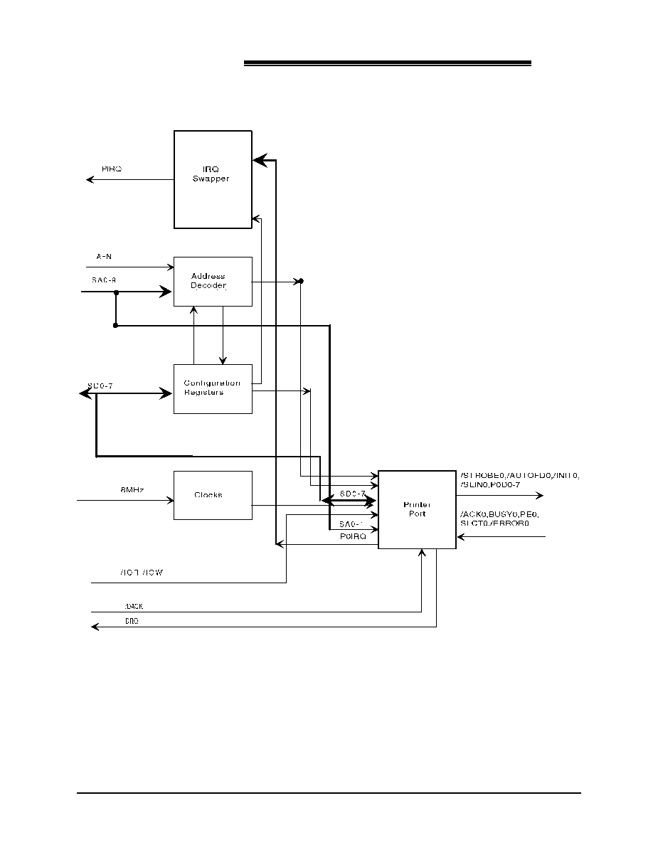
2087
ACC Micro
TM
113
Section 5.3
Block Diagram

2087
ACC Micro
TM
114
Section 5.4
Programmable Configuration Registers
Configuration registers in the 2087 are programmed with an indirect addressing scheme using I/O addresses F2
and F3. I/O address F2 contains the write-only configuration index register. F2 selects the corresponding
configuration register accessed at I/O address F3.
Configuration Register Index, BE (R/W)
Bit
Function
7-4
b7 b6 b5 b4 Read Threshold Write Threshold
0 0 0 0 15 1
0 0 0 1 14 2
0 0 1 0 13 3
0 0 1 1 12 4
0 1 0 0 11 5
0 1 0 1 10 6
0 1 1 0 9 7
0 1 1 1 8 8
1 0 0 0 7 9
1 0 0 1 6 10
1 0 1 0 5 11
1 0 1 1 4 12
1 1 0 0 3 13
1 1 0 1 2 14
1 1 1 0 1 15
3-2
Reserved
1-0
Parallel port mode selection
b1 b0
0 0 ECP/EPP
0 1 ECP
1 0 EPP
1 1 BPP/SPP
Configuration Register Index, BF (R/W)
Bit
Function
7-0
The 8 most significant address bits of the primary parallel port (A9-2).

2087
ACC Micro
TM
115
Section 5.5
Parallel Port Interface
The parallel port interface in the 2087 provides compatibility for a Centronics type printer. Its configuration
register allows the parallel port to be configured in PS/2 type bi-directional parallel port, Enhanced Parallel Port
(EPP) and Extended Capabilities Port (ECP) modes. Table 1 lists the registers associated with the parallel port
interface. The address map of the parallel port is shown below:
Data Port
=
Base Address + 00H
Status Port
=
Base Address + 01H
Control Port
=
Base Address + 02H
The microprocessor reads information on the parallel bus through Read Data register. The read and write
functions of a register are controlled by the state of the read pin (/IOR) and write pin (/IOW).
The microprocessor reads the status of the printer in the five most significant bits of the Read Status register.
Table 2 contains the bit definitions for this register.
Table 1
Parallel Port Interface Register Summary
Register
Bit 7
Bit 6
Bit 5
Bit 4
Bit 3
Bit 2
Bit 1
Bit 0
Read
Data
PD7
PD6
PD5
PD4
PD3
PD2
PD1
PD0
Read
Status
/BUSY
/ACK
PE
SLCT
/ERROR
0
0
TMOUT
Read
Control
0
0
PCD
= 1 Read
= 0 Write
IRQENB
SLIN
/INIT
AUTOF
D
STROBE
Write
Data
PD7
PD6
PD5
PD4
PD3
PD2
PD1
PD0
Write
Control
0
0
0
IRQENB
SLIN
/INIT
AUTOF
D
STROBE
Table 2
Read Status Register
Bit
Function
0
1
1
1
2
1
3
Error
4
Printer select
5
Paper Empty
6
Acknowledge
7
Printer busy

2087
ACC Micro
TM
116
The Read Control Register is for reading the state of the control lines. The Write Control Register sets the state
of the control lines. Table 3 contains the bit definitions for the Write Control Register.
Table 3
Write Control Register
Bit
Function
0
Strobe to inform the printer of the presence of a valid byte on the parallel port
1
Autofeed the paper
2
Initialize the printer
3
Select IN
4
Interrupt enable
5
Direction
6
Must be set to 1
7
Must be set to 1
The Microprocessor can write a byte to the parallel bus through the Write Data Register. When parallel ports
are set into extended mode (Bit 5, 2 of Register BE = 1), Control Bit 5 will control the direction of the parallel
ports.
When set to 1, the parallel ports can receive data from external devices. When set to 0, the parallel ports are
configured as the standard Centronics compatible parallel ports. Default is zero.
Decoder
The parallel port address decoder selects registers according to the states of the signals listed in Table 4.
Table 4
Address Decoder Register Selection
Control Signals
/IOR
/IOW
/CSPA
*A1
A0
Register Selected
0
1
0
0
0
Read Data register
0
1
0
0
1
Read Status register
0
1
0
1
0
Read Control register
0
1
0
1
1
Invalid
1
0
0
0
0
Write Data register
1
0
0
0
1
Invalid
1
0
0
1
0
Write Control register
1
0
0
1
1
Invalid
* /CSPA is an internal signal to parallel port logic.
Enhanced Parallel Port (EPP)
Beside the extended parallel port mode, the 2087 also supports the enhanced parallel port mode for greater
throughput. The address and data strobes can generate automatically to improve the transfer rate. The Status
Register and Control Register are available in Standard and Enhanced Parallel Port mode. In addition to this,
the address map for the EPP mode includes one address port and four data ports.

2087
ACC Micro
TM
117
EPP Register Configuration:
Register
Bit 7
Bit 6
Bit 5
Bit 4
Bit 3
Bit 2
Bit 1
Bit 0
EPP Address Port
AD7
PD6
PD5
PD4
PD3
PD2
PD1
PD0
EPP Data Port 0
PD7
PD6
PD5
PD4
PD3
PD2
PD1
PD0
EPP Data Port 1
PD7
PD6
PD5
PD4
PD3
PD2
PD1
PD0
EPP Data Port 2
PD7
PD6
PD5
PD4
PD3
PD2
PD1
PD0
EPP Data Port 3
PD7
PD6
PD5
PD4
PD3
PD2
PD1
PD0
The address map of the EPP is shown below: (Base Address = HEX 278 or 378)
EPP Address Port
=
Base Address + 03H
EPP Data Port 0
=
Base Address + 04H
EPP Data Port 1
=
Base Address + 05H
EPP Data Port 2
=
Base Address + 06H
EPP Data Port 3
=
Base Address + 07H
To access the EPP register, set the Write Control Register bit 3, 1,0 to zero. Multiple EPP access cycles can be
generated by software. When the parallel port is set to the compatible mode (Register BEh, bit 5 = 0), EPP
cycle can be generated to the external device by issuing the read and write cycle to the EPP register. When it is
set to the extended mode (Register BEh, bit 5 = 1), the EPP register returns the latch value for the read cycle in
the forward direction which set by the Write Control Register (bit 5 = 1). There will be no EPP read cycle in
this case. In the backward direction (Write Control Register bit 5 = 0), EPP write cycle is not available. Only
the EPP register data will be updated.
Procedure to Select Peripheral Device or Registers for EPP Specification 1.9 (Read Cycle):
1)
The host write a byte to the EPP address register. When /IOR goes low, EPP also pulls IOCHRDY low
and wait for /WAIT to go low.
2)
Once /WAIT goes low, EPP pulls /ADDRSTRB or /DATASTRB low to indicate PD0-PD7 is tri-
stated.
3)
The peripheral drives PD0-PD7 valid.
4)
Peripheral pulls /WAIT low, indicating PD0-PD7 is valid. The phase of the cycle can be terminated.
5)
The chip latches the data from the PData bus for SData bus then deasserts /ADDRSTRB or
/DATASTRB
to begin teminate the cycle. The chip then drives valid data onto the SData bus and
pulls IOCHRDY high allowing the host to complete the read cycle.
6)
PD0-PD7 tri-states by the peripheral and the chip may modify /WRITE and ready for next cycle.

2087
ACC Micro
TM
118
Procedure to Select Peripheral Device or Registers for EPP Specification 1.9 (Write Cycle):
1)
The host write a byte to the EPP address register. When /IOW goes low, EPP also pulls IOCHRDY
low and wait for /WAIT to go low. EPP also places data on the SData bus.
2)
Once /WAIT goes low, EPP pulls /ADDRSTRB or /DATASTRB low to indicate PData bus contains
valid data.
3)
Peripheral pulls /WAIT low, indicating PD0-PD7 is valid. The phase of the cycle can be terminated.
4)
The chip latches the data from the PData bus for SData bus then deasserts /ADDRSTRB or
/DATASTRB to begin teminate the cycle. The chip then drives valid data onto the SData bus and pulls
IOCHRDY high allowing the host to complete the write cycle.
5)
/WAIT asserts by the peripheral to acknowledge the termination of the cycle and the chip may modify
/WRITE and ready for next cycle.
When the EPP mode is selected, the standard mode and extended modes are also available.
Extended Capability Port (ECP)
The ECP mode is also supported by the ACC 2087 with a 16bytes FIFO. The address map and ECP register
configuration of the ECP are shown below:
Address Map: (Base Address = 278h or 378h)
Data Port
:
Base Address + 000h
ECPAFIFO
:
Base Address + 000h
DSR
:
Base Address + 001h
DCR
:
Base Address + 002h
ECPCFIFO
:
Base Address + 400h
ECPDFIFO
:
Base Address + 400h
TFIFO
:
Base Address + 400h
CNFGA
:
Base Address + 400h
CNFGB
:
Base Address + 401h
ECR
:
Base Address + 402h
ECP Register Configuration:
ECPAFIFO - ECP FIFO Address / RLE (Mode 011)
Bit
Description
7
Write only. This bit is used to indicate data type.
When set to 1, bits [6:0] are a ECP address.
When set to 0, bit field [6:0] is a run length. It is used to indicate how many times the next data will
be appeared. ( for example: [6:0] = 0 is 1 time, [6:0] = 1 is 2 times, [6:0] = 2 is 3 times, etc.
6-0
Write only. This is a ECP address or run length encode (RLE) as described above.

2087
ACC Micro
TM
119
DSR - Device Status Register (Mode All)
Bit
Description
7
Read only. nBUSY. This indicates a inverted version of parallel port BUSY signal.
6
Read only. nACK. This indicates a version of parallel port nACK signal.
5
Read only. PERROR. This indicates a version of parallel port PERROR signal.
4
Read only. SELECT. This indicates a version of parallel port SELECT signal.
3
Read only. nFAULT. This indicates a version of parallel port nFAULT signal.
2-0
Reserved.
DCR - Device Control Register (Mode All)
Bit
Description
7-6
Reserved.
5
Read/Write. Direction.
When set to 0, DMA and data are written to the peripheral. The drivers are enabled.
When set to 1, if it is in standard parallel port mode (mode 000 or 010), this bit has no effect. If it is
in ECP mode, the drivers is tri-stated and it sets the direction so that data will be read from the
peripheral.
4
Read/Write. When set to 0, it disables the nACK interrupt. When set to 1, it enables an interrupt on
the rising edge of nACK.
3
Read/Write. When set to 0, this bit has no effect. When set to 1, it forces the SELECTIN signal low
regardless of the hardware state machine even in ECP mode. Software should make sure that bit 3 is
set to 0 prior to entering ECP mode.
2
Read/Write. When set to 0, this bit has no effect. When set to 1, it forces the nINIT signal active
regardless of the hardware state machine.
1
Read/Write. When set to 0, this bit has no effect. When set to 1, it forces the AUTOFD signal low
regardless of the hardware state machine even in ECP mode. Software should make sure that bit 1 is
set to 0 prior to entering ECP mode.
0
Read/Write. When set to 0, this bit has no effect. When set to 1, it forces the STROBE signal low
regardless of the hardware state machine even in ECP mode. Software should make sure that bit 0 is
set to 0 prior to entering ECP mode.
CFIFO - Parallel Port Data FIFO (Mode 011)
This mode is only defined for forward direction. The hardware standard parallel port protocol is used to
transmit the bytes written or DMAed, from the system to this FIFO, to the peripheral. Transfers to the FIFO are
bytes aligned.
ECPDFIFO - ECP Data FIFO (Mode 011)
When DCR (Device Control Register) bit 5 is set to 0, the hardware ECP parallel port protocol is used to
transmit the bytes written or DMAed , from the system to this FIFO, to the peripheral. Transfer to the FIFO are
bytes aligned. When DCR bit 5 is set to 1, data from the peripheral are read under automatic hardware
handshake from ECP into the FIFO.

2087
ACC Micro
TM
120
TFIFO - Test Mode (Mode 110)
Data may be read, written or DMAed to or from the system to this FIFO in any direction.
Data in the TFIFO will not be transmitted to the parallel port lines using a hardware protocol handshake,
However, data in the TFIFO may be displayed on the parallel port data lines.
The TFIFO will not stall when overwritten or underrun. Data will simply be re-written or over-run. The full
and empty bits must always keep track of the correct FIFO state. The TFIFO will transfer data at the maximum
ISA rate so that software may generated performance metrics.
Data PWords are always read from the head of TFIFO regardless of the value of the direction bit. The FIFO
size and interrupt threshold can be determined by writing PWords and checking the full and service interrupt
bits.
CNFGA - Configuration Resister A (Mode 111)
This is a read only register.
CNFGB - Configuration Register B (Mode 111)
Bit
Description
7
Reserved. Always 0.
6
Read only. Its value on the ISA interrupt line determines the possible conflicts. Default 1.
5-0
Reserved. Always 0.
ECR - Extended Control Register
Bit
Description
7-5
Read/Write.
When set to 000, the standard parallel port mode is selected. In this mode the FIFO is reset and
common collector drivers are used on the control lines. Setting the direction bit will not tri-state the
output drivers in this mode.
When set to 001, the PS/2 parallel port mode is selected. This is the same as the standard parallel
mode except that direction may be used to tri-state the data lines and reading the data register returns
the value on the data lines and not the value in the data register.
When set to 010, the parallel port FIFO mode is selected. This is the same as the standard parallel
port mode except that PWords are written or DMAed to the FIFO. FIFO data is automatically
transmitted using the standard parallel port protocol. Note that this mode is only useful when
direction is 0. All drivers have active pull-ups.
When set to 011, the ECP parallel port mode is selected. In the forward direction PWords placed
into the ECPDFIFO and bytes written to the ECPAFIFO are placed in a single FIFO and transmitted
automatically to the peripheral using ECP protocol. In the reverse direction bytes are moved from
the ECP parallel port and packed into PWords in the ECPDFIFO.
When set to 110, the test mode is selected.
When set to 111, configuration register A,B are accessible at 0x400 and 0x401.
When set to 100, the EPP parallel port mode is selected.

2087
ACC Micro
TM
116
Section 6
DC Specifications
2087 Rating Specifications
Absolute Maximum Ratings*
Parameter
Symbol
Condition
Min
Max
Unit
Power supply voltage
VDD
Ta=25 C
VSS-0.3
7.0
V
Input voltage
VI
VSS-0.3
VDD+0.5
V
Output voltage
VO
VSS-0.3
VDD+0.5
V
Operating temperature
Top
0
70.0
C
Storage temperature
Tstg
-65.0
150.0
C
*
Exposing the device to stress above these limits can cause permanent damage. The device is not meant
to
be operated under conditions outside the limits described in the operational sections of this
specification. Exposure to absolute maximum rating conditions for extended periods can affect device
reliability.
Capacitance Limits
TA = +25 C, VDD = 3.3V or 5.0V
Parameter
Symbol
Min
Typ
Max
Unit
Test Condition
Input capacitance
CI
4.0
pF
fc = 1.0 MHz
Output capacitance
CO
6.0
I/O capacitance
CIO
10.0
pF
2087
ACC Micro
TM
117
DC Specifications
TA = 0 C to 70 C, VDD = 5.0V +/- 5%
X14M#, X24M
Parameter
Symbol
Min
Max
Unit
Test Condition
Input low voltage
VIL
VSS
1
V
VDD = 5.0V +/- 5%
Input high voltage
VIH
3.5
VDD
V
VDD = 5.0V +/- 5%
Input low current
IIL
-1
1
uA
VIN = VSS
Input high current
IIH
-1
1
uA
VIN = VDD
SUSPACK
Parameter
Symbol
Min
Max
Unit
Test Condition
Schmitt trigger Input low
voltage
VIL
0.6
V
VDD = 5.0V +/- 5%
Schmitt trigger Input High
voltage
VIH
3
V
VDD = 5.0V +/- 5%
Input low current
IIL
-1
1
uA
VIN = VSS
Input high current
IIH
-1
1
uA
VIN = VDD
ZWS#, MASTER#
Parameter
Symbol
Min
Max
Unit
Test Condition
Input low voltage
VIL
VSS
0.8
V
VDD = 5.0V +/- 5%
Input high voltage
VIH
2
VDD
V
VDD = 5.0V +/- 5%
Input low current
IIL
-105
-25
uA
VIN = VSS
Input high current
IIH
-1
1
uA
VIN = VDD
READY0#, LBA#, RTCINT#, IRQ5, IRQ7, IRQ9-11, IRQ14, DRQ0, DRQ5, EXTSMI0, EXTSMI1, SRBTN#,
INDEX#, TRK0#, WP#, RDDATA#,DSCKCHG#, RX1-2, CTS#1-2, DSR#1-2, DCD#1-2, RI#1-2, LPTERR#,
LPTBZY, SLCT, PE, LPTACK#
Parameter
Symbol
Min
Max
Unit
Test Condition
Input low voltage
VIL
VSS
0.8
V
VDD = 5.0V +/- 5%
Input high voltage
VIH
2
VDD
V
VDD = 5.0V +/- 5%
Input low current
IIL
-105
-25
uA
VIN = VSS
Input high current
IIH
-1
1
uA
VIN = VDD

2087
ACC Micro
TM
118
CPUBZY#, MA486, SPRK, PWRCNTL3-7, STPGNT#, SUSPMOD#, RTCAS, XDIR#
Parameter
Symbol
Min
Max
Unit
Test Condition
Output low voltage
VOL
VSS+0.4
V
IOL = 4.0 mA
Output high voltage
VOH
VDD-0.4
V
IOH = -4.0 mA
SDDIR#
Parameter
Symbol
Min
Max
Unit
Test Condition
Output low voltage
VOL
VSS+0.4
V
IOL = 2.0 mA
Output high voltage
VOH
VDD-0.4
V
IOH = -2.0 mA
BALE, AEN, TC, STPCLK#, SMI#
Parameter
Symbol
Min
Max
Unit
Test Condition
Output low voltage
VOL
VSS+0.4
V
IOL = 12.0 mA
Output high voltage
VOH
VDD-0.4
V
IOH = -12.0 mA
DACK5#
Parameter
Symbol
Min
Max
Unit
Test Condition
Output low voltage
VOL
VSS+0.4
V
IOL = 4.0 mA
Output high voltage
VOH
VDD-0.4
V
IOH = -4.0 mA
Tristate leakage current
IOZ
-1
1
uA
VOUT = VDD or VSS
SMEMR#, SMEMW#
Parameter
Symbol
Min
Max
Unit
Test Condition
Output low voltage
VOL
VSS+0.4
V
IOL = 12.0 mA
Output high voltage
VOH
VDD-0.4
V
IOH = -12.0 mA
Tristate leakage current
IOZ
-1
1
uA
VOUT = VDD or VSS
2087
ACC Micro
TM
119
DTR1#, RTS1#
Parameter
Symbol
Min
Max
Unit
Test Condition
Output low voltage
VOL
VSS+0.4
V
IOL = 2.0 mA
Output high voltage
VOH
VDD-0.4
V
IOH = -2.0 mA
Tristate leakage current
IOZ
-1
1
uA
VOUT = VDD or VSS
MO1#, DACK2#, FDCWE#, FDCIR#, HEAD#, WRDATA#, STEP#, RWC#
Parameter
Symbol
Min
Max
Unit
Test Condition
Output low voltage
VOL
VSS+0.4
V
IOL = 24.0 mA
Output high voltage
VOH
VDD-0.4
V
IOH = -24.0 mA
Tristate leakage current
IOZ
-1
1
uA
VOUT = VDD or VSS
DACK0#
Parameter
Symbol
Min
Max
Unit
Test Condition
Input low voltage
VIL
VSS
0.8
V
VDD = 5.0V +/- 5%
Input high voltage
VIH
2
VDD
V
VDD = 5.0V +/- 5%
Input low current
IIL
-105
-25
uA
VIN = VSS
Input high current
IIH
-1
1
uA
VIN = VDD
Output low voltage
VOL
VSS+0.4
V
IOL = 4.0 mA
Output high voltage
VOH
VDD-0.4
V
IOH = -1.0 mA
Tristate Leakage current
IOZ
-105
-25
uA
VOUT = VDD or VSS
MEMCS16#, IOCS16#, IOCHRDY
Parameter
Symbol
Min
Max
Unit
Test Condition
Input low voltage
VIL
VSS
0.8
V
VDD = 5.0V +/- 5%
Input high voltage
VIH
2
VDD
V
VDD = 5.0V +/- 5%
Input low current
IIL
-105
-25
uA
VIN = VSS
Input high current
IIH
-1
1
uA
VIN = VDD
Output low voltage
VOL
VSS+0.4
V
IOL = 12.0 mA
Output high voltage
VOH
VDD-0.4
V
IOH = -2.0 mA
Tristate Leakage current
IOZ
-105
-25
uA
VOUT = VDD or VSS

2087
ACC Micro
TM
120
SD0-SD15, SA0, SA1, SMIADS#, SMIACT#, MEMR#, MEMW#, IOR#, IOW#, REF#, SBHE#
Parameter
Symbol
Min
Max
Unit
Test Condition
Input low voltage
VIL
VSS
0.8
V
VDD = 5.0V +/- 5%
Input high voltage
VIH
2
VDD
V
VDD = 5.0V +/- 5%
Input low current
IIL
-105
-25
uA
VIN = VSS
Input high current
IIH
-1
1
uA
VIN = VDD
Output low voltage
VOL
VSS+0.4
V
IOL = 12.0 mA
Output high voltage
VOH
VDD-0.4
V
IOH = -4.0 mA
Tristate Leakage current
IOZ
-105
-25
uA
VOUT = VDD or VSS
RESETDRV#
Parameter
Symbol
Min
Max
Unit
Test Condition
Output low voltage
VOL
VSS+0.4
V
IOL = 8.0 mA
Output high voltage
VOH
VDD-0.4
V
IOH = -2.0 mA
Tristate Leakage current
IOZ
-1
1
uA
VOUT = VDD or VSS
ENSDL#, ENSDH#, TX1, TX2, DTR2#, RTS2#
Parameter
Symbol
Min
Max
Unit
Test Condition
Input low voltage
VIL
VSS
0.8
V
VDD = 5.0V +/- 5%
Input high voltage
VIH
2
VDD
V
VDD = 5.0V +/- 5%
Input low current
IIL
-105
-25
uA
VIN = VSS
Input high current
IIH
-1
1
uA
VIN = VDD
Output low voltage
VOL
VSS+0.4
V
IOL = 2.0 mA
Output high voltage
VOH
VDD-0.4
V
IOH = -1.0 mA
Tristate Leakage current
IOZ
-105
-25
uA
VOUT = VDD or VSS
MO0#, DRQ2, DS0, IRQ6, DS1, ENFDC
Parameter
Symbol
Min
Max
Unit
Test Condition
Input low voltage
VIL
VSS
0.8
V
VDD = 5.0V +/- 5%
Input high voltage
VIH
2
VDD
V
VDD = 5.0V +/- 5%
Input low current
IIL
-105
-25
uA
VIN = VSS
Input high current
IIH
-1
1
uA
VIN = VDD
Output low voltage
VOL
VSS+0.4
V
IOL = 24.0 mA
Output high voltage
VOH
VDD-0.4
V
IOH = -12.0 mA
Tristate Leakage current
IOZ
-105
-25
uA
VOUT = VDD or VSS

2087
ACC Micro
TM
121
ID7#
Parameter
Symbol
Min
Max
Unit
Test Condition
Input low voltage
VIL
VSS
0.8
V
VDD = 5.0V +/- 5%
Input high voltage
VIH
2
VDD
V
VDD = 5.0V +/- 5%
Input low current
IIL
-105
-25
uA
VIN = VSS
Input high current
IIH
-1
1
uA
VIN = VDD
Output low voltage
VOL
VSS+0.4
V
IOL = 8.0 mA
Output high voltage
VOH
VDD-0.4
V
IOH = -4.0 mA
Tristate Leakage current
IOZ
-105
-25
uA
VOUT = VDD or VSS
STB#, ATFD#, INIT#, SLIN#, PD0-PD7
Parameter
Symbol
Min
Max
Unit
Test Condition
Input low voltage
VIL
VSS
0.8
V
VDD = 5.0V +/- 5%
Input high voltage
VIH
2
VDD
V
VDD = 5.0V +/- 5%
Input low current
IIL
-105
-25
uA
VIN = VSS
Input high current
IIH
-1
1
uA
VIN = VDD
Output low voltage
VOL
VSS+0.4
V
IOL = 12.0 mA
Output high voltage
VOH
VDD-0.4
V
IOH = -6.0 mA
Tristate Leakage current
IOZ
-105
-25
uA
VOUT = VDD or VSS
2087
ACC Micro
TM
122
TA = 0 C to 70 C, VDD = 3.3 V +/- 5%
PWRGD, TURBO
Parameter
Symbol
Min
Max
Unit
Test Condition
Schmitt trigger Input low
voltage
VIL
0.6
V
VDD = 3.3V +/- 5%
Schmitt trigger Input High
voltage
VIH
3.0
V
VDD = 3.3V +/- 5%
Input low current
IIL
-1
1
uA
VIN = VSS
Input high current
IIH
-1
1
uA
VIN = VDD
CLKSRC, CLKI, HLDA, NPEREQ
Parameter
Symbol
Min
Max
Unit
Test Condition
Input low voltage
VIL
VSS
0.8
V
VDD = 3.3V +/- 5%
Input high voltage
VIH
2
VDD
V
VDD = 3.3V +/- 5%
Input low current
IIL
-105
-25
uA
VIN = VSS
Input high current
IIH
-1
1
uA
VIN = VDD
D/-C, NPERR#, ALARM, EXTSYS#, ACPWR, LBAT1
Parameter
Symbol
Min
Max
Unit
Test Condition
Input low voltage
VIL
VSS
0.8
V
VDD = 3.3V +/- 5%
Input high voltage
VIH
2
VDD
V
VDD = 3.3V +/- 5%
Input low current
IIL
-105
-25
uA
VIN = VSS
Input high current
IIH
-1
1
uA
VIN = VDD
CPURST, CLKx1, CLKx2, NA#
Parameter
Symbol
Min
Max
Unit
Test Condition
Output low voltage
VOL
VSS+0.4
V
IOL = 4.0 mA
Output high voltage
VOH
VDD-0.4
V
IOH = -2.0 mA
PWRCNTL0-1
Parameter
Symbol
Min
Max
Unit
Test Condition
Output low voltage
VOL
VSS+0.4
V
IOL = 8.0 mA
Output high voltage
VOH
VDD-0.4
V
IOH = -4.0 mA

2087
ACC Micro
TM
123
PWRCNTL2, PHOLD, INTR, NMI, KTGOE, GA20, MDIR#
Parameter
Symbol
Min
Max
Unit
Test Condition
Output low voltage
VOL
VSS+0.4
V
IOL = 2.0 mA
Output high voltage
VOH
VDD-0.4
V
IOH = -1.0 mA
SYSCLK#, WEN#, RAS0#, RAS2#, CAS#0-3
Parameter
Symbol
Min
Max
Unit
Test Condition
Output low voltage
VOL
VSS+0.4
V
IOL = 12.0 mA
Output high voltage
VOH
VDD-0.4
V
IOH = -6.0 mA
CPUPEREQ, BS16#
Parameter
Symbol
Min
Max
Unit
Test Condition
Output low voltage
VOL
VSS+0.4
V
IOL = 4.0 mA
Output high voltage
VOH
VDD-0.4
V
IOH = -2.0 mA
Tristate leakage current
IOZ
-1
1
uA
VOUT = VDD or VSS
RAS1#, RAS3#
Parameter
Symbol
Min
Max
Unit
Test Condition
Output low voltage
VOL
VSS+0.4
V
IOL = 12.0 mA
Output high voltage
VOH
VDD-0.4
V
IOH = -6.0 mA
Tristate leakage current
IOZ
-1
1
uA
VOUT = VDD or VSS
ADS#, M/-IO, W/-R, RDY#, NPBZY#, FLUSH#
Parameter
Symbol
Min
Max
Unit
Test Condition
Input low voltage
VIL
VSS
0.8
V
VDD = 3.3V +/- 5%
Input high voltage
VIH
2
VDD
V
VDD = 3.3V +/- 5%
Input low current
IIL
-105
-25
uA
VIN = VSS
Input high current
IIH
-1
1
uA
VIN = VDD
Output low voltage
VOL
VSS+0.4
V
IOL = 4.0 mA
Output high voltage
VOH
VDD-0.4
V
IOH = -2.0 mA
Tristate Leakage current
IOZ
-105
-25
uA
VOUT = VDD or VSS
BE0#-BE3#, A2-A25, A31, LA20, D0-D15, KTGWE#
Parameter
Symbol
Min
Max
Unit
Test Condition
Input low voltage
VIL
VSS
0.8
V
VDD = 3.3V +/- 5%
Input high voltage
VIH
2
VDD
V
VDD = 3.3V +/- 5%
Input low current
IIL
-105
-25
uA
VIN = VSS
Input high current
IIH
-1
1
uA
VIN = VDD
Output low voltage
VOL
VSS+0.4
V
IOL = 4.0 mA
Output high voltage
VOH
VDD-0.4
V
IOH = -2.0 mA
Tristate Leakage current
IOZ
-105
-25
uA
VOUT = VDD or VSS
2087
ACC Micro
TM
124
KRMOE#, KRMWE#
Parameter
Symbol
Min
Max
Unit
Test Condition
Input low voltage
VIL
VSS
0.8
V
VDD = 3.3V +/- 5%
Input high voltage
VIH
2
VDD
V
VDD = 3.3V +/- 5%
Input low current
IIL
-105
-25
uA
VIN = VSS
Input high current
IIH
-1
1
uA
VIN = VDD
Output low voltage
VOL
VSS+0.4
V
IOL = 8.0 mA
Output high voltage
VOH
VDD-0.4
V
IOH = -4.0 mA
Tristate Leakage current
IOZ
-105
-25
uA
VOUT = VDD or VSS
MA0-MA10
Parameter
Symbol
Min
Max
Unit
Test Condition
Input low voltage
VIL
VSS
0.8
V
VDD = 3.3V +/- 5%
Input high voltage
VIH
2
VDD
V
VDD = 3.3V +/- 5%
Input low current
IIL
-105
-25
uA
VIN = VSS
Input high current
IIH
-1
1
uA
VIN = VDD
Output low voltage
VOL
VSS+0.4
V
IOL = 12.0 mA
Output high voltage
VOH
VDD-0.4
V
IOH = -6.0 mA
Tristate Leakage current
IOZ
-105
-25
uA
VOUT = VDD or VSS
TGLA2-TGLA3
Parameter
Symbol
Min
Max
Unit
Test Condition
Output low voltage
VOL
VSS+0.4
V
IOL = 8.0 mA
Output high voltage
VOH
VDD-0.4
V
IOH = -4.0 mA
Tristate Leakage current
IOZ
-1
1
uA
VOUT = VDD or VSS
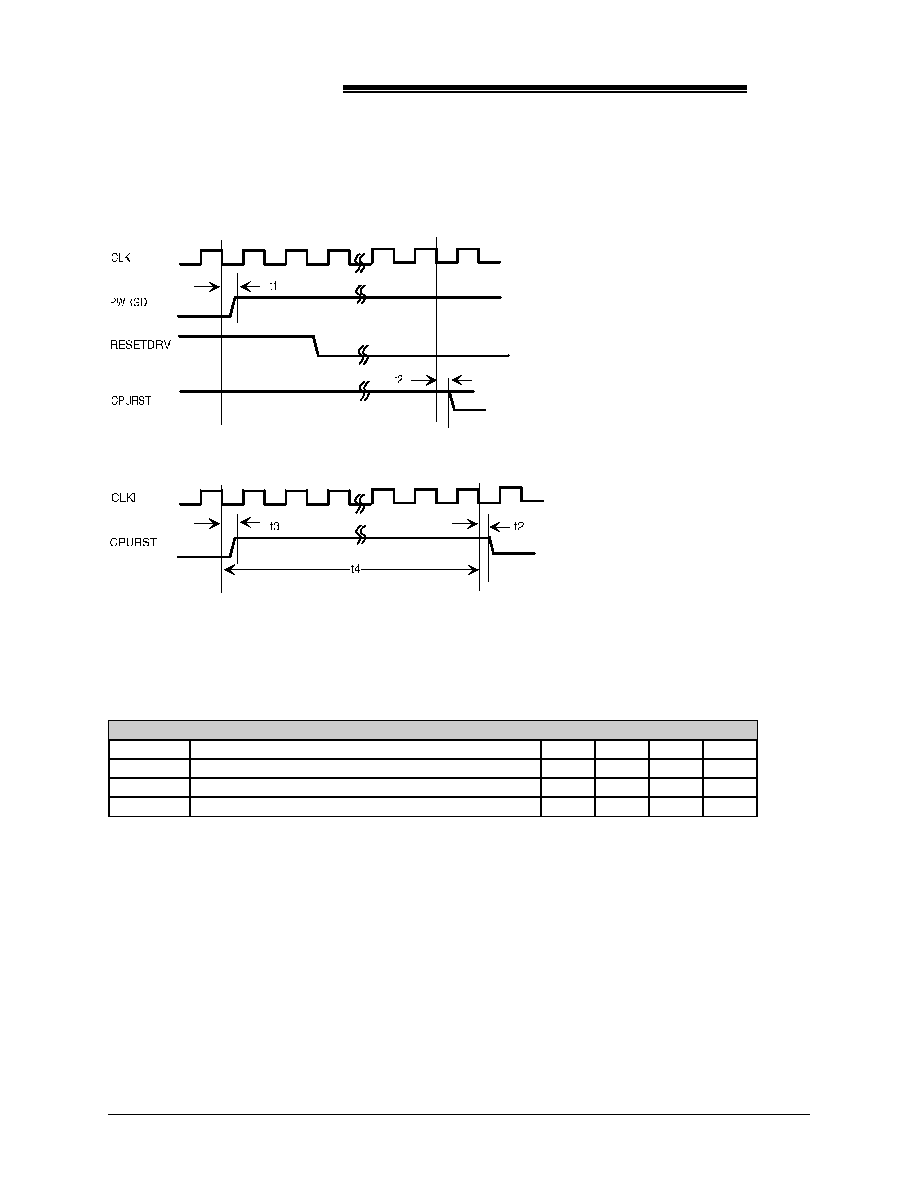
2087
ACC Micro
TM
125
Section 7
2087 AC Specifications
Cold Reset
Warm Reset
AC Specifications
The default load of output signal is 100 pf. The output load which is not 100 pf will specify in load item.
Symbol
Parameter
Min
Typ
Max
Units
t1
RESETDRV deactive from falling edge of CLKI
3
10
ns
t2
CPURST deactive from falling edge of CLKI
3
10
ns
t3
CPURST active from falling edge of CLKI
9
ns
t4
CPURST active period for warm reset
16us
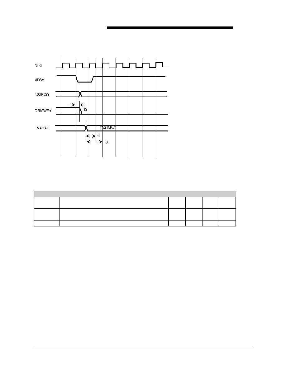
2087
ACC Micro
TM
126
Internal Comparator Timing
AC Specifications
The default load of output signal is 100 pf. The output load which is not 100 pf will specify in load item.
Symbol
Parameter
Min
Typ
Max
Units
t1
In cache write, the TAG setup time for CLKI falling
edge for internal comparator
3
10
ns
t2
In cache read, the TAG setup time for CLKI rising
edge for internal comparator
3
10
ns
t3
DRMWE# activate from the rising edge of CLKI
3
9
ns
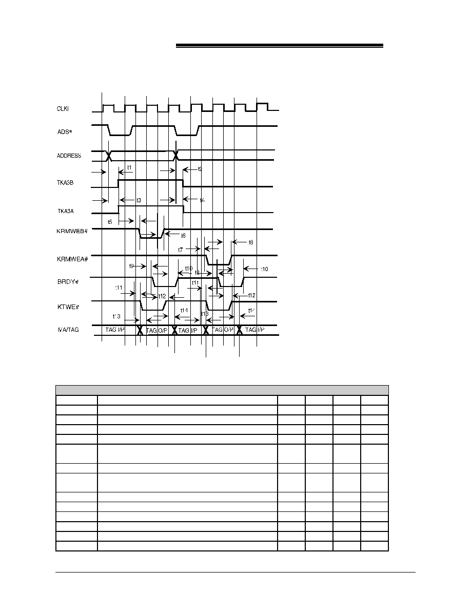
2087
ACC Micro
TM
127
Cache Write Hit Timing
AC Specifications
The default load of output signal is 100 pf. The output load which is not 100 pf will specify in load item.
Symbol
Parameter
Min
Typ
Max
Units
t1
TKA3B activate delay from Address
2
7
ns
t2
TKA3B deactivate delay from Address
3
9
ns
t3
TKA3A activate delay from Address
2
7
ns
t4
TKA3A deactivate delay from Address
3
9
ns
t5
KRMWEB# activate delay from CLKI falling edge
4
12
ns
t6
KRMWEB# deactivate delay from CLKI falling
edge
4
11
ns
t7
KRMWEA# activate delay from CLKI falling edge
3
12
ns
t8
KRMWEA# deactivate delay from CLKI falling
edge
4
11
ns
t9
CPURDY# activate delay from CLKI rising edge
5
16
ns
t10
CPURDY# deactivate delay from CLKI rising edge
5
16
ns
t11
KTGWE# activate delay from CLKI falling edge
5
14
ns
t12
KTGWE# deactivate delay from CLKI falling edge
4
13
ns
t13
TAG output delay from CLKI falling edge
6
17
ns
t14
TAG input delay from CLKI rising edge
5
16
ns
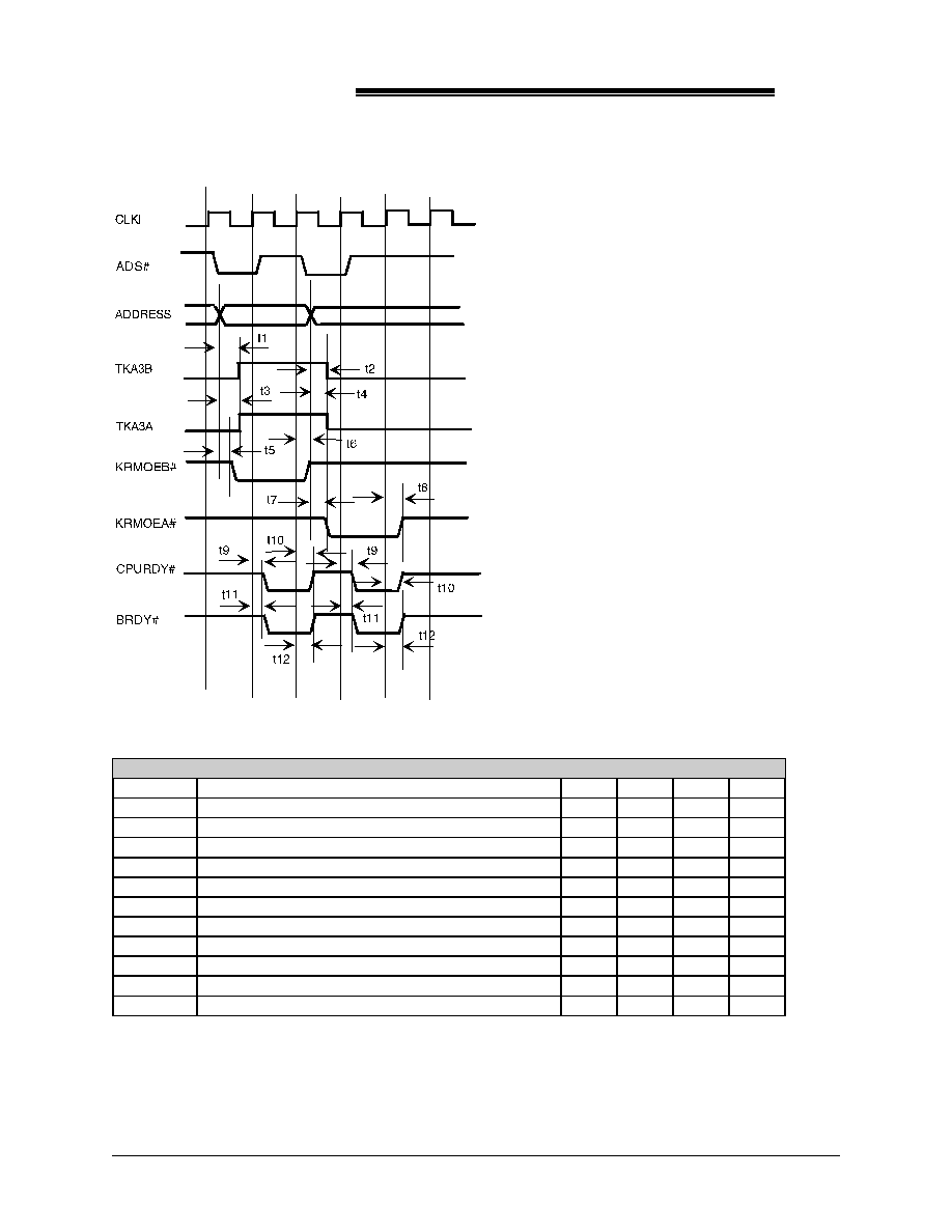
2087
ACC Micro
TM
128
Cache Read Hit Timing
AC Specifications
The default load of output signal is 100 pf. The output load which is not 100 pf will specify in load item.
Symbol
Parameter
Min
Typ
Max
Units
t1
TKA3B activates from Address
2
7
ns
t2
TKA3B deactivates from Address
3
9
ns
t3
TKA3A activates from Address
2
7
ns
t4
TKA3A deactivates from Address
3
9
ns
t5
KRMOEB# activates from ADS# active
7
20
ns
t6
KRMOEB# deactivates from CLKI# rising edge
4
11
ns
t7
KRMOEA# activates from ADS# activate
7
21
ns
t8
KRMOEA# deactivate from CLKI rising edge
4
11
ns
t9
CPURDY# activates from CLKI rising edge
5
16
ns
t10
CPURDY# deactivates from CLKI rising edge
5
16
ns
t11
BRDY# activates from CLKI rising edge
5
16
ns
t12
CPURDY# deactivates from CLKI rising edge
5
15
ns
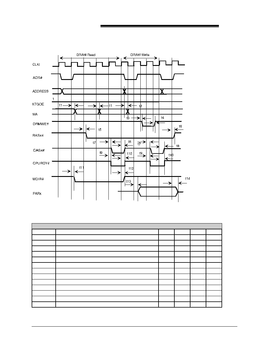
2087
ACC Micro
TM
129
DRAM Access with Cache Disable
AC Specifications
The default load of output signal is 100 pf. The output load which is not 100 pf will specify in load item.
Symbol
Parameter
Min
Typ
Max
Units
t1
MA delay from CLKI rising edge
6
18
ns
t2
MA delay from Address valid
6
19
ns
t3
DRMWE# active delay from CLKI falling edge
4
12
ns
t4
DRMWE# deactive delay from CLKI falling edge
4
11
ns
t5
RAS# active delay from CLKI rising edge
3
10
ns
t6
RAS# deactive delay from CLKI rising edge
3
10
ns
t7
CAS# activate delay from CLKI rising edge
3
10
ns
t8
CAS# deactivate delay from CLKI rising edge
3
10
ns
t9
CPURDY# activate delay from CLKI rising edge
6
18
ns
t10
CPURDY# deactivate delay from CLKI rising edge
6
18
ns
t11
MDIR# activate delay from CLKI rising edge
3
10
ns
t12
MDIR# deactivate delay from CLKI rising edge
3
9
ns
t13
PARx output from CLKI rising edge
7
20
ns
t14
PARx hold time from CLKI rising edge
7
22
ns
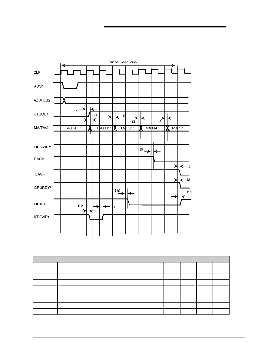
2087
ACC Micro
TM
130
DRAM Access with Cache Enable
1 of 2
AC Specifications
The default load of output signal is 100 pf. The output load which is not 100 pf will specify in load item.
Symbol
Parameter
Min
Typ
Max
Units
t1
KTGOE# deactive from CLKI rising edge
4
11
ns
t2
KTGOE# activate from CLKI rising edge
4
12
ns
t3
MA delay from CLKI rising edge
6
18
ns
t4
MA delay from Address valid
6
19
ns
t5
RAS# activate from CLKI rising edge
3
10
ns
t6
CAS# activate from CLKI rising edge
3
10
ns
t7
CAS# deactivate from CLKI rising edge
3
10
ns
t8
CPURDY# activate from CLKI rising edge
6
19
ns
t9
CPURDY# deactivate from CLKI rising edge
6
19
ns

2087
ACC Micro
TM
131
DRAM Access with Cache Enable
2 of 2
AC Specifications
The default load of output signal is 100 pf. The output load which is not 100 pf will specify in load item.
Symbol
Parameter
Min
Typ
Max
Units
t10
MDIR# activate from CLKI rising edge
3
10
ns
t11
MDIR# deactivate from CLKI rising edge
3
10
ns
t12
KTGWE# activate from CLKI rising edge
4
12
ns
t13
KTGWE# deactivate from CLKI rising edge
4
11
ns
t14
PARx output from CLKI rising edge
7
20
ns
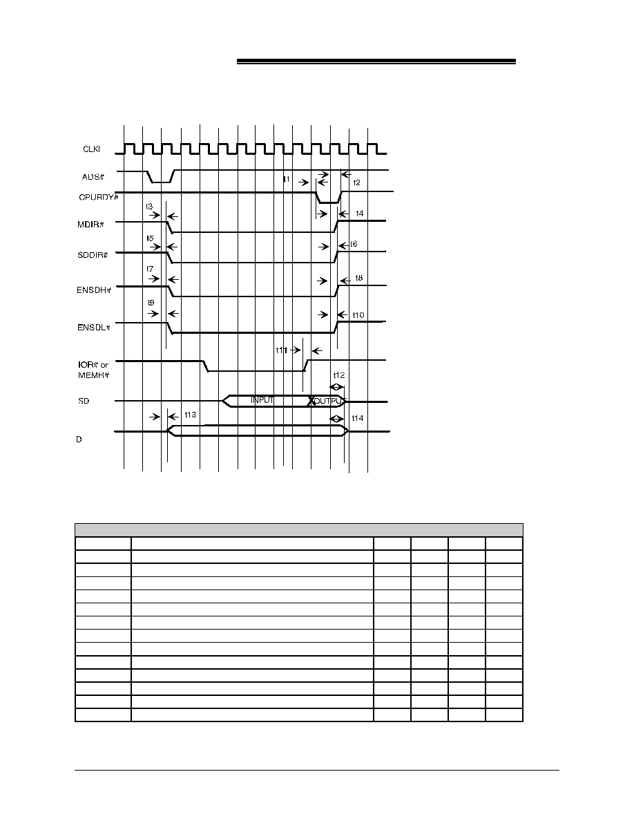
2087
ACC Micro
TM
132
AT Bus Read
AC Specifications
The default load of output signal is 100 pf. The output load which is not 100 pf will specify in load item.
Symbol
Parameter
Min
Typ
Max
Units
t1
CPURDY# activate from CLKI rising edge
5
16
ns
t2
CPURDY# deactivate from CLKI rising edge
6
19
ns
t3
MDIR# activate from CLKI rising edge
3
10
ns
t4
MDIR# deactivate from CLKI rising edge
3
9
ns
t5
SDDIR# activate from CLKI rising edge
8
24
ns
t6
SDDIR# deactivate from CLKI rising edge
6
17
ns
t7
ENSDH# activate from CLKI rising edge
7
22
ns
t8
ENSDH# deactivate from CLKI rising edge
7
21
ns
t9
ENSDL# deactivate from CLKI rising edge
8
25
ns
t10
ENSDL# deactivate from CLKI rising edge
7
20
ns
t11
SD input hold time from command deactivate
0
ns
t12
SD hold time from CLKI2I rising edge
6
18
ns
t13
D becomes input from CLK2I rising edge
7
22
ns
t14
D hold time from CLK2I rising edge
6
19
ns

2087
ACC Micro
TM
133
AT Bus Write
AC Specifications
The default load of output signal is 100 pf. The output load which is not 100 pf will specify in load item.
Symbol
Parameter
Min
Typ
Max
Units
t1
CPURDY# activate from CLKI
5
16
ns
t2
CPURDY# deactivate from CLKI
6
19
ns
t3
ENSDH# activate from CLKI
7
22
ns
t4
ENSDH# deactivate from CLKI
7
21
ns
t5
ENSDH# activate from CLKI
8
25
ns
t6
ENSDL# deactivate from CLKI
7
20
ns
t7
SD becomes output from CLKI
20
60
ns
t8
LSD hold time from CLKI
7
22
ns

2087
ACC Micro
TM
134
Cache Read Miss Dirty
1 of 2

2087
ACC Micro
TM
135
Cache Read Miss Dirty
2 of 2

2087
ACC Micro
TM
136
AC Specifications
The default load of output signal is 100 pf. The output load which is not 100 pf will specify in load item.
Symbol
Parameter
Min
Typ
Max
Units
t1
KTGOE deactivate from CLKI rising edge
4
11
ns
t2
KTGOE activate from CLKI rising edge
4
12
ns
t3
MA/TAG valid from CLKI rising edge
6
17
ns
t4
KTGWE# activate from CLKI rising edge
5
14
ns
t5
KTGWE# deactivate from CLKI rising edge
4
13
ns
t6
WEN# activate from CLKI falling edge
4
12
ns
t7
WEN# deactivate from CLKI falling edge
4
11
ns
t8
CAS# activate from CLKI rising edge
3
10
ns
t9
CAS# deactivate from CLKI rising edge
3
9
ns
t10
TKA3B# activate from CLKI rising edge
5
16
ns
t11
TAK3B deactivate from CLKI rising edge
4
12
ns
t12
TKA2A activate from CLKI rising edge
5
16
ns
t13
TKA2A deactivate from CLK2 rising edge
4
12
ns
t14
KRMOEB# activate from CLKI rising edge
4
13
ns
t15
KRMOEB# deactivate from CLK2 rising edge
4
12
ns
t16
KRMOEA# activate from CLKI rising edge
4
12
ns
t17
KRMOEA# deactivate from CLKI rising edge
4
12
ns
t18
KRMWEB# activate from CLKI rising edge
6
17
ns
t19
KRMWEB# deactivate from CLKI rising edge
4
11
ns
t20
KRMWEA# activate from CLKI rising edge
6
17
ns
t21
KRMWEA# deactivate from CLKI rising edge
4
11
ns
t22
MDIR# activate from CLKI rising edge
5
14
ns
t23
MDIR# deactivate from CLKI rising edge
3
9
ns
t24
BRDY# activate from CLKI rising edge
5
16
ns
t25
BRDY# deactivate from CLKI rising edge
5
15
ns
t26
CPURDY# activate from CLKI rising edge
5
15
ns
t27
CPURDY# deactivate from CLKI rising edge
5
15
ns
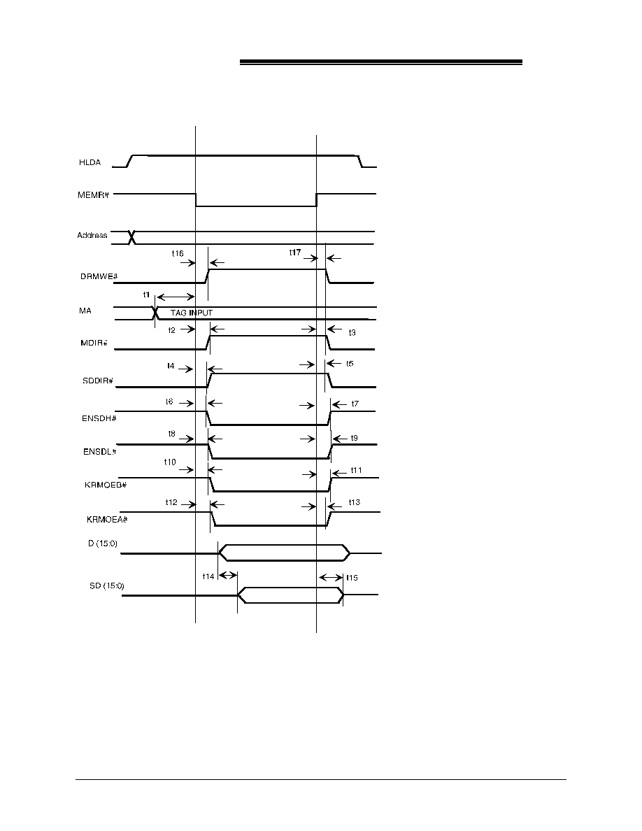
2087
ACC Micro
TM
137
Cache Read Hit in DMA/Master Cycle

2087
ACC Micro
TM
138
AC Specifications
The default load of output signal is 100 pf. The output load which is not 100 pf will specify in load item.
Symbol
Parameter
Min
Typ
Max
Units
t1
MA setup time from MEMR# for internal
comparator
3
9
ns
t2
MDIR# deactivates from MEMR#
3
8
ns
t3
MDIR# activates from #MEMR
3
9
ns
t4
SDDIR# deactivates from #MEMR
5
14
ns
t5
#SDDIR activates from #MEMR
5
15
ns
t6
ENSDH# activates from MEMR#
12
35
ns
t7
ENSDH# deactivates from MEMR#
6
18
ns
t8
ENSDL# activates from MEMR#
12
36
ns
t9
ENSDL# deactivates from MEMR#
6
18
ns
t10
KRMOEB# activates from MEMR#
4
12
ns
t11
KRMOEB# deactivates from MEMR#
3
10
ns
t12
KRMOEA# activates from MEMR#
4
12
ns
t13
KRMOEA# deactivates from MEMR#
3
10
ns
t14
SD delay from D bus
8
23
ns
t15
SD hold time from /MEMR
4
12
ns
t16
DRMWE# deactivates from MEMR#
3
9
ns
t17
DRMWE# activates from MEMR#
3
9
ns
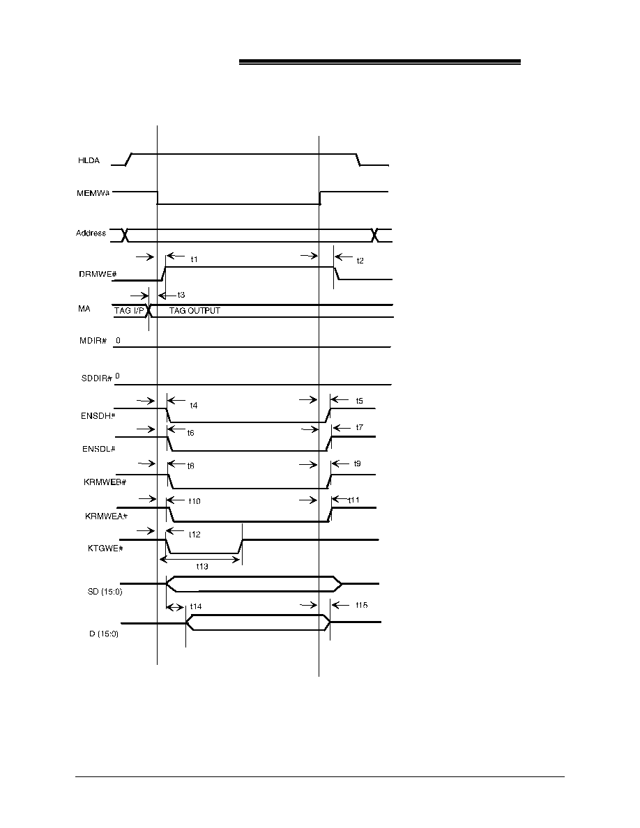
2087
ACC Micro
TM
139
Cache Write Hit in DMA/Master Cycle
2087
ACC Micro
TM
140
AC Specifications
The default load of output signal is 100 pf. The output load which is not 100 pf will specify in load item.
Symbol
Parameter
Min
Typ
Max
Units
t1
DRMWE# deactive from MEMW#
3
9
ns
t2
DRMWE# activate from MEMW#
3
9
ns
t3
MA setup time from MEMW# for internal
comparator
3
9
ns
t4
ENSDH# activate from MEMW#
12
35
ns
t5
ENSDH# deactivate from MEMW#
6
19
ns
t6
ENSDL# activate from MEMW#
12
36
ns
t7
ENSDL# deactivate from MEMW#
6
18
ns
t8
KRMWEB# activate from MEMW#
4
12
ns
t9
KRMWEB# deactivate from MEMW#
3
10
ns
t10
KRMWEA# activate from MEMW#
4
11
ns
t11
KRMWEA# deactivate from MEMW#
3
10
ns
t12
KTGWE# activate from MEMW#
4
13
ns
t13
KTGWE# activate period
60
120
ns
t14
D activate delay from SD
7
20
ns
t15
D hold time from MEMW#
3
10
ns

2087
ACC Micro
TM
141
AT Bus Address Timing
AC Specifications
The default load of output signal is 100 pf. The output load which is not 100 pf will specify in load item.
Symbol
Parameter
Min
Typ
Max
Units
t1
BRDY# activate from CLKI rising edge
5
16
ns
t2
BRDY# deactivate from CLKI rising edge
6
19
ns
t3
BALE activate from CLKI rising edge
7
20
ns
t4
BALE deactivate from SYSCLK rising edge
3
8
ns
t5
SA19 goes high from BALE activate
6
ns
t6
SA19 goes low from BALE activate
10
ns
t7
SA18 goes high from BALE activate
5
ns
t8
SA18 goes low from BALE activate
9
ns
t9
SA17 goes high from BALE activate
4
ns
t10
SA17 goes low from BALE activate
9
ns
t11
SA1 goes high from BALE activate
5
ns
t12
SA1 goes low from BALE activate
9
ns
t13
SBHE# goes high from BALE activate
1
ns
t14
SBHE# goes low from BALE activate
5
ns
t15
SA0 goes high from BALE activate
0
ns
t16
SA0 goes low from BALE activate
2
ns
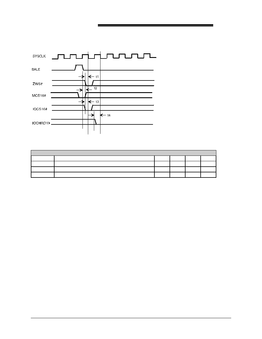
2087
ACC Micro
TM
142
AT Bus Input Timing
AC Specifications
The default load of output signal is 100 pf. The output load which is not 100 pf will specify in load item.
Symbol
Parameter
Min
Typ
Max
Units
t1
ZWS# set tup time to SYSCLK falling edge
0
ns
t2
MCS16# hold time to BALE deactivate
0
ns
t3
IOCS16# setup time to SYSCLK falling edge
0
ns
t4
IOCHRDY# setup time to SYSCLK falling edge
0
ns
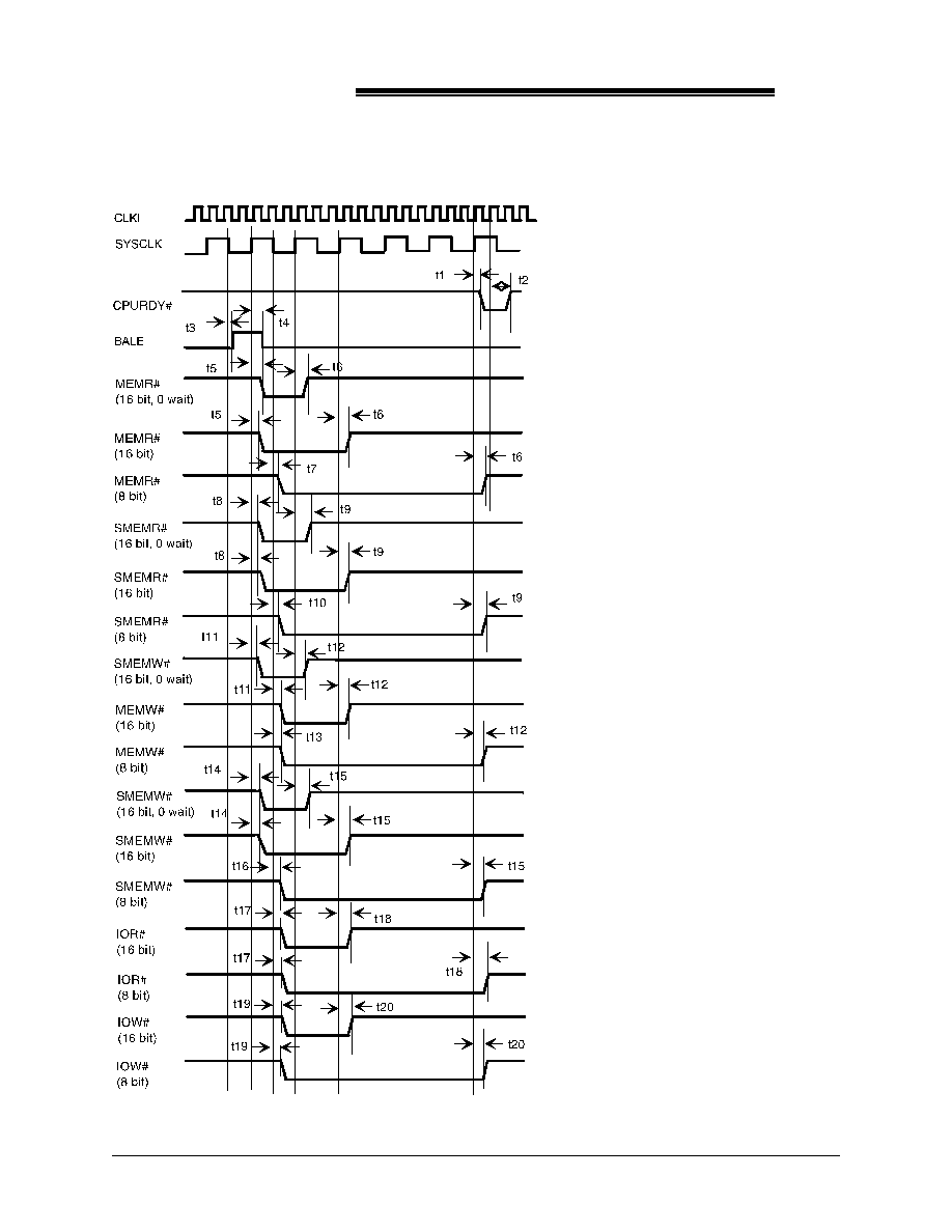
2087
ACC Micro
TM
143
AT Bus Command Timing

2087
ACC Micro
TM
144
AC Specifications
The default load of output signal is 100 pf. The output load which is not 100 pf will specify in load item.
Symbol
Parameter
Min
Typ
Max
Units
t1
CPURDY# activate from CLKI rising edge
5
16
ns
t2
CPURDY# deactivate from CLKI rising edge
7
19
ns
t3
BALE activate from CLKI rising edge
7
20
ns
t4
BALE deactivate from SYSCLK
3
8
ns
t5
MEMR# activate from SYSCLK rising edge
3
14
ns
t6
MEMR# deactivate from SYSCLK rising edge
4
ns
t7
MEMR# activate from SYSCLK falling edge
4
ns
t8
SMEMR# activate from SYSCLK rising edge
30
ns
t9
SMEMR# deactivate from SYSCLK rising edge
16
ns
t10
SMEMR# activate from SYSCLK falling edge
20
ns
t11
MEMW# activate from SYSCLK rising edge
14
ns
t12
#MEMW deactivate from SYSCLK rising edge
4
ns
t13
MEMW# activate from SYSCLK falling edge
4
ns
t14
SMEMW# activate from SYSCLK rising edge
30
ns
t15
SMEMW# deactivate from SYSCLK rising edge
16
ns
t16
SMEMW# activate from SYSCLK falling edge
20
ns
t17
IOR# activate from SYSCLK falling edge
5
ns
t18
IOR# deactivate from SYSCLK rising edge
6
ns
t19
IOW# activate from SYSCLK falling edge
4
ns
t20
IOW# deactivate from SYSCLK rising edge
5
ns
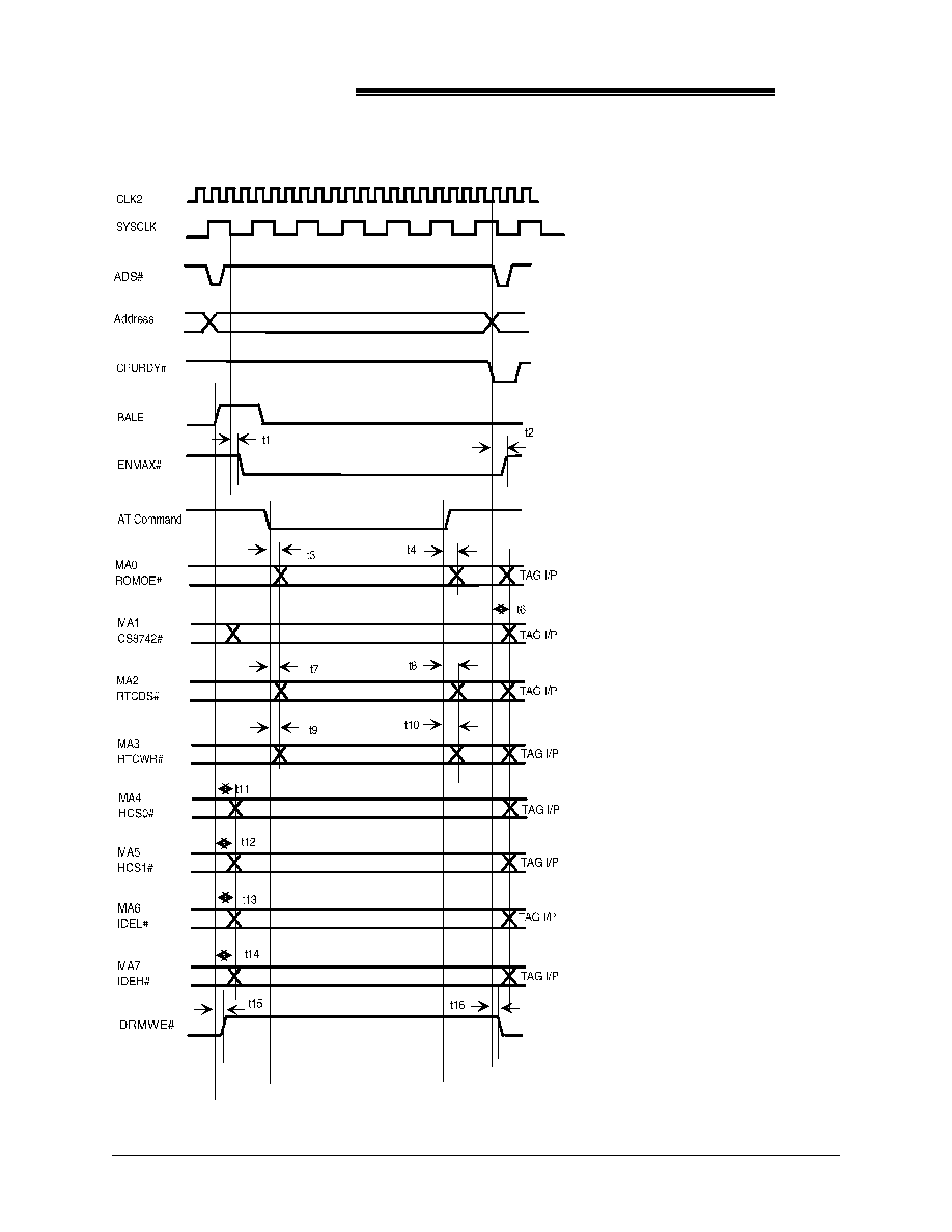
2087
ACC Micro
TM
145
Multiplex Pin Timing
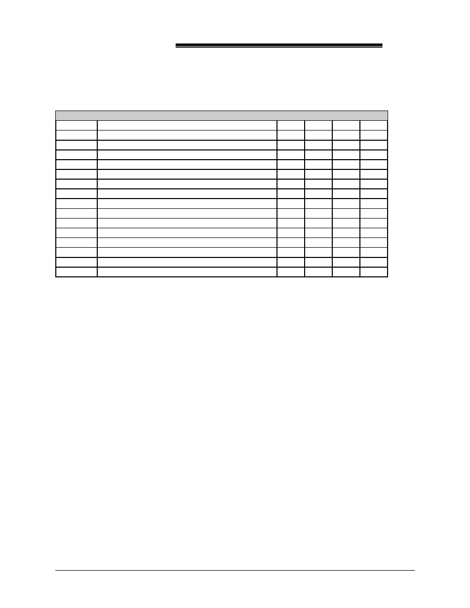
2087
ACC Micro
TM
146
AC Specifications
The default load of output signal is 100 pf. The output load which is not 100 pf will specify in load item.
Symbol
Parameter
Min
Typ
Max
Units
t1
ENMAX# activate from SYSCLK falling edge
13
ns
t2
ENMAX# deactivate from CLKI rising edge
15
ns
t3
ROMOE# activate from MEMR# activate
21
ns
t4
ROMOE# deactivate from MEMR# deactivate
12
ns
t5
CS8742# activate from BALE activate
20
ns
t6
Multiplex output becomes tag INPUT
5
15
ns
t7
RTCDS# activate from IOR# activate
13
ns
t8
RTCDS# deactivate from IOR# deactivate
12
ns
t9
RTCWR# activate from IOW# activate
13
ns
t10
RTCWR# deactivate from IOW# deactivate
11
ns
t11
HCS0# activate from BALE activate
20
ns
t12
HCS1# activate from BALE activate
20
ns
t13
IDEL# activate from BALE activate
20
ns
t14
IDEH# activate from BALE activate
20
ns
t15
DRMWE# activate from CLKI rising edge
4
12
ns
t16
DRMWE# deactivate from CLKI rising edge
ns

2087
ACC Micro
TM
147
Parallel Port FIFO Timing
AC Specifications
The default load of output signal is 100 pf. The output load which is not 100 pf will specify in load item.
Symbol
Parameter
Min
Typ
Max
Units
t1
DATA valid to STROBE# Active
600
ns
t2
STROBE# active pulse width
600
ns
t3
DATA hold from STROBE# inactive
450
ns
t4
STROBE# active to BUSY active
500
ns
t5
BUSY inactive to STROBE# active
680
ns
t6
BUSY inactive to PDATE invalid
80
ns
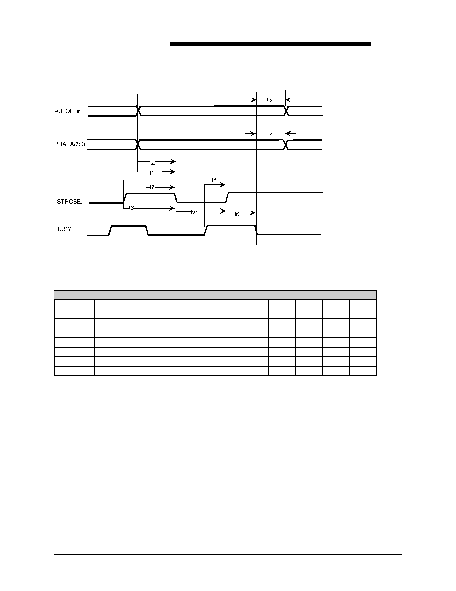
2087
ACC Micro
TM
148
ECP Parallel Port Forward Timing
AC Specifications
The default load of output signal is 100 pf. The output load which is not 100 pf will specify in load item.
Symbol
Parameter
Min
Typ
Max
Units
t1
AUTOFD# valid to STROBE# asserted
0
60
ns
t2
PDATA valid to STROBE# asserted
0
60
ns
t3
BUSY deasserted to AUTOFD# changed
80
180
ns
t4
BUSY deasserted to PDATA changed
80
180
ns
t5
STROBE# asserted to BUSY asserted
0
ns
t6
STROBE# deasserted to busy deasserted
0
ns
t7
BUSY deasserted to STROBE# asserted
80
200
ns
t8
BUSY asserted to STROBE# deasserted
80
180
ns
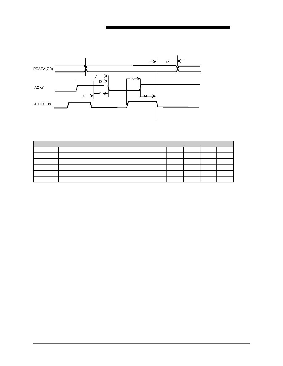
2087
ACC Micro
TM
149
ECP Parallel Port Reverse Timing
AC Specifications
The default load of output signal is 100 pf. The output load which is not 100 pf will specify in load item.
Symbol
Parameter
Min
Typ
Max
Units
t1
PDATA valid to ACK# asserted
0
ns
t2
AUTOFD# deasserted to PDATA changed
0
ns
t3
ACK# asserted to AUTOFD# deasserted
80
200
ns
t4
ACK# deasserted to AUTOFD# asserted
80
200
ns
t5
AUTOFD# asserted to ACK# asserted
0
ns
t6
AUTOFD# deasserted to ACK# deasserted
0
ns

2087
ACC Micro
TM
150
Section 8 2087 Pin Diagram
256-pin PQFP Package

Sales Offices
APPENDIX A-1
ACC Microelectronics Headquarters
ACC Microelectronics Corporation
2500 Augustine Drive,
Santa Clara, CA 95054
Phone: (408) 980-0622
Fax: (408) 980-0626
International Sales
Taiwan
ACC Taiwan Inc.
10-2 FL., No.77. Sec.4,
Nan-King E. Rd.,
Taipei, Taiwan, R.O.C.
Phone: (02) 719-9076
Fax: (02) 514-9127
Seper Technology Corp.
4th Fl., 75 Sec. 3,
Ming-Sheng E. Rd.,
Taipei, Taiwan, R.O.C.
Phone: (02) 506-3320
Fax: (02) 504-8081
Yosun Industrial Corporation
7F, No. 76, Sec. 1, Cheng Kung Road
Nan Kang, Taipei, Taiwan
Phone: (02) 788-1991
Fax: (02) 788-1996
Japan
Nippon IMEX Corp.
1-46-9 Matsubara
Setagaya-Ku
Tokyo, 156 Japan
Phone: (33) 321-8000
Fax: (33) 325-0021
Korea
Intellect, Inc.
Sonam Bldg. 3F, 1001-4,
Dacchi-dong, Kangnam-Ku
Seoul, Korea
Phone: (2) 568-0501
Fax: (2) 558-0444
Connecticut
Dynamic Sales
24 Ray Avenue
Burlington, MA 01803
Phone: (617) 272-5676
Fax: (617) 273-4856
Maine
Dynamic Sales
24 Ray Avenue
Burlington, MA 01803
Phone: (617) 272-5676
Fax: (617) 273-4856
Massachusettes
Dynamic Sales
24 Ray Avenue
Burlington, MA 01803
Phone: (617) 272-5676
Fax: (617) 273-4856
Minnesota
D.A. Case Associates, Inc.
4620 West 77th Street #250
Minneapolis, MN 55435
Phone: (612) 831-6777
Fax: (612) 831-7076
New Hampshire
Dynamic Sales
24 Ray Avenue
Burlington, MA 01803
Phone: (617) 272-5676
Fax: (617) 273-4856
North Dakota
D.A. Case Associates, Inc.
4620 West 77th Street #250
Minneapolis, MN 55435
Phone: (612) 831-6777
Fax: (612) 831-7076

Sales Offices
APPENDIX A-1
contd...
Rhode Island
Dynamic Sales
24 Ray Avenue
Burlington, MA 01803
Phone: (617) 272-5676
Fax: (617) 273-4856
South Dakota
D.A. Case Associates, Inc.
4620 West 77th Street #250
Minneapolis, MN 55435
Phone: (612) 831-6777
Fax: (612) 831-7076
Vermont
Dynamic Sales
24 Ray Avenue
Burlington, MA 01803
Phone: (617) 272-5676
Fax: (617) 273-4856
Wisconsin (Western)
D.A. Case Associates, Inc.
4620 West 77th Street #250
Minneapolis, MN 55435
Phone: (612) 831-6777
Fax: (612) 831-7076