
2016
ACC Microelectronics Corporation, 2500 Augustine Drive, Santa Clara, CA 95054
Phone: (408) 980-0622 Fax: (408) 980-0626
ACC MICRO 2016
BUFFER AND MUX LOGIC
DATA BOOK
MARCH 1997
Revision 2.0

ACC Micro
2016
TM
ACC Microelectronics Corporation, 2500 Augustine Drive, Santa Clara, CA 95054
Phone: (408) 980-0622 Fax: (408) 980-0626
ACC Microelectronics Corporation
2500 Augustine Drive,
Santa Clara, CA 95054
Phone: (408) 980-0622 Fax: (408) 980-0626
Copyright 1996 ACC Microelectronics Corporation. All rights reserved.
P/N 520210
Rev. 2.0
March 1997
Copyright
No part of this publication may be reproduced, transmitted, transcribed, stored in a retrieval system, or
translated into any language or computer language, in any form or by any means, electronic, mechanical,
magnetic, optical, chemical, manual, or otherwise, without the prior written permission of ACC
Microelectronics Corp, 2500 Augustine Drive, Santa Clara, CA 95054.
Disclaimer
ACC Microelectronics Corp. makes no representations or warranties with respect to the design and
documentation herein described and especially disclaims any implied warranties of merchantability or fitness
for any particular purpose. Further, ACC Microelectronics Corp. reserves the right to revise the design and
associated documentation and to make changes from time to time in the content without obligation of ACC
Microelectronics Corp. to notify any person of such revisions or changes.
Trademarks
Single Chip Solution is registered trademark of ACC Microelectronics Corp.
All other trademarks and copyrights are the property of their respective holders.

ACC Micro
2051nt
TM
i
Table of Contents
Title
Page
1.0
Introduction
1
1.1 ACC Micro 2016 Description
1
1.2 ACC Micro 2016 Features
1
1.3 ACC Micro 2016 Block Diagram
2
1.3.1 2016 Internal Block Diagram with 2268/2178/2168/
2056/2057/2066/2048 System Logic
2
1.3.2 2016 Internal Block Diagram with 2086/2087/2089
System Logic
2
1.4 ACC Micro 2016/2178 Application Circuit Diagram
3
2.0
ACC Micro Functional Description
3
3.0
ACC Micro Pin Description
4
3.1 2268/2178/2168/2056/2057/2066/2048 System Logic
4
Table 3.1.1 Address Buffer Signals
4
Table3.1.2 Data Buffer Signals
4
Table 3.1.3 Multiplexer Signals
4
Table 3.1.4 MA Mux Signals
5
Table 3.1.5 AT Bus Signals
5
Table 3.1.6 RESET Signal
5
Table 3.1.7 Power Signals
5
3.2 2086/2087/2089 System Logic
6
Table 3.2.1 Address Buffer Signals
6
Table 3.2.2 Data Buffer Signals
6
Table 3.2.3 Multiplexer Signals
6
Table 3.2.4 MA Mux Signals
6
Table 3.2.5 AT Bus Signals
7
Table 3.2.6 RESET Signal
7
Table 3.2.7 Power Signals
7
4.0
ACC Micro 2016 DC Specifications
8
5.0
ACC Micro 2016 Package Specifications
10
5.1 100-pin PQFP Package Specification
10
5.2 100-pin TQFP Package Specification
11
Appendix A-1 List of Sales Representatives

ACC Micro
2016
TM
1
ACC Micro 2016
Buffer and MUX Logic
Section 1 Introduction
1.1 Description
The ACC Micro 2016 is designed to work together with the system core logic products to provide the decoding
logic for the Real Time Clock (RTC), address buffer, and data buffer for the 486/386DX and Pentium
applications. At least seven TTLs can be saved when using the 2016.
1.2 Features
Address Buffer
Data Buffer
Decode logic for /ROMCS, /KBCS, /RTCWR, and /RTCDS
Saved up to 7 TTLs
100-pin PQFP and TQFP

ACC Micro
2016
TM
2
1.3.1 2016 Internal Block Diagram
with 2268/2178/2168/2056/2057/2066/2048
System Logic
1.3.2 2016 Internal Block Diagram
with 2086/2087/2089 System Logic
245
151
Ax
SAx
IRQx, DRQx
XD
SEL 0,1,2
SD
245 Level Shifter
245
Ax
SAx
D16-23
245 Level Shifter
SA0
SA1
MA0
/IOR
/IOW
AEN
/ROMCS
/KBCS
/RTCWR
/RTCDS
/IENL
/IENH
/HCS0
/HCS1
/RTCDS
/RTCWR
/ROMCS
/KBCS
MUX
0,1,2
DECODER
245
SD0-7
245
SD8-15
XD0-7
D24-31

ACC Micro
2016
TM
3
1.4
2016/2178 Application Circuit Diagram
MA Bus
SA
XD
SD
CPU
Data
Bus
CPU
Address
Bus
DRAMS
EPROM
RTC
SD
CS
573
SRAMS
TAG
Local Bus
Peripheral
Support
ACC Micro
3221
Data
Processor
IDE
Math-
Coprocessor
optional
CPU
IRQx, DRQx
MUX
Power Management
Control Signals
KBC
CS
2 0 1 6
A C C M ic ro
2 1 7 8
/K e y lo c k
Floppy
Serial
Parallel
Section 2 Functional Description
The 2016 can be used with either the 2268/2178/2168/2056/2057/2066/2048 system logic or the
2086/2087/2089 super chip. The 2016 is based on the condition of the /ROMCS signal to determine which
system logic to work with. During power up, if the /ROMCS is pulled high, it works with the
2268/2178/2168/2056/2057/2066/2048 system logic. If /ROMCS is pulled low, it works with the
2086/2087/2089 super chip. The /RTCDS signal (pin 97) requires a pull low through a damping register for all
system logic applications.
ACC Micro
2016
TM
4
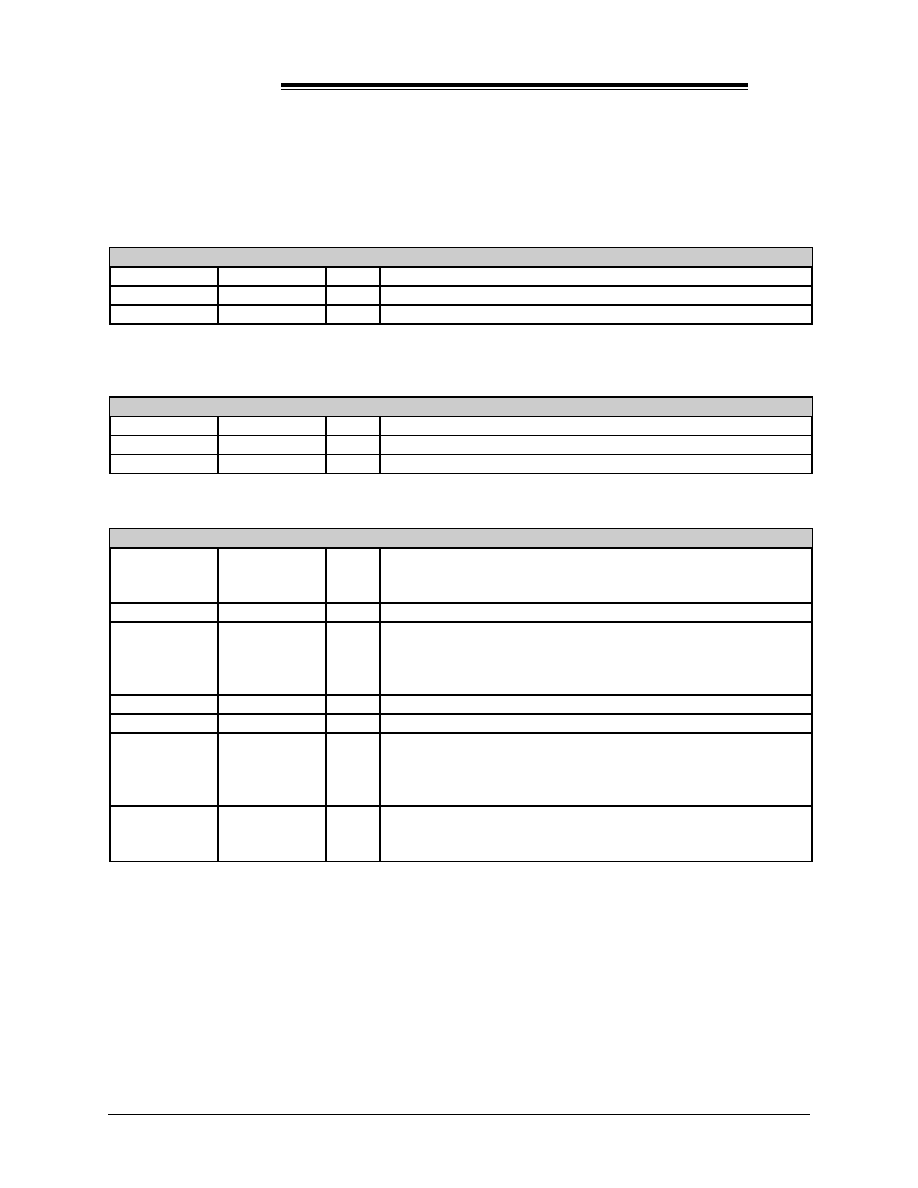
Section 3.0 Pin Description
3.1
2268/2178/2168/2056/2057/2066/2048 System Logic
Table 3.1.1 Address Buffer Signals
Pin Name
Pin #
Type
Description
A2-A16
25--31,33-40
I/O
Local Address Bus
SA2-SA16
6-13,15,17-22
I/O
System Address Bus
/ENABUS
24
I
Address bus buffer
Table 3.1.2 Data Buffer Signals
Pin Name
Pin #
Type
Description
SD0-SD7
73-80
I/O
System Data Bus
XD0-XD7
81-89
I/O
XD Bus
/XDIR
62
I
XD bus direction control
Table 3.1.3 Multiplexer Signals
Pin Name
Pin #
Type
Description
MUXO0-
MUXO2
42-44
O
Multiplexed output for KBINT, IRQ3-9, and /RTCINT.
Multiplexed output for IRQ10-15, KGA20, and /IOCHK.
Multiplexed output for DRQ0-3, DRQ5-7, and /KBRST.
SEL0-SEL2
45-47
I
Multiplexer select pins for MUXO0-MUXO2.
IRQ3-IRQ7
IRQ9,
/RTCINT
IRQ10-IRQ13
48-52
53
55
56-58
I
RTC interrupt.
DRQ6-7
59-60
I
DMA request.
/KBCS
61
O
Keyboard chip select.
IRQ14-IRQ15
/IOCHK
DRQ0-DRQ3
DRQ5
63-64
65
66-68, 71
72
I
Interrupt
/IOCHK
DRQ0-DRQ3
DRQ5
65
66-68, 71
72
I
I/O channel check DMA request.

ACC Micro
2016
TM
5
Table 3.1.4 MA Mux Signals
Pin Name
Pin #
Type
Description
MA0
23
I
MA0 from ACC Micro system logic. In AT cycle, this is a
multiplexed pin for /ROMCS.
/ROMCS
92
I/O
ROM Chip Select output. Pulled high.
/RTCWR
96
O
RTC Write output.
/RTCDS
97
I/O
RTC Data Strobe output.
/KGA20
2
I/O
Keyboard GA20 input
/KBRST
3
I/O
Keyboard reset input.
KBINT
98
I/O
Keyboard interrupt input.
IRQ12
99
I/O
Interrupt request.
Table 3.1.5 AT Bus Signals
Pin Name
Pin #
Type
Description
/IOR
93
I
AT Bus Read.
/IOW
94
I
AT Bus Write.
AEN
95
I
Bus Hold Acknowledge
/MASTER
100
I
AT Bus Master
/REF
1
I
Refresh Cycle.
SA0
4
I
System Address Bit 0.
SA1
5
I
System Address Bit 1.
Table 3.1.6 RESET Signal
Pin Name
Pin #
Type
Description
/RST
91
I
Chip reset.
Table 3.1.7 Power Signals
Pin Name
Pin #
Type
Description
VDD
16, 32, 54, 69,
90
P
5V power.
GND
14, 41, 70, 88
P
Ground.

ACC Micro
2016
TM
6
3.2
2086/2087/2089 System Logic
Table 3.2.1 Address Buffer Signals
Pin Name
Pin #
Type
Description
A2-A16
25--31,33-40
I/O
Local Address Bus
SA2-SA16
6-13,15,17-22
I/O
System Address Bus
/ENABUS
24
I
Address bus buffer
Table 3.2.2 Data Buffer Signals
Pin Name
Pin #
Type
Description
SD0-SD7
73-80
I/O
System Data Bus
XD0-XD7
81-89
I/O
XD Bus
/XDIR
62
I
XD bus direction control
Table 3.2.3 Multiplexer Signals
Pin Name
Pin #
Type
Description
D16-D31
42-53, 55-58
I/O
CPU Data Bus.
/ENSDL
59
I
SD Bus buffer low byte enable.
/ENSDH
60
I
SD Bus buffer high byte enable.
/SDDIR
61
I/O
SD Bus Direction control.
SD8-SD15
63-68, 71-72
I/O
System data bus.
Table 3.2.4 MA Mux Signals
Pin Name
Pin #
Type
Description
MA0
23
I
MA0 from ACC Micro system logic. In AT cycle, this is a
multiplexed pin for /ROMCS.
/ROMCS
92
I/O
ROM Chip Select output. Pulled low.
/RTCWR
96
O
RTC Write output.
/RTCDS
97
I/O
RTC Data Strobe output.
/IENL
2
I/O
IDE data buffer low byte enable.
/IENH
3
I/O
IDE data buffer high byte enable.
/HCS0
98
I/O
IDE chip select bit 0.
/HCS1
99
I/O
IDE chip select bit 1.

ACC Micro
2016
TM
7
Table 3.2.5 AT Bus Signals
Pin Name
Pin #
Type
Description
/IOR
93
I
AT Bus Read.
/IOW
94
I
AT Bus Write.
AEN
95
I
Bus Hold Acknowledge
/MASTER
100
I
AT Bus Master
/REF
1
I
Refresh Cycle.
SA0
4
I
System Address Bit 0.
SA1
5
I
System Address Bit 1.
Table 3.2.6 RESET Signal
Pin Name
Pin #
Type
Description
/RST
91
I
Chip reset.
Table 3.2.7 Power Signals
Pin Name
Pin #
Type
Description
VDD
16, 32, 54, 69,
90
P
5V power.
GND
14, 41, 70, 88
P
Ground.

ACC Micro
2016
TM
8
Section 4.0
2016 DC Specifications
TA = 0� C to 45� C, Vdd = 5.0V � 5%
Signals:
AEN, MA0, SA0, SA1, /ENABUS, /IOR, /IOW, /REF, /MASTER, /XDIR, DRQ6, DRQ7
Parameter
Sym.
Min.
Max.
Unit
Test Condition
Input low voltage
VIL
0.8
V
Vdd = 5.0 � 5%
Input high voltage
VIH
2.0
V
Vdd = 5.0 � 5%
Input low current
IIL
-10.0
uA
Vin = 0.0V
Input high current
IIH
10.0
uA
Vin = Vdd
Signals: /RST
Parameter
Sym.
Min.
Max.
Unit
Test Condition
Threshold voltage low to high
VTLH
2.4
3.0
V
Vdd = 5.0V �
5%
Threshold voltage high to low
VTLH
1.2
1.8
V
Vdd = 5.0V �
5%
Hysteresis
VH
0.9
1.5
V
Triput low Leakage Current
IIL
-10.0
uA
Vin = 0.0V
Input high Leakage Current
IIH
10.0
uA
Vin = 5.5V
Signals: /RTC
Parameter
Sym.
Min.
Max.
Unit
Test Condition
Output low voltage
VOL
0.4
V
IOL = 4.0 mA
Output high voltage
VOH
2.4
V
IOH = 4.0 mA
Tristate Output Leakage
Current
IOZ
-10.0
10.0
uA
0V < Vout < Vdd
Signals:
A2-A16, MUX0-MUX2, SEL0-SEL2, IRQ3-IRQ7, IRQ9-IRQ13, /RTCINT, XD0-XD7,
/ROMCS,
/RTCDS, /KBCS
Parameter
Sym.
Min.
Max.
Unit
Test Condition
Input low voltage
VTL
0.8
V
Vdd = 5.0V � 5%
Input high voltage
VIH
2.0
V
Vdd = 5.0V � 5%
Input low current
IIL
-10.0
uA
VIN = 0.0V
Input high current
IIH
10.0
uA
VIN = Vdd
Output low voltage
VOL
0.4
V
IOL = 4.0 mA
Output high voltage
VOH
2.4
V
IOH = -4.0 mA
Tristate output leakage current
IOZ
-10.0
10.0
uA
0V < Vout < Vdd

ACC Micro
2016
TM
9
Signals: KBINT, /KGA20, /KBRST
Parameter
Sym.
Min.
Max.
Unit
Test Condition
Input low voltage
VTL
0.8
V
Vdd = 5.0 V � 5%
Input high voltage
VIH
2.0
V
Vdd = 5.0 V � 5%
Input low current
IIL
-10.0
uA
VIN = 0.0V
Input high current
IIH
10.0
uA
VIN = Vdd
Output low voltage
VOL
0.4
V
IOL = 4.0 mA
Output high voltage
VOH
2.4
V
IOH = -4.0 mA
Tristate output leakage current
IOZ
-10.0
10.0
uA
0V < Vout < Vdd
Signals: SA2-SA16, SD0-SD7
Parameter
Sym.
Min.
Max.
Unit
Test Condition
Input low voltage
VIL
0.8
V
Vdd = 5.0V � 5%
Input high voltage
VIH
2.0
V
Vdd = 5.0V � 5%
Input low current
IIL
-10.0
uA
VIN = 0.0V
Input high current
IIH
10.0
uA
VIN = Vdd
Output low voltage
VOL
0.4
V
IOL = 4.0 mA
Output high voltage
VOH
2.4
V
IOH = -4.0 mA
Tristate output leakage current
IOZ
-10.0
10.0
uA
0V < Vout < Vdd
Signals: IRQ14, IRQ15, /IOCHK, DRQ0-DRQ3, DRQ5
Parameter
Sym.
Min.
Max.
Unit
Test Condition
Input low voltage
VIL
0.8
V
Vdd = 5.0V � 5%
Input high voltage
VIH
2.0
V
Vdd = 5.0V � 5%
Input low current
IIL
-10.0
uA
VIN = 0.0V
Input high current
IIH
10.0
uA
VIN = Vdd
Output low voltage
VOL
0.4
V
IOL = 4.0 mA
Output high voltage
VOH
2.4
V
IOH = -4.0 mA
Tristate output leakage current
IOZ
-10.0
10.0
uA
0V < Vout < Vdd

ACC Micro
2016
TM
10
Section 5
Package Specifications
5.1
100-pin PQFP Package Specification
Unit:
inches (mms.)
1
100
81
80
51
50
31
30
0-7�
.547-.555
(13.9-14.1)
.008-.016
(.20-.40)
.919-.939
(23.35-23.85)
.783-.791 (19.9-20.1)
.683-.703
(17.35-17.85)
.026 (0.65)
.101-.118 (2.57-3.00)
.071 (1.80)
.020-.037
(.50-.95)
.004-.008
(.10-.20)
.002-.02 (.05-.50)

ACC Micro
2016
TM
11
5.2
100-pin TQFP Package Specification
Unit:
inches (mms.)
1
100
76
75
51
50
26
25
0-7�
.547-.555
(13.9-14.1)
.007-.011
(.17-.27)
.626-.634
(15.9-16.1)
.547-.555 (13.9-14.1)
.626-.634
(15.9-16.1)
.(0.50)
.053-.057 (1.35-1.45)
.039 (1.0)
.018-.030
(.45 - .75)
.004-.008
(.09-.20)
.002-.006 (.05-.15)

Sales Offices
APPENDIX A-1
ACC Microelectronics Headquarters
ACC Microelectronics Corporation
2500 Augustine Drive,
Santa Clara, CA 95054
Phone: (408) 980-0622
Fax: (408) 980-0626
International Sales
Taiwan
ACC Taiwan Inc.
10-2 FL., No.77. Sec.4,
Nan-King E. Rd.,
Taipei, Taiwan, R.O.C.
Phone: (02) 719-9076
Fax: (02) 514-9127
Seper Technology Corp.
4th Fl., 75 Sec. 3,
Ming-Sheng E. Rd.,
Taipei, Taiwan, R.O.C.
Phone: (02) 506-3320
Fax: (02) 504-8081
Yosun Industrial Corporation
7F, No. 76, Sec. 1, Cheng Kung Road
Nan Kang, Taipei, Taiwan
Phone: (02) 788-1991
Fax: (02) 788-1996
Japan
Nippon IMEX Corp.
1-46-9 Matsubara
Setagaya-Ku
Tokyo, 156 Japan
Phone: (33) 321-8000
Fax: (33) 325-0021
Korea
Intellect, Inc.
Sonam Bldg. 3F, 1001-4,
Dacchi-dong, Kangnam-Ku
Seoul, Korea
Phone: (2) 568-0501
Fax: (2) 558-0444
Connecticut
Dynamic Sales
24 Ray Avenue
Burlington, MA 01803
Phone: (617) 272-5676
Fax: (617) 273-4856
Maine
Dynamic Sales
24 Ray Avenue
Burlington, MA 01803
Phone: (617) 272-5676
Fax: (617) 273-4856
Massachusettes
Dynamic Sales
24 Ray Avenue
Burlington, MA 01803
Phone: (617) 272-5676
Fax: (617) 273-4856
Minnesota
D.A. Case Associates, Inc.
4620 West 77th Street #250
Minneapolis, MN 55435
Phone: (612) 831-6777
Fax: (612) 831-7076
New Hampshire
Dynamic Sales
24 Ray Avenue
Burlington, MA 01803
Phone: (617) 272-5676
Fax: (617) 273-4856
North Dakota
D.A. Case Associates, Inc.
4620 West 77th Street #250
Minneapolis, MN 55435
Phone: (612) 831-6777
Fax: (612) 831-7076

Sales Offices
APPENDIX A-1
contd...
Rhode Island
Dynamic Sales
24 Ray Avenue
Burlington, MA 01803
Phone: (617) 272-5676
Fax: (617) 273-4856
South Dakota
D.A. Case Associates, Inc.
4620 West 77th Street #250
Minneapolis, MN 55435
Phone: (612) 831-6777
Fax: (612) 831-7076
Vermont
Dynamic Sales
24 Ray Avenue
Burlington, MA 01803
Phone: (617) 272-5676
Fax: (617) 273-4856
Wisconsin (Western)
D.A. Case Associates, Inc.
4620 West 77th Street #250
Minneapolis, MN 55435
Phone: (612) 831-6777
Fax: (612) 831-7076