! !
"
4/7
& + ,-+#-
)
%
Pin Name
Type
Pin
No.
Drive
(mA)
Functions
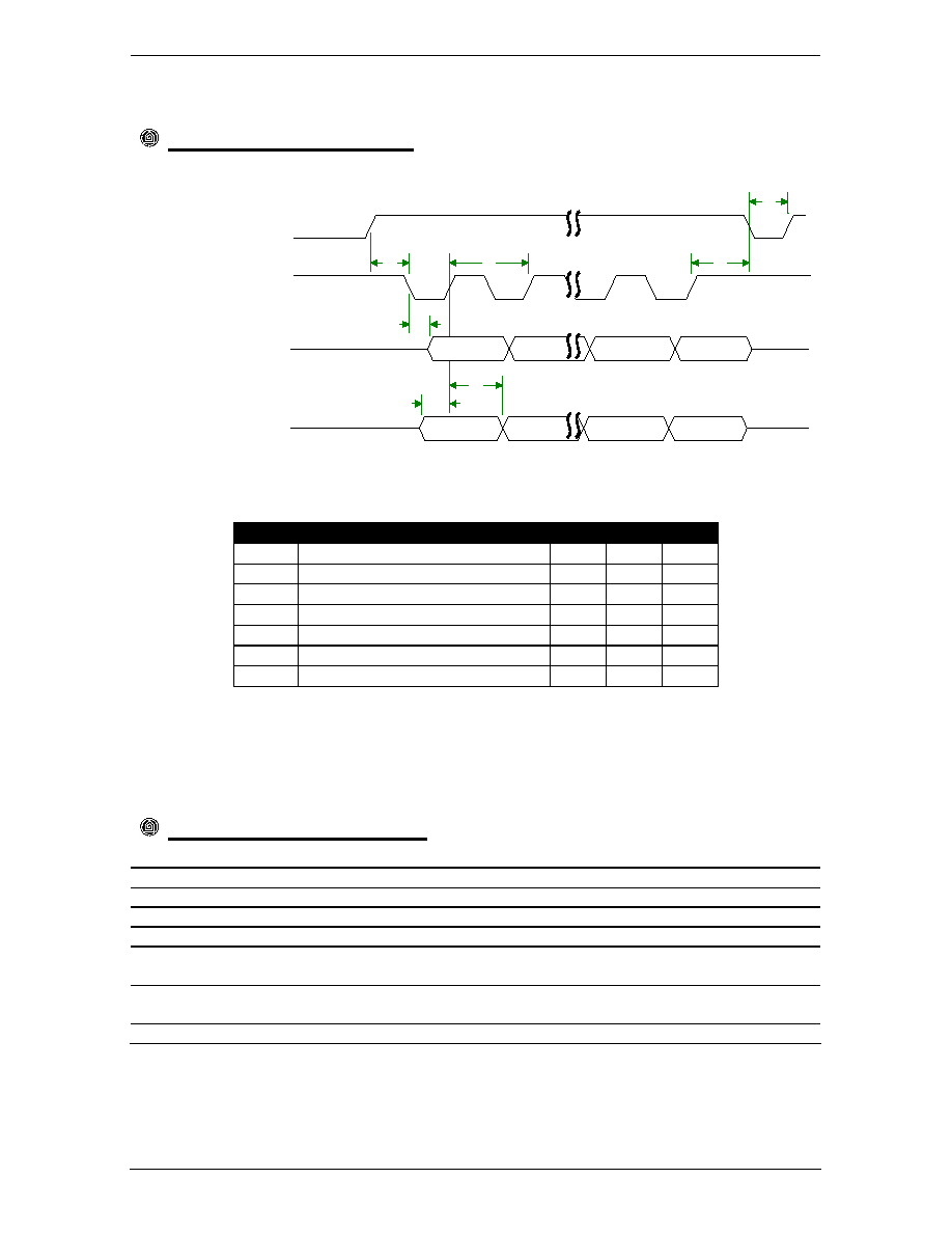
CK
Output
1
1
Frequency carrier = OSCI/XDVI.
HCK
Output
2
1
OSCI clock output.
INT
2
Output
3
2
Interrupt.
HSK
2
Tri-state
4
2
Handshake signal.
VDDCORE
VCC
5,27
-
3.3V input.
VSSOUT
GND
6,30
-
Ground signal.
OSCI
Input
7
-
Input clock signal.
VDDOUT
VCC
8,28
-
3.3V input.
VSSCORE
GND
9,31
-
Ground signal.
PORT0
1,2
Inout
10
2
Data IO 0 / Data available on the communication port.
PORT1
1,2
Inout
11
2
Data IO 1 / Line busy indication.
PORT2
1,2
Inout
12
2
Data IO 2 / Communication port busy indication.
PORT3
1,2
Inout
13
2
Data IO 3 / Serial data in (SDI).
PORT4
1,2
Inout
14
2
Data IO 4 / Serial data out (SDO).
PORT5
1,2
Input
15
-
Clock polarity in serial mode / read-write enable in parallel
mode. Read = 1'b1.
PORT6
1,2
Input
16
-
Strobe or clock signal.
PORT7
1,2
Input
17
-
Chip Select.
POEN3
2
Output
18
2
Port output enable for PORT3. Output when POEN3 = 1.
POEN4
2
Output
19
2
Port output enable for PORT0, 1, 2 and 4. Output when
POEN4 = 1.
PORTYPE
1,2
Input
20
-
Communication port type. 1 = Parallel, 0 = serial.
CSPOL
1,2
Input
21
-
Chip Select polarity. 1 = CS active high.
RCVNG
Output
22
8
Receiving a valid packet. Can drive a LED. Active low.
XING
Output
23
8
Transmitting a valid packet. Can drive a LED. Active low.
IN
2
Input
24
-
Receiver input.
XOUT
2
Output
25
1
Transmitter output. Need to be filtered to eliminate second
frequency generated by the chip.
XOUTE
2
Output
26
1
Amplifier enable signal.
RESET
Output
29
-
Hardware reset. Active low. Internal pull-up.
CNFGD
Output
32
-
Configuration status. Active high. Can drive a LED.
SCAN_EN
3
Input
33
-
Use to internal test. Internal pull-down. Must be tied to GND.
RBURSTP
Output
34
1
DEBUG pin. Receiver burst pulse. No connect.
RSOPP
Output
35
1
DEBUG pin. Receiver side. Start of packet pulse. No connect.
REOF
Output
36
1
DEBUG pin. Receiver side. End of field. No connect.
REOP
Output
37
1
DEBUG pin. Receiver side. End of packet. No connect.
RBIT
Output
38
1
DEBUG pin. Receiver side. A bit of a packet.
RBITSTR
Output
39
1
DEBUG pin. Receiver side. Strobe to validate a RBIT.
LBUSY
Output
40
1
DEBUG pin. Line busy indicator.
XBITOUT
Output
41
1
DEBUG pin. TX side. Output bit before modulation.
XBITSTR
Output
42
1
DEBUG pin. TX side. Output bit strobe.
XCMD
Output
43
1
DEBUG pin. TX side. Command indicator.
TESTMODE
Output
44
1
Use by BIST test. Internal pull-down. Must be tied to GND.
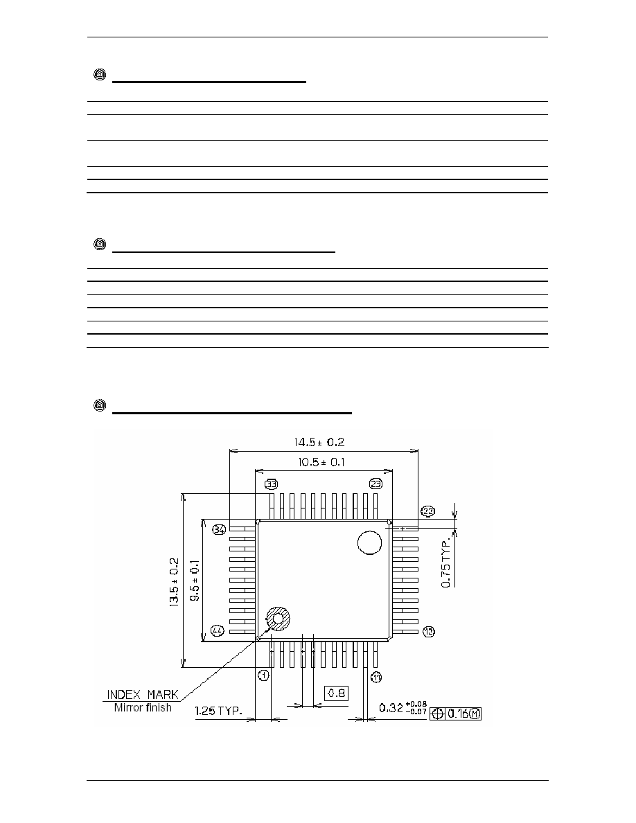
#$ * $! ! * "!
*
* ,542 $"
#$ *
5 #
!
#$ * $! ! * "!
*
+