
Rev.1
Page 1
ASCEND
Semiconductor
4Mx4 EDO
Data sheet

Rev.1
Page 2
AD 40 4M 4 2 V S A ≠ 5
Ascend
Semiconductor
EDO/FPM
: 40
D-RAMBUS
: 41
DDRSDRAM
: 42
DDRSGRAM
: 43
SGRAM
: 46
SDRAM
: 48
Density
16M : 16 Mega Bits
8M : 8 Mega Bits
4M : 4 Mega Bits
2M : 2 Mega Bits
1M : 1 Mega Bit
Package
Organization
4: x4
8 : x8
9 : x9
16 : x16
18 : x18
32 : x32
Revision
A : 1st B : 2nd
C : 3rd D :4th
Min Cycle Time ( Max Freq.)
-5 : 5ns ( 200MHz )
-6 : 6ns ( 167MHz )
-7 : 7ns ( 143MHz )
-75 : 7.5ns ( 133MHz )
-8 : 8ns ( 125MHz )
-10 : 10ns ( 100MHz )
EDO : -5 (50 ns)
-6 (60 ns)
Interface
V: 3.3V
R: 2.5V
C: CSP B: uBGA
T: TSOP Q: TQFP
P: PQFP ( QFP )
L: LQFP S: SOJ
Refresh
1 : 1K 8 : 8K
2 : 2K 6 :16K
4 : 4K

Rev.1
Page 3
Description
The device CMOS Dynamic RAM organized as 4,194,304 words x 4 bits with extended data out access
mode. It is fabricated with an advanced submicron CMOS technology and designed to operate from a single
3.3V oniy power supply. Low voltage operation is more suitable to be used on battery backup, portable elec-
tronic application. lt is packaged in JEDEC standard 26/24-pin plastic SOJ or TSOP(II).
Features
∑ Single 3.3V(
%) only power supply
∑ High speed t
RAC
acess time: 50/60ns
∑ Low power dissipation
- Active mode : 432/396 mW (Mas)
- Standby mode: 0.54 mW (Mas)
∑ Extended - data - out(EDO) page mode access
∑ I/O level: CMOS level (Vcc = 3.3V)
∑ 2048 refresh cycle in 32 ms(Std.) or 128 ms(S-version)
∑ 4 refresh modesh:
- RAS only refresh
- CAS - before - RAS refresh
- Hidden refresh
- Self-refresh(S-version)
10
±
Rev.1
Page 4
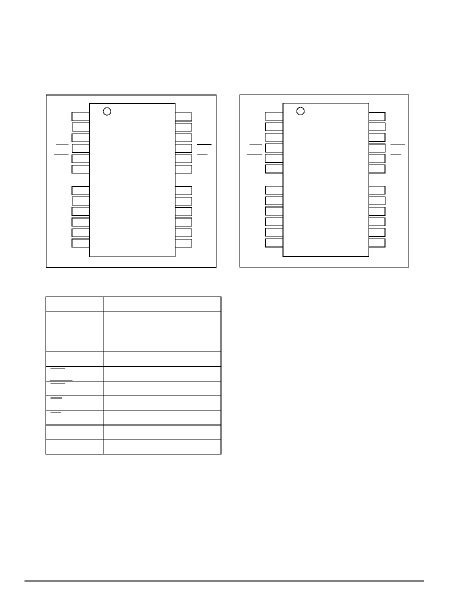
Pin Name
Function
A0-A10
Address inputs
- Row address
- Column address
- Refresh address
DQ1~DQ4
Data-in / data-out
RAS
Row address strobe
CAS
Column address strobe
WE
Write enable
OE
Output enable
Vcc
Power (+ 3.3V)
Vss
Ground
VCC
1
DQ1
2
DQ2
3
DQ3
4
DQ4
5
VCC
6
8
9
10
11
NC
12
WE
13
A0
A1
17
A2
18
A3
19
VSS
RAS
CAS
OE
A8
A7
A6
A5
A4
VSS
A
D
4
0
4
M
4
2
V
S
Pin Description
Pin Configuration
21
22
23
24
25
26
15
14
16
A10
26/24-PIN 300mil Plastic SOJ
A9
VCC
1
DQ1
2
DQ2
3
DQ3
4
DQ4
5
VCC
6
8
9
10
11
NC
12
WE
13
A0
A1
17
A2
18
A3
19
VSS
RAS
CAS
OE
A8
A7
A6
A5
A4
VSS
A
D
4
0
4
M
4
2
V
T
21
22
23
24
25
26
15
14
16
A10
26/24-PIN 300mil Plastic TSOP (ll)
A9
A0-A10
A0-A10
A0-A10
Rev.1
Page 5
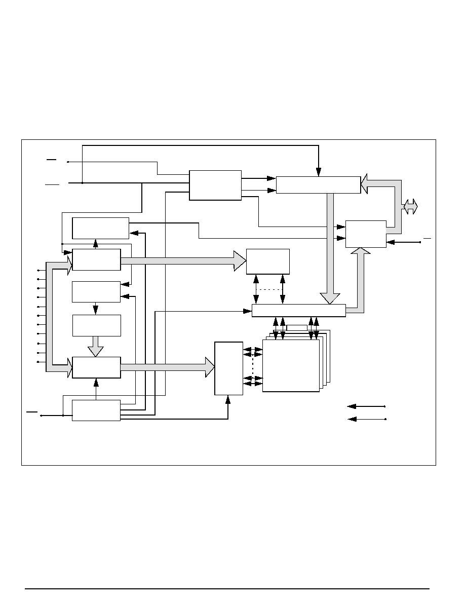
WE
CAS
NO. 2 CLOCK
GENERATOR
COLUMN
ADDRESS
BUFFERS (11)
REFRESH
CONTROLLER
REFRESH
COUNTER
BUFFERS (11)
ADDRESS
ROW
NO. 1 CLOCK
GENERATOR
A0
RAS
A1
A2
A3
A4
A5
A6
A7
A8
CONTROL
LOGIC
DATA-IN BUFFER
DATA-OUT
BUFFER
OE
DQ1
.
DQ4
.
COLUMN
DECODER
2048
SENSE AMPLIFIERS
I/O GATING
2048x4
2048x2048x4
MEMORY
ARRAY
2
0
4
8
R
O
W
D
E
C
O
D
E
R
Vcc
Vss
Block Diagram
A9
A10

Rev.1
Page 6
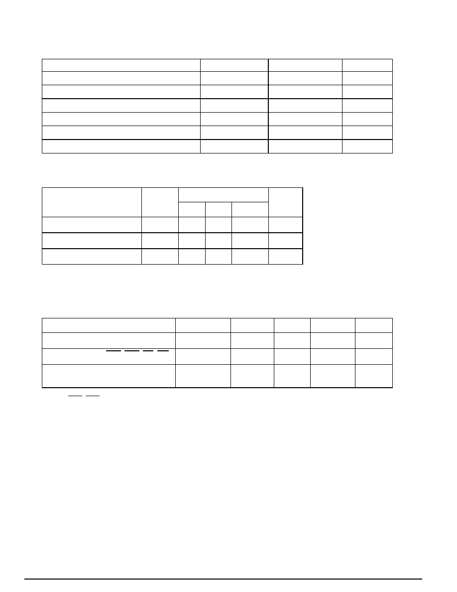
TRUTH TABLE
Notes: 1. EARLY WRITE only.
FUNCTION
RAS
CAS
WE
OE
ADDRESSES
DQ
S
Notes
ROW
COL
STANDBY
H
X
X
X
X
High-Z
READ
L
L
H
L
ROW
COL
Data-Out
WRITE: (EARLY WRITE )
L
L
L
X
ROW
COL
Data-ln
READ WRITE
L
L
ROW
COL
Data-Out,Data-ln
EDO-PAGE-
MODE READ
1st Cycle
L
H
L
ROW
COL
Data-Out
2nd Cycle
L
H
L
n/a
COL
Data-Out
EDO-PAGE
MODE WRITE
1st Cycle
L
L
X
ROW
COL
Data-In
2nd Cycle
L
L
X
n/a
COL
Data-In
EDO-
PAGE-MODE
READ-WRITE
1st Cycle
L
ROW
COL
Data-Out, Data-In
2nd Cycle
L
n/a
COL
Data-Out, Data-In
HIDDEN
REFRESH
READ
L
H
L
ROW
COL
Data-Out
WRITE
L
L
X
ROW
COL
Data-In
1
RAS-ONLY REFRESH
L
H
X
X
ROW
n/a
High-Z
CBR REFRESH
L
H
X
X
X
High-Z
H
X
H
L
L
H
H
L
H
L
H
L
H
L
H
L
H
L
L
H
H
L
H
L
L
H
L
H
L
L
H
L
H
L
Rev.1
Page 7
Absolute Maximum Ratings
Recommended DC Operating Conditions
Capacitance
Ta = 25∞C, V
CC
= 3.3V
%, f = 1MHz
Note: 1. Capacitance measured with effective capacitance measuring method.
2. RAS, CAS = V
IH
to disable Dout.
Parameter
Symbol
Value
Unit
Voltage on any pin relative to Vss
V
T
-0.5 to + 4.6
V
Supply voltage relative to Vss
V
CC
-0.5 to + 4.6
V
Short circuit output current
I
OUT
50
mA
Power dissipation
P
D
1.0
W
Operating temperature
T
OPT
0 to + 70
∞C
Storage temperature
T
STG
-55 to + 125
∞C
Parameter/Condition
Symbol
3.3 Volt Version
Unit
Min
Typ
Max
Supply Voltage
V
CC
3.0
3.3
3.6
V
Input High Voltage, all inputs
V
IH
2.0
- V
CC
+ 0.3
V
Input Low Voltage, all inputs
V
IL
-0.3
-
0.8
V
Parameter
Symbol
Typ
Max
Unit
Note
Input capacitance (Address)
C
I1
-
5
pF
1
Input capacitance (RAS, CAS, OE, WE)
C
I2
-
7
pF
1
Output capacitance
(Data-in, Data-out)
C
I/O
-
7
pF
1, 2
10
±
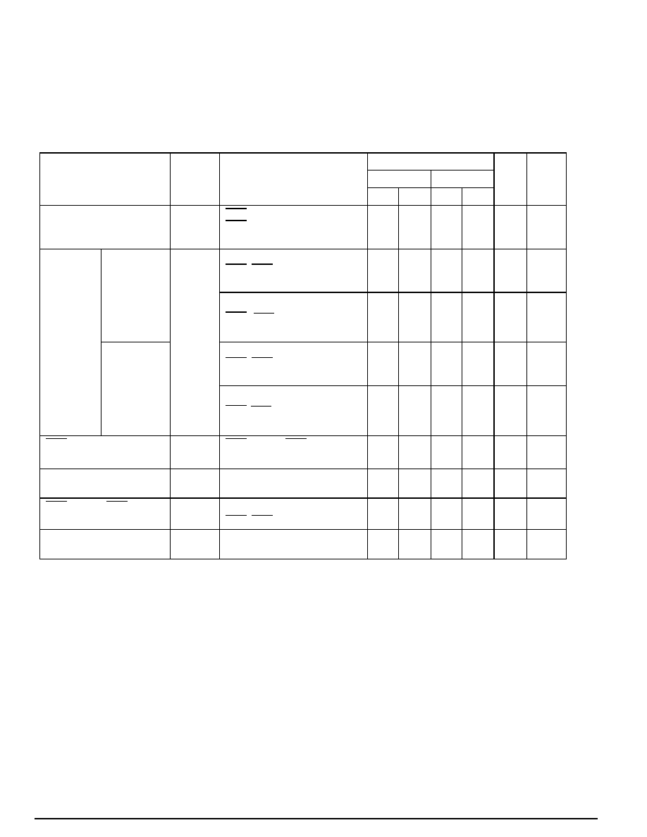
Rev.1
Page 8
DC Characteristics :
(T
a
= 0 to 70∞C
,
V
CC
= + 3.3V
%, V
SS
= 0V)
Parameter
Symbol
Test Conditions
AD404M42V
Unit
Notes
-5
-6
Min
Max
Min
Max
Operating current
I
CC1
RAS cycling
CAS, cycling
t
RC
= min
-
120
-
110
mA
1, 2
Standby
Current
Low
power
S-version
I
CC2
LVTTL interface
RAS, CAS = V
IH
Dout = High-Z
-
0.5
-
0.5
mA
CMOS interface
RAS, -0.2V
Dout = High-Z
-
0.15
-
0.15
mA
Standard
power
version
LVTTL interface
RAS, CAS = V
IH
Dout = High-Z
-
2
-
2
mA
CMOS interface
RAS,
-0.2V
Dout = High-Z
-
0.5
-
0.5
mA
RAS- only refresh current
I
CC3
RAS cycling, CAS = V
IH
t
RC
= min
-
120
-
110
mA
1, 2
EDO page mode current
I
CC4
t
PC
= min
-
90
-
80
mA
1, 3
CAS- before- RAS refresh
current
I
CC5
t
RC
= min
RAS, CAS cycling
-
120
-
110
mA
1, 2
Self- refresh current
(S-Version)
I
CC8
- 550 - 550
10
±
CAS
V
C C
CAS
V
C C
t
RASS
100
µ
s
µ
A
Rev.1
Page 9
DC Characteristics :
(T
a
= 0 to 70∞C
,
V
CC
= +3.3V
%, V
SS
= 0V)
Notes:
1. I
CC
is specified as an average current. It depends on output loading condition and cycle rate when the
device is selected. I
CC
max is specified at the output open condition.
2. Address can be changed once or less while RAS = V
IL
.
3. For I
CC4
, address can be changed once or less within one EDO page mode cycle time.
Parameter
Symbol
Test Conditions
AD404M42V
Unit
Notes
-5
-6
Min
Max
Min
Max
Input leakage current
I
LI
+ 0.3V
-5
5
-5
5
Output leakage current
I
LO
+ 0.3V
Dout = Disable
-5
5
-5
5
Output high Voltage
V
OH
I
OH
= -2mA
2.4
-
2.4
-
V
Output low voltage
V
OL
I
OL
= +2mA
-
0.4
-
0.4
V
10
±
0V
Vin
V
C C
µ
A
0V
Vout
V
CC
µ
A
Rev.1
Page 10
AC Characteristics
(
T
a
= 0 to + 70
∞C
, V
cc
= 3.3V %, V
ss
= 0V) *1, *2, *3, *4
Test conditions
∑ Output load: one TTL Load and 100pF (V
CC
= 3.3V
%)
∑ Input timing reference levels:
V
IH
= 2.0V, V
IL
= 0.8V (V
CC
= 3.3V
%)
∑ Output timing reference levels:
V
OH
= 2.0V, V
OL
= 0.8V
10
±
10
±
10
±
Read, Write, Read- Modify- Write and Refresh Cycles
(Common Parameters)
Parameter
Symbol
AD404M42V
Unit
Notes
-5
-6
Min
Max
Min
Max
Random read or write cycle time
t
RC
84
-
104
-
ns
RAS precharge time
t
RP
30
-
40
-
ns
CAS precharge time in normal mode
t
CPN
10
-
10
-
ns
RAS pulse width
t
RAS
50
10000
60
10000
ns
5
CAS pulse width
t
CAS
8
10000
10
10000
ns
6
Row address setup time
t
ASR
0
-
0
-
ns
Row address hold time
t
RAH
8
-
10
-
ns
Column address setup time
t
ASC
0
-
0
-
ns
7
Column address hold time
t
CAH
8
-
10
-
ns
RAS to CAS delay time
t
RCD
12
37
14
45
ns
8
RAS to column address delay time
t
RAD
10
25
12
30
ns
9
Column address to RAS lead time
t
RAL
25
-
30
-
ns
RAS hold time
t
RSH
8
-
10
-
ns
CAS hold time
t
CSH
38
-
40
-
ns
CAS to RAS precharge time
t
CRP
5
-
5
-
ns
10
OE to Din delay time
t
OED
12
-
15
-
ns
Transition time (rise and fall)
t
T
1
50
1
50
ns
11
Refresh period
t
REF
-
32
-
32
ms
Refresh period (S- Version)
t
REF
-
128
-
128
ms
CAS to output in Low- Z
t
CLZ
0
-
0
-
ns
CAS delay time from Din
t
DZC
0
-
0
-
ns
OE delay time from Din
t
DZO
0
-
0
-
ns

Rev.1
Page 11
Read Cycle
Write Cycle
Parameter
Symbol
AD404M42V
Unit
Notes
-5
-6
Min
Max
Min
Max
Access time from RAS
t
RAC
-
50
-
60
ns
12
Access time from CAS
t
CAC
-
14
-
15
ns
13, 14
Access time from column address
t
AA
-
25
-
30
ns
14, 15
Access time from OE
t
OEA
-
12
-
15
ns
Read command setup time
t
RCS
0
-
0
-
ns
7
Read command hold time to CAS
t
RCH
0
-
0
-
ns
10, 16
Read command hold time to RAS
t
RRH
0
-
0
-
ns
16
Output buffer turn-off time
t
OFF
0
12
0
15
ns
17
Output buffer turn-off time from OE
t
OEZ
0
12
0
15
ns
17
Parameter
Symbol
AD404M42V
Unit
Notes
-5
-6
Min
Max
Min
Max
Write command setup time
t
WCS
0
-
0
-
ns
7, 18
Write command hold time
t
WCH
8
-
10
-
ns
Write command pulse width
t
WP
8
-
10
-
ns
Write command to RAS lead time
t
RWL
13
-
15
-
ns
Write command to CAS lead time
t
CWL
8
-
10
-
ns
Data-in setup time
t
DS
0
-
0
-
ns
19
Data-in hold time
t
DH
8
-
10
-
ns
19
WE to Data-in delay
t
WED
10
-
10
-
ns
Rev.1
Page 12
Read- Modify- Write Cycle
Refresh Cycle
Parameter
Symbol
AD404M42V
Unit
Notes
-5
-6
Min
Max
Min
Max
Read-modify- write cycle time
t
RWC
108
-
133
-
ns
RAS to WE delay time
t
RWD
64
-
77
-
ns
18
CAS to WE dealy time
t
CWD
26
-
32
-
ns
18
Column address to WE delay time
t
AWD
39
-
47
-
ns
18
OE hold time from WE
t
OEH
8
-
10
-
ns
Parameter
Symbol
AD404M42V
Unit
Notes
-5
-6
Min
Max
Min
Max
CAS setup time (CBR refresh)
t
CSR
5
-
5
-
ns
CAS hold time (CBR refresh)
t
CHR
8
-
10
-
ns
10
RAS precharge to CAS hold time
t
RPC
5
-
5
-
ns
7
RAS pulse width (self refresh)
t
RASS
100
-
100
-
RAS precharge time (self refresh)
t
RPS
90
-
110
-
ns
CAS hold time (CBR self refresh)
t
CHS
-50
-
-50
-
ns
WE setup time
t
WSR
0
-
0
-
ns
WE hold time
t
WHR
10
-
10
-
ns
µ
s
Rev.1
Page 13
EDO Page Mode Cycle
EDO Page Mode Read Modify Write Cycle
Parameter
Symbol
AD404M42V
Unit
Notes
-5
-6
Min
Max
Min
Max
EDO page mode cycle time
t
PC
20
-
25
-
ns
EDO page mode CAS precharge time
t
CP
10
-
10
-
ns
EDO page mode RAS pulse width
t
RASP
50
10
5
60
10
5
ns
20
Access time from CAS precharge
t
CPA
-
30
-
35
ns
10, 14
RAS hold time from CAS precharge
t
CPRH
30
-
35
-
ns
OE high hold time from CAS high
t
OEHC
5
-
5
-
ns
OE high pulse width
t
OEP
10
-
10
-
ns
Data output hold time after CAS low
t
COH
5
-
5
-
ns
Output disable delay from WE
t
WHZ
3
10
3
10
ns
WE pulse width for output disable when
CAS high
t
WPZ
7
-
7
-
ns
Parameter
Symbol
AD404M42V
Unit
Notes
-5
-6
Min
Max
Min
Max
EDO page mode read- modify- write cycle
CAS precharge to WE delay time
t
CPW
45
-
55
-
ns
10
EDO page mode read- modify- write cycle
time
t
PRWC
56
-
68
-
ns

Rev.1
Page 14
Notes :
1. AC measurements assume t
T
= 2ns.
2. An initial pause of 100 is required after power up, and it followed by a minimum of eight
initialization cycles (RAS - only refresh cycle or CAS - before - RAS refresh cycle). If the internal
refresh counter is used, a minimun of eight CAS - before - RAS refresh cycles are required.
3. In delayed write or read-modify-write cycles, OE must disable output buffer prior to applying data to
the device.
4. All the V
CC
and V
SS
pins shall be supplied with the same voltages.
5. t
RAS
(min) = t
RWD
(min)+t
RWL
(min)+t
T
in read-modify-write cycle.
6. t
CAS
(min) = t
CWD
(min)+t
CWL
(min)+t
T
in read-modify-write cycle.
7. t
ASC
(min), t
RCS
(min), t
WCS
(min), and t
RPC
are determined by the falling edge of CAS .
8. t
RCD
(max) is specified as a reference point only, and t
RAC
(max) can be met with the t
RCD
(max) limit.
Otherwise, t
RAC
is controlled exclusively by t
CAC
if t
RCD
is greater than the specified t
RCD
(max) limit.
9. t
RAD
(max) is specified as a reference point only, and t
RAC
(max) can be met with the t
RAD
(max) limit.
Otherwise, t
RAC
is controlled exclusively by t
AA
if t
RAD
is greater than the specified t
RAD
(max) limit.
10. t
CRP
, t
CHR
, t
RCH
, t
CPA
and t
CPW
are determined by the rising edge of CAS .
11. V
IH
(min) and V
IL
(max) are reference levels for measuring timing or input signals. Therefore, transition
time is measured between V
IH
and V
IL
.
12. Assumes that t
RCD
t
RCD
(max) and t
RAD
t
RAD
(max). If t
RCD
or t
RAD
is greater than the maximum
recommended value shown in this table, t
RAC
exceeds the value shown.
13. Assumes that (max) and
(max).
14. Access time is determined by the maximum of t
AA
, t
CAC
, t
CPA
.
15. Assumes that (max) and (max).
16. Either t
RCH
or t
RRH
must be satisfied for a read cycle.
17. t
OFF
(max) and t
OEZ
(max) define the time at which the output achieves the open circuit condition (high
impedance). t
OFF
is determined by the later rising edge of RAS or CAS.
18. t
WCS
, t
RWD
, t
CWD
, and t
AWD
are not restrictive operating parameters. They are included in the data
sheet as electrical characteristics only. If (min), the cycle is an early write cycle and the
data out will remain open circuit (high impedance) throughout the entire cycle. If (min),
(min), (min) and (min), the cycle is a read-modify-write and
the data output will contain data read from the selected cell. If neither of the above sets of conditions
is satisfied, the condition of the data output (at access time) is indeterminate.
19. These parameters are referenced to CAS separately in an early write cycle and to WE edge in a
delayed write or a read-modify-write cycle.
20. t
RASP
defines RAS pulse width in EDO page mode cycles.
µ
s
t
RCD
t
RCD
t
RAD
t
RAD
t
RCD
t
RCD
t
RAD
t
RAD
t
WCS
t
WCS
t
RWD
t
RWD
t
CWD
t
CWD
t
AWD
t
AWD
t
CPW
t
CPW
Rev.1
Page 15
Timing Waveforms
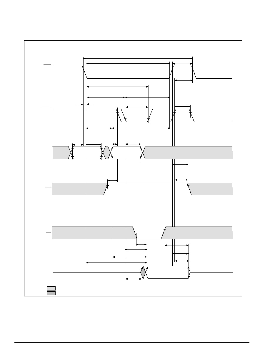
∑ Read Cycle
t
RC
t
RAS
t
RP
t
CRP
t
CPN
t
RRH
t
RCH
t
OEZ
t
OFF
t
OEA
t
CAC
t
AA
t
RAC
tCLZ
D
OUT
t
RCS
t
ASR
t
RAH
t
ASC
t
CAH
t
RAD
t
RAL
t
CAS
t
RSH
t
RCD
t
T
t
CSH
RAS
CAS
ADDRESS
WE
DQ1~DQ4
Note : = don't care
OE
t
OFF
Row
Column
= Invalid Dout
Rev.1
Page 16
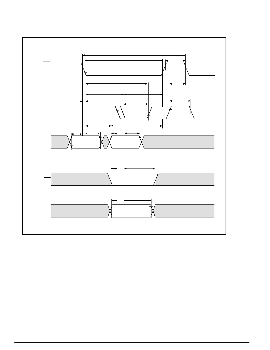
∑Early Write Cycle
t
RC
t
RAS
t
RP
t WCH
t
DS
t
DH
tWCS
t
RAL
t
CAS
t
RSH
t
RCD
t
T
t
CSH
RAS
CAS
WE
DQ1~DQ4
t
CRP
t
ASR
t
RAH
t
ASC
t
CAH
ADDRESS
Column
Row
t
CPN
DIN
t
RAD
t
RAL
Rev.1
Page 17
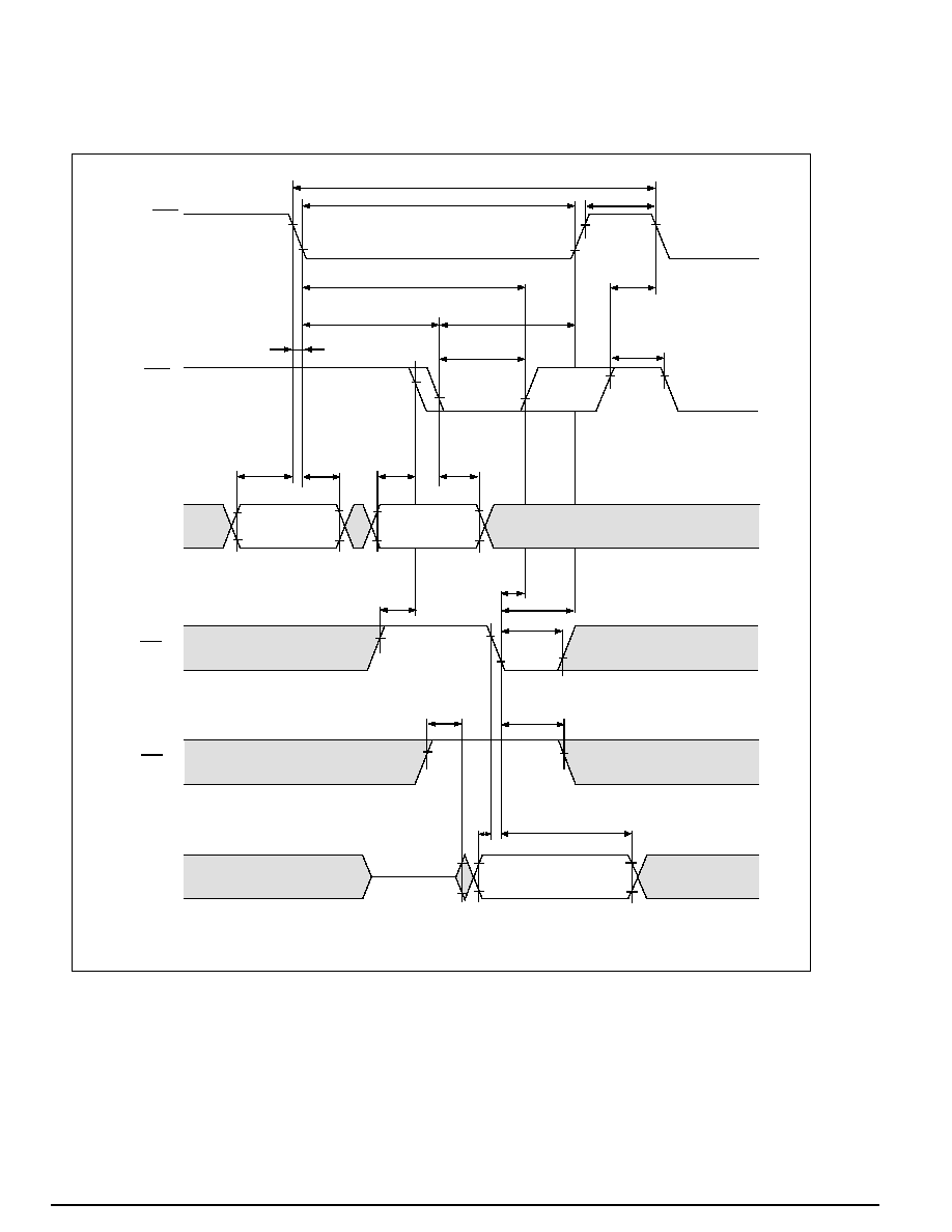
∑ Delayed Write Cycle
t
RC
t
RAS
t
RP
t RWL
t RCS
t
CAS
t
RSH
t
RCD
t
T
t
CSH
RAS
CAS
t
ASR
t
RAH
t
CAH
ADDRESS
Column
Row
t
ASC
D
IN
DQ1~DQ4
WE
t
CRP
t
CPN
t
DH
t
DS
t OEH
t OED
OE
t
DS
OPEN
t WP
tCWL

Rev.1
Page 18
∑ Read - Modify - Write Cycle
t
RWC
t
RAS
tRP
t
RWD
t
WP
t
RAD
t
RWL
t
CAS
t
CWL
t
RCD
t
T
t
CPN
RAS
CAS
WE
t
CRP
t
ASR
t
RAH
t
ASC
t
CAH
ADDRESS
Column
Row
DQ1~DQ4
t
DH
tDS
OE
t
RCS
t
AWD
t
CWD
D
IN
tOED
tOEH
tOEZ
tOEA
tCAC
tRAC
tAA
DQ1~DQ4
D
OUT
OPEN
t
DZC
t
DZO
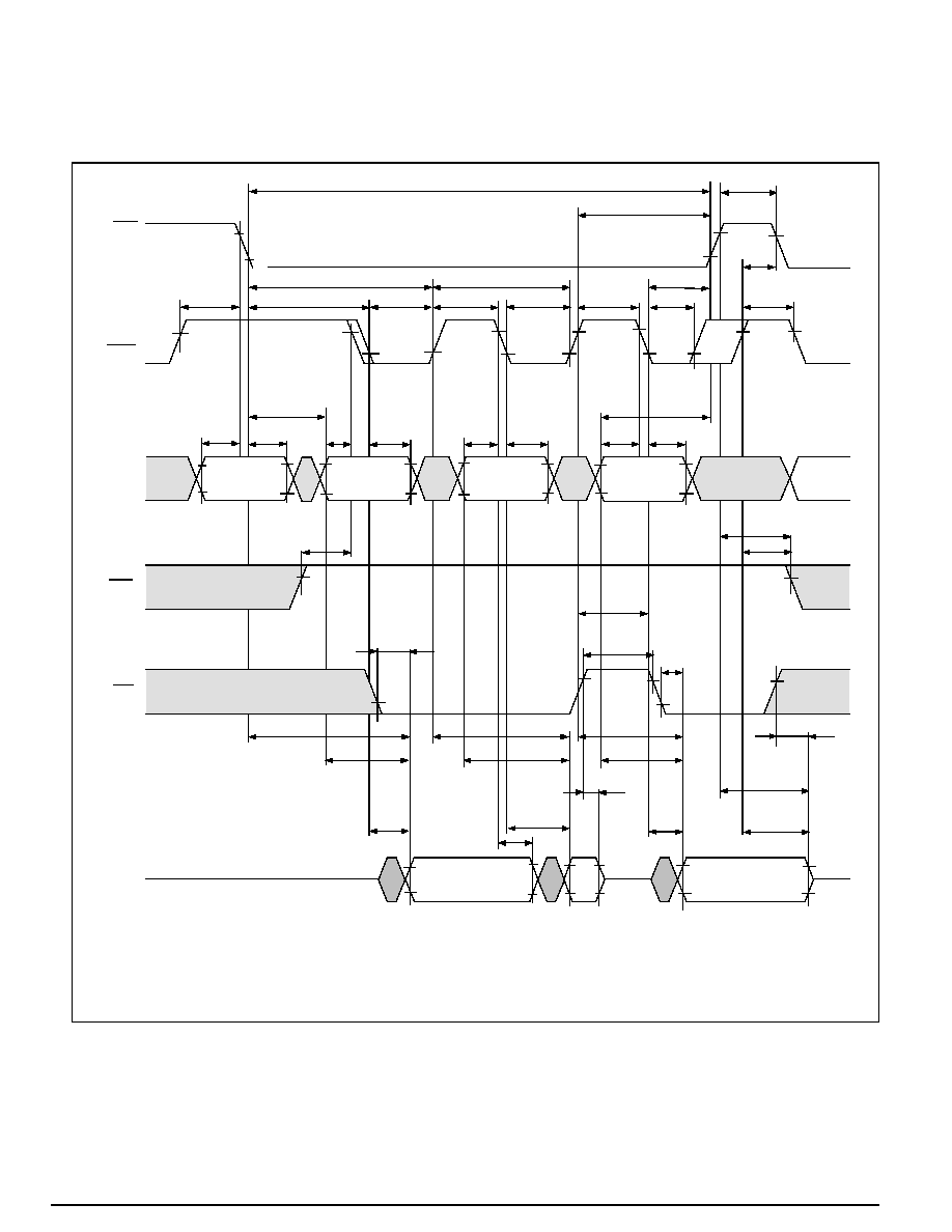
Rev.1
Page 19
∑ EDO Page Mode Read Cycle
t
RASP
t
CPRH
tRCS
t
CAS
t
RSH
t
RCD
tOEA
t
CSH
RAS
CAS
t
ASR
t
RAH
t
CAH
ADDRESS
t
CAS
WE
t
CRP
t CP
OE
DQ1~DQ4
OPEN
t
OEP
D
OUT
1
t
PC
t
CP
t
CAS
t
CPN
t
CRP
t
RAD
t
CAH
t
ASC
t
ASC
t
CAH
t
ASC
t
RAL
Row
Column 1
tOEA
tOEHC
t
RRH
t
RCH
tRAC
tAA
tAA
tAA
tCPA
tCPA
tOEZ
tOFF
tOFF
tCAC
tOEZ
tCAC
tCAC
tCOH
D
OUT
N
WE
OE
Column 2
Column N
Row
t
RP
D
OUT
2

Rev.1
Page 20
∑ EDO Page Mode Early Write Cycle
t
RASP
t
RP
tWCS
t
CAS
t
RSH
t
RCD
RAS
CAS
t
ASR
t
RAH
t
CAH
ADDRESS
t
CAS
WE
t CP
DQ1~DQ4
t
PC
t
CP
t
CAS
t
CPN
t
CRP
t
CAH
t
ASC
t
ASC
t
CAH
t
ASC
Row
Column 1
tDS
WE
Column 2
Column N
tWCH
tWCS
tWCH
tWCS
tWCH
tDH
tDS
tDH
tDS
tDH
D
IN
1
D
IN
2
D
IN
N
tT
t
CSH
Rev.1
Page 21
∑ EDO Page Mode Read-Early-Write Cycle
t
RASP
t
CPRH
tRCS
t
CAS
t
RSH
t
RCD
tOEA
t
CSH
RAS
CAS
t
ASR
t
RAH
t
CAH
ADDRESS
t
CAS
WE
t
CRP
t CP
OE
DQ1~DQ4
OPEN
t
WED
t
PC
t
CP
t
CAS
t
CPN
t
CRP
t
RAD
t
RAH
t
ASC
t
ASC
t
CAH
t
ASC
t
RAL
Row
Column 1
t
WCS
t
RCH
tRAC
tAA
tAA
tCPA
tDH
tWHZ
tCAC
tCAC
tCOH
WE
OE
Column 2
Column N
Row
t
RP
t
CAL
t
WCH
Data
Doutput 2
Data
Input N
Data
Doutput 1
tDS
t
CSH

Rev.1
Page 22
∑ EDO Page Mode Read-Modify-Write Cycle
tRASP
tCPRH
tRCS
t
CAS
tWP
RAS
CAS
t
ASR
t
RAH
t
CAH
ADDRESS
t
CAS
WE
t
RCD
CP
DQ1~DQ4
t
PRWC
t
CP
t
CAS
t
CRP
t
RAD
t
CAH
t
ASC
t
ASC
t
CAH
t
ASC
Row
Column 1
t
RWL
t
RCS
tOED
tDZO
tCAC
WE
OE
tRP
t
RAL
DOUT
2
DOUT
N
D
OUT
1
t
T
t
Column N
Column 2
Column 1
t
RWD
t
AWD
t
CWD
t
CWL
t
RCS
t
CWD
t
AWD
t
CPW
t
CWL
t
CPW
t
AWD
t
CWD
t
CWL
tOED
tOED
tOEH
tOEH
tOEH
tCAC
tCAC
tOEA
tAA
tRAC
tOEZ
tOEA
tAA
tCPA
tOEZ
tOEA
tAA
tCPA
tOEZ
tDS
tDH
tWP
tDS
tDH
tWP
tDS
tDH
OPEN
OPEN
OPEN
D
IN
1
D
IN
N
D
IN
2
DQ1~DQ4
tDZC
tDZO
tDZC
tDZC
tDZO

Rev.1
Page 23
∑ Read Cycle with WE Controlled Disable
t WPZ
t RCS
t
CAS
t
RCD
t
T
t
CSH
RAS
CAS
t
ASR
t
RAH
t
CAH
ADDRESS
Column
Row
t
ASC
D
DQ1~DQ4
WE
tOEZ
t
DS
tWHZ
OE
t RCH
tOEA
tCAC
tAA
tRAC
tCLZ
OUT
t
RAD

Rev.1
Page 24
RAS-Only Refresh Cycle
RAS
ADDRESS
tRC
tCRP
tASR
tRAH
tT
tRPC
ROW
tOFF
CAS
tRAS
tRP
OPEN
tCRP
DQ1~DQ4
RAS
tCSR
tWSR
tRP
tT
tRPC
tOFF
CAS
tRAS
tRP
OPEN
tCRP
DQ1~DQ4
tRPC
tCHR
tRAS
tRP
tRC
tRC
tCHR
tCSR
tWHR
tWSR
tWHR
WE
CAS-Before-RAS Refresh Cycle
Rev.1
Page 25
CBR Self-Refesh Cycle
RAS
WE
tRPC
tOFF
tCSR
tCHS
tWSR
CAS
tRASS
tRPS
OPEN
DQ1~DQ4
tWHR
High lmpedance

Rev.1
Page 26
∑ Hidden Refresh Cycle
tRP
tRAS
RAS
tRCD
tCRP
ADDRESS
WE
tCHR
tCAS
tRSH
t RAH
tASR
tASC
tCAH
tRAL
ROW
tRCH
tOEZ
CAS
DQ1~DQ4
tT
t RCS
D
tRAS
tRAS
tRP
tRP
tRC
tRC
tRC
t RAD
tRRH
tOFF
t OFF
t OEA
tCAC
tAA
t RAC
COlumn
OUT
OE
(READ)
(REFRESH)
(REFRESH)
Rev.1
Page 27
Ordering information
AD404M42VSA-5
∑ AD
∑ Ascend Memory Product
∑
40
∑ Device Type
∑ 4M4
∑ Density and Organization
∑ 2
∑ Refresh Rate, 2: 2K Refresh
∑ V
∑ T: 5V, V: 3.3V
∑ S
∑ Package Type (S : SOJ, T : TSOP II)
∑ A
∑ Version
∑ 5
∑ Speed (5: 50 ns, 6: 60 ns)
Part Number
Access time
Package
AD404M42VSA-5
AD404M42VSA-6
AD404M42VTA-5
AD404M42VTA-6
50 ns
60 ns
50 ns
60 ns
300mil 26/24-Pin
Plastic SOJ
TSOP II
Packaging information
∑
300 mil, 26/24-Pin Plastic SOJ
SEATING PLANE
4-e
e
b
b2
0.007"M
C
L
0.025" MIN.
0.004"
SECTION B-B
E2
A
RAD R1
A1
B
B
D
26
21
E
E1
19
14
BASE METAL
WITH PLATING
c1 c
b1
b
0.267 BASIC
0.335 BASIC
0.050 BASIC
R1
e
E1
E2
6.78 BASIC
1.27 BASIC
0.76
---
7.49
7.62
1.02
0.030
7.75
0.295
17.02
b
D
E
c1
b2
c
b1
A1
A
DIM
0.51
0.41
0.016
8.51 BASIC
0.18
17.15
---
0.66
0.18
0.41
---
---
0.46
17.27
0.28
0.670
0.007
0.81
0.30
0.48
0.007
0.026
0.016
MILLIMETERS
MIN.
NOM.
2.08
3.25
---
---
3.51
MAX.
MIN.
---
3.76
0.082
0.128
0.305
0.040
---
0.300
0.020
0.032
0.019
0.012
0.680
0.011
0.675
---
0.018
---
---
MAX.
0.148
---
NOM.
---
0.138
---
INCHES
2. DIMENSION D DOES NOT INCLUDE MOLD PROTRUSION.
DIMENSION E1 DOES NOT INCLUDE INTERLEAD PROTRUSION.
MOLD PROTRUSION SHALL NOT EXCEED 0.006"(0.15mm) PER SIDE.
INTERLEAD PROTRUSION SHALL NOT EXCEED 0.01"(0.25mm) PER SIDE.
1. CONTROLLING DIMENSION : INCHES
NOTE:
3. DIMENSION b2 DOES NOT INCLUDE DAMBAR PROTRUSION OR
TO LESS THAN 0.001"(0.025mm) BELOW b2 MIN.
DAMBAR INTRUSION SHALL NOT REDUCE THE SHOULDER WIDTH
SHOULDER WIDTH TO EXCEED b2 MAX BY MORE THAN 0.005"(0.127mm)
INTRUSION. DAMBAR PROTRUSION SHALL NOT CAUSE THE
1
6
8
13
A2
A2
2.54 REF.
0.100 REF.

Rev.1
Page 28
∑
300 mil, 26/24-Pin TSOP II
D
(ZD)
b
M
REF.
4-1.27
6
8
1
26
19
21
RAD R1
A2
E
E1
SEATING PLANE
0.100(0.004")
e
A
RAD R
A1
L
DETAIL A
13
DETAIL A
0 ~5
B
c
B
14
b
SECTION B-B
BASE METAL
WITH PLATING
b1
c
c1
0.024
0.020
0.60
0.016
0.40
0.50
L
0.12
0.12
R
R1
---
---
---
0.25
0.005
0.005
---
0.010
---
---
0.0374 BASIC
0.050 BASIC
0.16
0.005
c1
0.12
0.15
17.01
9.02
7.49
e
E1
E
D
ZD
1.27 BASIC
7.62
9.22
7.75
9.42
0.355
0.295
17.27
17.14
0.95 REF.
0.670
0.95
0.05
0.12
0.30
0.30
c
b1
A2
A1
b
---
0.40
0.21
0.45
0.005
0.012
1.00
---
---
1.05
0.15
0.037
0.002
0.012
0.52
(0.006)
0.006
0.305
0.371
0.300
0.363
0.680
0.675
0.008
0.018
---
0.016
0.041
0.006
0.020
0.039
---
---
---
A
DIM
MIN.
---
NOM.
MILLIMETERS
1.20
MAX.
---
MIN.
0.047
MAX.
---
INCHES
NOM.
0.200(0.008")
ALLOWABLE DAMBAR PROTRUSION SHALL NOT CAUSE THE LEAD TO
3. DIMENSION b DOES NOT INCLUDE DAMBAR PROTRUSIONS/INTRUSION.
INTERLEAD PROTRUSION SHALL NOT EXCEED 0.25(0.01") PER SIDE.
MOLD PROTRUSION SHALL NOT EXCEED 0.15(0.006") PER SIDE.
2. DIMENSION D DOES NOT INCLUDE MOLD PROTRUSION.
1. CONTROLLING DIMENSION : MILLIMETERS
NOTE:
THAN THE MIN b DIMENSION BY MORE THAN 0.07mm.
DAMBAR INTRUSION SHALL NOT CAUSE THE LEAD TO BE NARROWER
BE WIDER THAN THE MAX b DIMENSION BY MORE THAN 0.13mm.
DIMENSION E1 DOES NOT INCLUDE INTERLEAD PROTRUSION.