 | –≠–ª–µ–∫—Ç—Ä–æ–Ω–Ω—ã–π –∫–æ–º–ø–æ–Ω–µ–Ω—Ç: BBA-322-A | –°–∫–∞—á–∞—Ç—å:  PDF PDF  ZIP ZIP |
GENERAL-PURPOSE BROADBAND RF AMPLIFIER DATA GUIDE
s
TX/RX Range Enhancement*
s
IF or RF Buffering
s
Driver or Final Stage for PA
s
General-Purpose Gain Blocks
APPLICATIONS INCLUDE:
s
Prematched for 50
Impedance I/O
s
No External RF Components Required
s
Exceptional Gain Flatness
s
Compact Surface-Mount Package
(for easy hand or automated mounting)
s
High Gain Model
s
10 Mhz-3 Ghz Broadband Operation
s
+20dB Small Signal Gain @ 900MHz
s
Up to +10 (10mW) Linear Output Power
s
3.8 dB Noise Figure
s
Operates From a Single Supply
BBA-322 FEATURES:
BBA- 519 FEATURES:
s
High Output Model
s
10 Mhz-4 Ghz Broadband Operation
s
+18dB Small Signal Gain @ 900MHz
s
Up to +17 (50mW) Linear Output Power
s
4.8 dB Noise Figure
s
Operates From a Single Supply
The BBA series is a family of low-cost
high-performance broadband RF
amplifiers.
The modules are ideally
suited to a wide range of amplification
and buffering applications including
extending the range of Linx's own RF
modules (when legally appropriate).
Housed in a compact SMD package, the
hybrid amps are prematched to 50
source and load impedances and require
no external RF components.
The
modules utilize a GaHBT gain stage
which yields high gain and IP3, excellent
flatness and low noise.
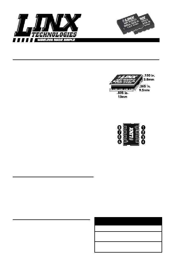
BBA-322-A
BBA-519-A
RF OUT
GND
GND
GND
RF IN
GND
GND
VCC
PINOUTS (BOTTOM VIEW)
PHYSICAL DIMENSIONS
DESCRIPTION:
ALL BBA AMPS FEATURE:
Revised 1/26/01
PART # DESCRIPTION
BBA-322-A
Hi-Gain RF Amp
BBA-519-A
Hi-Power RF Amp
BBA Amplifiers are supplied in tube
packaging - 50 pcs. per tube.
ORDERING INFORMATION
Page 2
PERFORMANCE DATA ≠ BBA-519-A
ABSOLUTE MAXIMUM RATINGS
These ratings are intended to indicate the limits
past which device damage may occur.
Operation of the device at these limits is not
suggested or guaranteed.
TYPICAL OPERATING PARAMETERS
All parameters measured @ 5.2 Volts, 25∞C, -30dBm input
Page 2
Parameters
BBA-519-A
Typical
Units
Notes
Frequency Range
10 to 4000
MHz
T=25∞C, I
cc
=65mA
Gain
18
dB
Freq=100MHz
17
dB
Freq=1000MHz
15
dB
Freq=2000MHz
13
dB
Freq=3000MHz
12
dB
Freq=4000MHz
Gain Flatness
±2
dB
100MHz to 2000MHz
Noise Figure
4.8
dB
Freq=2000MHz
Input VSWR
2.1:1
In a 50
system, DC to 4000MHz
Output VSWR
1.8:1
In a 50
system, DC to 4000MHz
Output IP
3
+33
dBm
Freq=1000MHz±50KHz, P
TONE
=-10dBm
Output P
1dB
+18.5
dBm
Freq=1000MHz
Reverse Isolation
20
dB
Freq=2000MHz
Power Supply
Device Operating Voltage
4.8-5.2
VDC
VCC regulated between 4.8 and 5.2VDC
5.2-12
VDC
VCC Range using appropriate current limiting
resistor inline with VCC
Operating Current
60
mA
@5VDC
Environmental
Rated Operating
Temperature
0-70
∞C
Parameters BBA-519-A
Rating
Unit
Supply Current
120
mA
Input RF Power
+13
dBm
Environmental Operating Temp.
-40 to +85
∞C
Storage Temp.
-60 to 150
∞C
ESD Sensitive Device
HANDLING
CAUTION
Page 3
PERFORMANCE DATA ≠ BBA-322-A
Parameters
Rating
Unit
Supply Current
65
mA
Input RF Power
+15
dBm
Environmental Operating Temp.
-40 to +85
∞C
Storage Temp.
-60 to 150
∞C
ABSOLUTE MAXIMUM RATINGS
TYPICAL OPERATING PARAMETERS
All parameters measured @ 5 Volts, 25∞C, -50dBm input
These ratings are intended to indicate the limits
past which device damage may occur.
Operation of the device at these limits is not
suggested or guaranteed.
Parameters
BBA-322-A
Typical
Units
Notes
Frequency Range
DC to 3000
MHz
T=25∞C, I
cc
=35mA
Gain
21
dB
Freq=100MHz
20
dB
Freq=1000MHz
17
dB
Freq=2000MHz
14
dB
Freq=3000MHz
Gain Flatness
±2
dB
100MHz to 2000MHz
Noise Figure
3.8
dB
Freq=2000MHz
Input VSWR
2.3:1
In a 50
system, DC to 3000MHz
Output VSWR
2.1:1
In a 50
system, DC to 3000MHz
Output IP3
+22.5
dBm
Freq=2000MHz±50KHz, P
TONE
=-18dBm
Output P1dB
+11.2
dBm
Freq=2000MHz
Reverse Isolation
20
dB
Freq=2000MHz
Power Supply
Device Operating
Voltage
4.8-5.2
VDC
VCC regulated between 4.8 and 5.2VDC
5.2-12
VDC
VCC Range using appropriate current limiting
resistor inline with VCC
Operating Current
35
mA
@ 5VDC
Environmental
Rated Operating
Temperature
0-70
∞C
ESD Sensitive Device
HANDLING
CAUTION
Page 4
OPERATIONAL CONSIDERATIONS
The use of a gain stage can produce a significant increase in the range
performance of an RF link. It is important to note that it can also introduce
detrimental effects such as the following:
∑ Amplification of harmonics and LO along with the fundamental carrier
frequency.
∑ Adverse effect on front-end noise figure on RX's.
∑ Potential damage if receiver input is not capable of accommodating high input
power levels.
∑ Risk of generating illegal power levels and unacceptable interference.
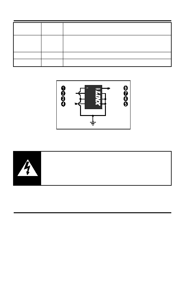
PIN DESCRIPTIONS:
RF IN
RF OUT
GND
GND
GND
GND
GND
VCC
Pin 1,3,5,6,7 GROUND
Pin 2
VCC
Pin 4
RF IN
Pin 8
RF OUT
Ground Connection. Keep traces short and connect
immediately to ground plane for best results.
VCC Positive Supply Voltage. Read the Power Supply
Considerations section of this manual carefully to
avoid permanent device damage
RF input pin. This pin is internally DC blocked.
RF output. This pin is internally DC blocked.
*IMPORTANT NOTE:
The purchaser of this device should be aware that approvals
may be required by applicable governing bodies for systems
producing RF energy. It is the responsibility of the user to
determine and adhere to the appropriate regulations for the
region in which operation is intended.
Page 5
POWER SUPPLY CONSIDERATIONS
The user should insure a clean source of power for the amplifier module. In
cases where the supply contains excessive noise, a filter and bypass should be
placed on the supply line in close proximity to the module.
The power supply must be regulated to within the primary range specified or the
maximum current limited using an appropriate resistance in series with the
amplifier's positive supply pin. Failure to observe the supply limits will irreparibly
damage the device. The resistor should be selected so that the device current is
limited to or less than the maximum rated current. The resistor value may be
easily selected using the following formula:
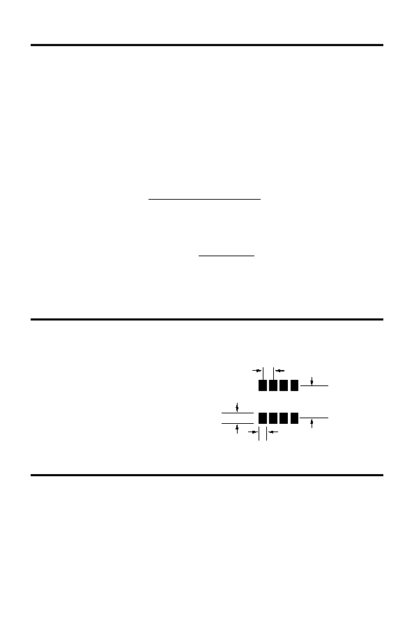
PAD LAYOUT
The pad layout shown below is designed to facilitate both hand and automated
assembly.
BOARD LAYOUT
If you are at all familiar with RF devices you may be concerned about specialized
layout requirements. Hi-gain high-frequency amplifiers are notorious for layout
challenges. Thankfully, the BBA series is inherently very stable. By adhering to a
few simple design and layout rules you will enjoy a trouble-free implementation.
The module should be placed as close as possible to the transmitter or receiver
with which it is to be paired. A ground plane should be placed under the module,
usually on the backside of the PCB. RF traces to and from the amp should be
kept short and of the proper width to assure service as a 50
transmission line.
The module's RF ports are AC-coupled and require no matching in a 50
system.
R=
V
SUPPLY
- V
DEVICE TYP.
I
CC
R=
9-5
60x10
-3
=
=
4˜.06
66
BBA Pad Layout Pattern
(Not to Scale)
0.100"
0.310"
0.100"
0.070"
Example:
BBA-519 @ 9 Volt Supply