Äîêóìåíòàöèÿ è îïèñàíèÿ www.docs.chipfind.ru
BC41B143A-db-001Pe
This material is subject to CSR's non-disclosure agreement
Production Information
© Cambridge Silicon Radio Limited 2005
Page 1 of 102
Device Features
_äìÉ`çêÉ
»
QJolj
Single Chip Bluetooth
®
v2.0 System
with EDR
Production Data Sheet for
BC41B143A
!
Fully Qualified Bluetooth v2.0 system
!
Enhanced Data Rate (EDR) compliant with
v2.0.E.2 of specification for both 2Mbps and
3Mbps modulation modes
!
Full Speed Bluetooth Operation with Full
Piconet Support
!
Scatternet Support
!
1.8V core, 1.7 to 3.6V I/O split rails
!
Low Power 1.8V Operation
!
Small footprint 6 x 6mm 84-ball VFBGA
Package
!
Minimal External Components Required
!
Integrated 1.8V regulator
!
USB and Dual UART Ports to 3MBaud
!
Support for 802.11 Coexistence
!
RoHS Compliant
July 2005
General Description
Applications
_äìÉ`çêÉQJolj is a single chip radio and
baseband IC for Bluetooth 2.4GHz systems
including enhanced data rates (EDR) to 3Mbps.
With the on-chip CSR Bluetooth software stack it
provides a fully compliant Bluetooth system to v2.0
of the specification for data and voice
communications.
!
Cellular Handsets
!
Personal Digital Assistants
!
Digital cameras and other high volume consumer
products
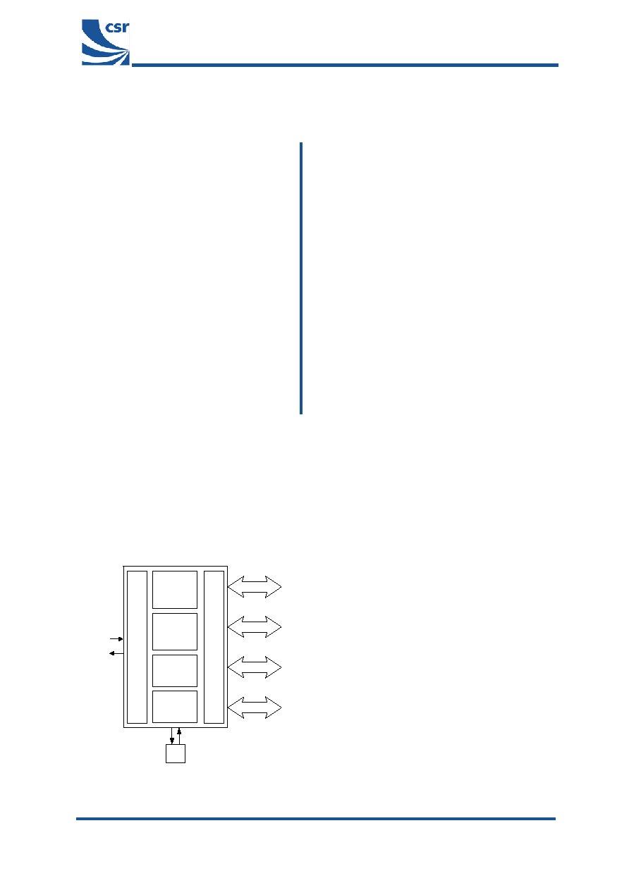
SPI
UART/USB
2.4
GHz
Radio
I/O
XTAL
RF OUT
RAM
Baseband
DSP
MCU
ROM
PIO
PCM
RF IN
BlueCore4-ROM System Architecture
BlueCore4-ROM has been designed to reduce the number
of external components required which ensures that
production costs are minimised.
The device incorporates auto-calibration and built-in
self-test (BIST) routines to simplify development, type
approval and production test. All hardware and device
firmware is fully compliant with the Bluetooth v2.0
Specification (all mandatory and optional features).
To improve the performance of both Bluetooth and
802.11b/g co-located systems a wide range of
co-existence features are available including a variety of
hardware signalling: basic activity signalling and Intel
WCS activity and channel signalling.

Status Information
BC41B143A-ds-001Pe
This material is subject to CSR's non-disclosure agreement
Production Information
© Cambridge Silicon Radio Limited 2005
Page 2 of 102
_äìÉ`çêÉ
»
QJolj
Product Data Sheet
Contents
Status Information ................................................................................................................................................ 7
1
Key Features .................................................................................................................................................. 8
2
6 x 6mm VFBGA Package Information ......................................................................................................... 9
2.1
BlueCore4-ROM Pinout Diagram ............................................................................................................ 9
2.2
Device Terminal Functions .................................................................................................................... 10
3
Electrical Characteristics ............................................................................................................................ 13
3.1
Power Consumption .............................................................................................................................. 18
4
Radio Characteristics Basic Data Rate ................................................................................................... 19
4.1
Temperature +20°C ............................................................................................................................... 19
4.1.1
Transmitter................................................................................................................................. 19
4.1.2
Receiver..................................................................................................................................... 21
4.2
Temperature -40°C................................................................................................................................ 23
4.2.1
Transmitter................................................................................................................................. 23
4.2.2
Receiver..................................................................................................................................... 23
4.3
Temperature -25°C................................................................................................................................ 24
4.3.1
Transmitter................................................................................................................................. 24
4.3.2
Receiver..................................................................................................................................... 24
4.4
Temperature +85°C ............................................................................................................................... 25
4.4.1
Transmitter................................................................................................................................. 25
4.4.2
Receiver..................................................................................................................................... 25
4.5
Temperature +105°C ............................................................................................................................. 26
4.5.1
Transmitter................................................................................................................................. 26
4.5.2
Receiver..................................................................................................................................... 26
5
Radio Characteristics Enhanced Data Rate............................................................................................ 27
5.1
Temperature +20°C ............................................................................................................................... 27
5.1.1
Transmitter................................................................................................................................. 27
5.1.2
Receiver..................................................................................................................................... 28
5.2
Temperature -40°C................................................................................................................................ 29
5.2.1
Transmitter................................................................................................................................. 29
5.2.2
Receiver..................................................................................................................................... 30
5.3
Temperature -25°C................................................................................................................................ 31
5.3.1
Transmitter................................................................................................................................. 31
5.3.2
Receiver..................................................................................................................................... 32
5.4
Temperature +85°C ............................................................................................................................... 33
5.4.1
Transmitter................................................................................................................................. 33
5.4.2
Receiver..................................................................................................................................... 34
5.5
Temperature +105°C ............................................................................................................................. 35
5.5.1
Transmitter................................................................................................................................. 35
5.5.2
Receiver..................................................................................................................................... 36
6
Device Diagram ............................................................................................................................................ 37
7
Description of Functional Blocks ............................................................................................................... 38
7.1
RF Receiver........................................................................................................................................... 38
7.1.1
Low Noise Amplifier ................................................................................................................... 38
7.1.2
Analogue to Digital Converter .................................................................................................... 38
7.2
RF Transmitter....................................................................................................................................... 38
7.2.1
IQ Modulator .............................................................................................................................. 38
7.2.2
Power Amplifier .......................................................................................................................... 38
7.2.3
Auxiliary DAC ............................................................................................................................. 38
7.3
RF Synthesiser ...................................................................................................................................... 38
7.4
Power Control and Regulation............................................................................................................... 38
7.5
Clock Input and Generation ................................................................................................................... 39
7.6
Baseband and Logic.............................................................................................................................. 39

Status Information
BC41B143A-ds-001Pe
This material is subject to CSR's non-disclosure agreement
Production Information
© Cambridge Silicon Radio Limited 2005
Page 3 of 102
_äìÉ`çêÉ
»
QJolj
Product Data Sheet
7.6.1
Memory Management Unit......................................................................................................... 39
7.6.2
Burst Mode Controller ................................................................................................................ 39
7.6.3
Physical Layer Hardware Engine DSP....................................................................................... 39
7.6.4
RAM ........................................................................................................................................... 39
7.6.5
ROM........................................................................................................................................... 39
7.6.6
USB............................................................................................................................................ 40
7.6.7
Synchronous Serial Interface ..................................................................................................... 40
7.6.8
UART ......................................................................................................................................... 40
7.6.9
Audio PCM Interface .................................................................................................................. 40
7.7
Microcontroller ....................................................................................................................................... 40
7.7.1
Programmable I/O...................................................................................................................... 40
7.7.2
802.11 Coexistence Interface .................................................................................................... 40
8
CSR Bluetooth Software Stacks ................................................................................................................. 41
8.1
BlueCore HCI Stack .............................................................................................................................. 41
8.1.1
Key Features of the HCI Stack Standard Bluetooth Functionality ........................................... 42
8.1.2
Key Features of the HCI Stack Extra Functionality ................................................................. 43
8.2
BlueCore RFCOMM Stack..................................................................................................................... 44
8.2.1
Key Features of the BlueCore4-ROM RFCOMM Stack ............................................................. 45
8.3
BlueCore Virtual Machine Stack ............................................................................................................ 46
8.4
BCHS Software ..................................................................................................................................... 47
8.5
Additional Software for Other Embedded Applications .......................................................................... 47
8.6
CSR Development Systems .................................................................................................................. 47
9
Enhanced Data Rate .................................................................................................................................... 48
9.1
Enhanced Data Rate Baseband ............................................................................................................ 48
9.2
Enhanced Data Rate
/4 DQPSK.......................................................................................................... 48
9.3
Enhanced Data Rate 8DPSK................................................................................................................. 49
10
Device Terminal Descriptions..................................................................................................................... 51
10.1
RF Ports ................................................................................................................................................ 51
10.1.1
TX_A and TX_B ......................................................................................................................... 51
10.1.2
Single-Ended Input (RF_IN)....................................................................................................... 52
10.1.3
Transmit RF Power Control for Class 1 Applications (TX_PWR) ............................................... 52
10.1.4
Control of External RF Components .......................................................................................... 53
10.2
External Reference Clock Input (XTAL_IN) ........................................................................................... 54
10.2.1
External Mode ............................................................................................................................ 54
10.2.2
XTAL_IN Impedance in External Mode ...................................................................................... 54
10.2.3
Clock Timing Accuracy............................................................................................................... 54
10.2.4
Clock Start-Up Delay.................................................................................................................. 55
10.2.5
Input Frequencies and PS Key Settings..................................................................................... 56
10.3
Crystal Oscillator (XTAL_IN, XTAL_OUT) ............................................................................................. 57
10.3.1
XTAL Mode ................................................................................................................................ 57
10.3.2
Load Capacitance ...................................................................................................................... 58
10.3.3
Frequency Trim .......................................................................................................................... 58
10.3.4
Transconductance Driver Model ................................................................................................ 59
10.3.5
Negative Resistance Model ....................................................................................................... 59
10.3.6
Crystal PS Key Settings ............................................................................................................. 59
10.3.7
Crystal Oscillator Characteristics ............................................................................................... 60
10.4
UART Interface...................................................................................................................................... 63
10.4.1
UART Bypass............................................................................................................................. 65
10.4.2
UART Configuration While RESET is Active.............................................................................. 65
10.4.3
UART Bypass Mode................................................................................................................... 65
10.4.4
Current Consumption in UART Bypass Mode............................................................................ 65
10.5
USB Interface ........................................................................................................................................ 66
10.5.1
USB Data Connections .............................................................................................................. 66
10.5.2
USB Pull-Up Resistor................................................................................................................. 66
10.5.3
Power Supply ............................................................................................................................. 66
10.5.4
Self Powered Mode.................................................................................................................... 67
10.5.5
Bus Powered Mode.................................................................................................................... 68
10.5.6
Suspend Current ........................................................................................................................ 69

Status Information
BC41B143A-ds-001Pe
This material is subject to CSR's non-disclosure agreement
Production Information
© Cambridge Silicon Radio Limited 2005
Page 4 of 102
_äìÉ`çêÉ
»
QJolj
Product Data Sheet
10.5.7
Detach and Wake-Up Signalling ................................................................................................ 69
10.5.8
USB Driver ................................................................................................................................. 69
10.5.9
USB 1.1 Compliance.................................................................................................................. 70
10.5.10
USB 2.0 Compatibility........................................................................................................... 70
10.6
Serial Peripheral Interface ..................................................................................................................... 70
10.6.1
Instruction Cycle......................................................................................................................... 70
10.6.2
Writing to BlueCore4-ROM ........................................................................................................ 71
10.6.3
Reading from BlueCore4-ROM .................................................................................................. 71
10.6.4
Multi Slave Operation................................................................................................................. 71
10.7
Audio PCM Interface ............................................................................................................................. 72
10.7.1
PCM Interface Master/Slave ...................................................................................................... 73
10.7.2
Long Frame Sync....................................................................................................................... 74
10.7.3
Short Frame Sync ...................................................................................................................... 74
10.7.4
Multi Slot Operation.................................................................................................................... 75
10.7.5
GCI Interface.............................................................................................................................. 75
10.7.6
Slots and Sample Formats......................................................................................................... 76
10.7.7
Additional Features .................................................................................................................... 76
10.7.8
PCM Timing Information ............................................................................................................ 77
10.7.9
PCM Slave Timing ..................................................................................................................... 79
10.7.10
PCM_CLK and PCM_SYNC Generation.................................................................................. 81
10.7.11
PCM Configuration ................................................................................................................... 82
10.8
I/O Parallel Ports ................................................................................................................................... 83
10.8.1
PIO Defaults for BTv2.0 + EDR HCI Level Bluetooth Stack ....................................................... 83
10.9
I
2
C Interface........................................................................................................................................... 84
10.10
TCXO Enable OR Function.................................................................................................................. 84
10.11
RESET and RESETB........................................................................................................................... 85
10.11.1
Pin States on Reset ................................................................................................................. 86
10.11.2
Status after Reset .................................................................................................................... 86
10.12
Power Supplies .................................................................................................................................... 87
10.12.1
Supply Domains and Sequencing ............................................................................................ 87
10.12.2
External Voltage Source........................................................................................................... 87
10.12.3
Linear Regulator....................................................................................................................... 87
10.12.4
VREG_EN Pin.......................................................................................................................... 87
11
Application Schematic................................................................................................................................. 88
12
Package Dimensions ................................................................................................................................... 89
12.1
6 x 6mm VFBGA 84-Ball Package......................................................................................................... 89
13
Solder Profiles.............................................................................................................................................. 90
13.1
Solder Re-Flow Profile for Devices with Lead-Free Solder Balls ........................................................... 90
14
Ordering Information ................................................................................................................................... 92
14.1
BlueCore4-ROM .................................................................................................................................... 92
15
Tape and Reel Information .......................................................................................................................... 93
15.1
Tape Orientation and Dimensions ......................................................................................................... 93
15.2
Reel Information .................................................................................................................................... 95
15.3
Dry Pack Information ............................................................................................................................. 96
15.4
Baking Conditions.................................................................................................................................. 97
15.5
Product Information ............................................................................................................................... 97
16
Contact Information ..................................................................................................................................... 98
17
Document References ................................................................................................................................. 99
Terms and Definitions ...................................................................................................................................... 100
Document History ............................................................................................................................................. 102

Status Information
BC41B143A-ds-001Pe
This material is subject to CSR's non-disclosure agreement
Production Information
© Cambridge Silicon Radio Limited 2005
Page 5 of 102
_äìÉ`çêÉ
»
QJolj
Product Data Sheet
List of Figures
Figure 2.1: BlueCore4-ROM Device Pinout ............................................................................................................ 9
Figure 6.1: BlueCore4-ROM Device Diagram ....................................................................................................... 37
Figure 8.1: BlueCore HCI Stack ............................................................................................................................ 41
Figure 8.2: BlueCore RFCOMM Stack .................................................................................................................. 44
Figure 8.3: Virtual Machine ................................................................................................................................... 46
Figure 9.1: Basic Data Rate and Enhanced Data Rate Packet Structure.............................................................. 48
Figure 9.2:
/4 DQPSK Constellation Pattern ....................................................................................................... 49
Figure 9.3: 8DPSK Constellation Pattern .............................................................................................................. 50
Figure 10.1: Circuit TX/RX_A and TX/RX_B ......................................................................................................... 51
Figure 10.2: Circuit RF_IN .................................................................................................................................... 52
Figure 10.3: Internal Power Ramping.................................................................................................................... 53
Figure 10.4: TCXO Clock Accuracy ...................................................................................................................... 54
Figure 10.5: Actual Allowable Clock Presence Delay on XTAL_IN vs. PS Key Setting......................................... 55
Figure 10.6: Crystal Driver Circuit ......................................................................................................................... 57
Figure 10.7: Crystal Equivalent Circuit .................................................................................................................. 57
Figure 10.8: Crystal Load Capacitance and Series Resistance Limits with Crystal Frequency............................. 60
Figure 10.9: Crystal Driver Transconductance vs. Driver Level Register Setting.................................................. 61
Figure 10.10: Crystal Driver Negative Resistance as a Function of Drive Level Setting ....................................... 62
Figure 10.11: Universal Asynchronous Receiver .................................................................................................. 63
Figure 10.12: Break Signal.................................................................................................................................... 64
Figure 10.13: UART Bypass Architecture ............................................................................................................. 65
Figure 10.14: USB Connections for Self Powered Mode ...................................................................................... 67
Figure 10.15: USB Connections for Bus Powered Mode ...................................................................................... 68
Figure 10.16: USB_DETACH and USB_WAKE_UP Signal .................................................................................. 69
Figure 10.17: Write Operation............................................................................................................................... 71
Figure 10.18: Read Operation............................................................................................................................... 71
Figure 10.19: BlueCore4-ROM as PCM Interface Master ..................................................................................... 73
Figure 10.20: BlueCore4-ROM as PCM Interface Slave ....................................................................................... 73
Figure 10.21: Long Frame Sync (Shown with 8-bit Companded Sample)............................................................. 74
Figure 10.22: Short Frame Sync (Shown with 16-bit Sample) .............................................................................. 74
Figure 10.23: Multi Slot Operation with Two Slots and 8-bit Companded Samples .............................................. 75
Figure 10.24: GCI Interface................................................................................................................................... 75
Figure 10.25: 16-Bit Slot Length and Sample Formats ......................................................................................... 76
Figure 10.26: PCM Master Timing Long Frame Sync ........................................................................................... 78
Figure 10.27: PCM Master Timing Short Frame Sync........................................................................................... 78
Figure 10.28: PCM Slave Timing Long Frame Sync ............................................................................................. 80
Figure 10.29: PCM Slave Timing Short Frame Sync............................................................................................. 80
Figure 10.30: Example EEPROM Connection ...................................................................................................... 84
Figure 10.31: Example TXCO Enable OR Function .............................................................................................. 84
Figure 13.1: Application Circuit for Radio Characteristics Specification with 6 x 6mm VFBGA Package .............. 88
Figure 14.1: BlueCore4-ROM 84-Ball VFBGA Package Dimensions.................................................................... 89
Figure 15.1: Typical Lead-Free Re-flow Solder Profile.......................................................................................... 90
Figure 17.1: Tape and Reel Orientation ................................................................................................................ 93
Figure 17.2: Tape Dimensions .............................................................................................................................. 94
Document Outline
- þÿ
- þÿ
- þÿ
- þÿ
- þÿ
- þÿ
- þÿ
- þÿ
- þÿ
- þÿ
- þÿ
- þÿ
- þÿ
- þÿ
- þÿ
- þÿ
- þÿ
- þÿ
- þÿ
- þÿ
- þÿ
- þÿ
- þÿ
- þÿ
- þÿ
- þÿ
- þÿ
- þÿ
- þÿ
- þÿ
- þÿ
- þÿ
- þÿ
- þÿ
- þÿ
- þÿ
- þÿ
- þÿ
- þÿ
- þÿ
- þÿ
- þÿ
- þÿ
- þÿ
- þÿ
- þÿ
- þÿ
- þÿ
- þÿ
- þÿ
- þÿ
- þÿ
- þÿ
- þÿ
- þÿ
- þÿ
- þÿ
- þÿ
- þÿ
- þÿ
- þÿ
- þÿ
- þÿ
- þÿ
- þÿ
- þÿ
- þÿ
- þÿ
- þÿ
- þÿ
- þÿ