C-51496GNFJ-AB (AB) No. 2002-0119
OPTREX CORPORATION
Page 1/16
LCD Module Technical Specification
C-51496GNFJ-AB
Table of Contents
1. General Specifications
.................................................................................................................................. 2
2. Electrical Specifications
............................................................................................................................... 3
3. Optical Specifications
................................................................................................................................... 6
4. I/O Terminal
...................................................................................................................................................... 8
5. Test
................................................................................................................................................................... 10
6. Appearance Standards
............................................................................................................................... 11
7. Code System of Production Lot
............................................................................................................... 14
8. Type Number
.................................................................................................................................................. 14
9. Applying Precautions
.................................................................................................................................. 14
10. Precautions Relating Product Handling
................................................................................................ 15
11. Warranty
........................................................................................................................................................ 16
Checked by (Design Engineering Div.)
Checked by (Quality Assurance Div.)
Approved by (Production Div.)
Prepared by (Production Div.)
Revision History
Rev.
Date
Page
Comment
Type No.
Apr 15, 2002
O P T R E X
First Edition
Final Revision
******
C-51496GNFJ-AB (AB) No. 2002-0119
OPTREX CORPORATION
Page 2/16
1. General Specifications
Operating Temp.
: min. -10
�
C ~ max. 60
�
C
Storage Temp.
: min. -20
�
C ~ max. 70
�
C
Display Format
: 16 characters
�
2 lines
Display Fonts
: 5
�
8 dots ( 1 character )
Viewing Area
: 61.0 (W)
�
16.5 (H) mm
Outline Dimensions
: 64.0
*
(W)
�
25.0
**
(H)
�
2.2 max. (D) mm
*
Without Area of Injection Port
**
Without Flat Cable
Weight
: 7.4g max.
LCD Type
: NRD-21276
( F-STN / Black
&White-mode / Reflective )
Viewing Angle
: 6:00
Data Transfer
: 4-bit parallel data transfer
: Serial data transfer
Backlight
: None
Drawings
: Dimensional Outline UE-310928
C-51496GNFJ-AB (AB) No. 2002-0119
OPTREX CORPORATION
Page 4/16
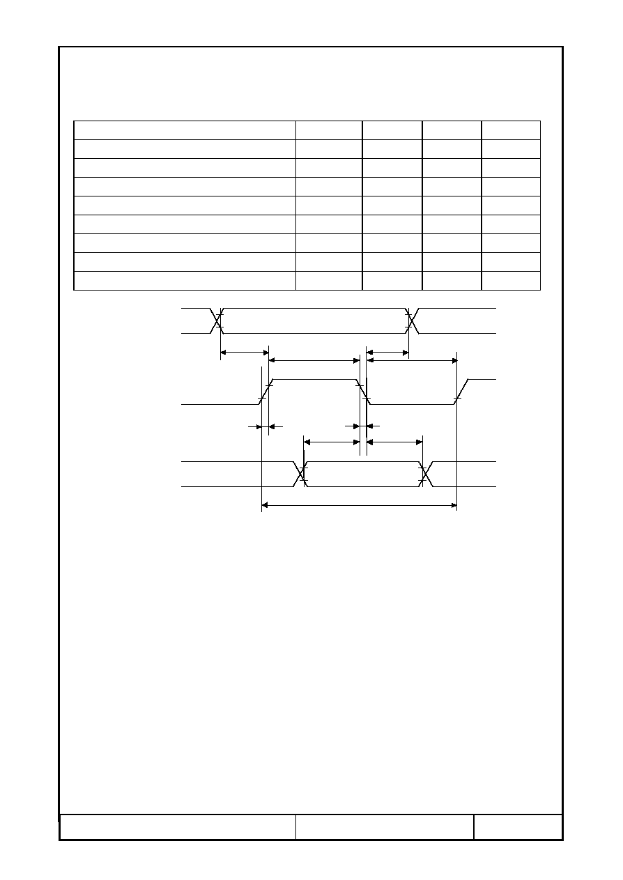
2.3. AC Characteristics
2.3.1. 4 Bit Bus Interface Timing
V
CC
=2.8~3.2V
Parameter
Symbol
Min.
Max.
Units
Enable Cycle Time
t
CYCE
500
-
ns
Enable High Level Pulse Width
PW
EH
80
-
ns
Enable Low Level Pulse Width
PW
EL
250
-
ns
Enable Rise/Fall Time
t
E
r,
t
E
f
-
25
ns
Setup Time (RS to E,CS*)
t
ASE
60
-
ns
Address Hold Time
t
AHE
20
-
ns
Write Data Setup Time
t
DSWE
60
-
ns
Write Data Hold Time
t
HE
20
-
ns
E/SCL
V
IH
t
CYC
t
E
r
t
E
f
t
DSW E
t
D H W E
t
AHE
t
ASE
V
IL
RS/CS*
DB0 /ID
DB1
DB3
Valid Data
V
IH
V
IL
V
IH
V
IL
V
IH
V
IL
V
IL
V
IH
V
IL
V
IH
V
IL
PW
EL
PW
EH
C-51496GNFJ-AB (AB) No. 2002-0119
OPTREX CORPORATION
Page 5/16
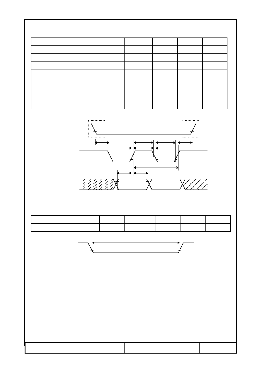
2.3.2. Serial Interface Sequence
V
CC
=2.8
3.2V
Parameter
Symbol
Min.
Max.
Units
Serial Clock Cycle Time
t
SCYC
0.2
20
�
s
Serial Clock High Level Width
t
SCH
80
-
ns
Serial Clock Low Level Width
t
SCL
80
-
ns
Serial Clock Rise/Fall Time
t
SC
r,
t
SC
f
-
20
ns
Chip Select Setup Time
t
CSU
60
-
ns
Chip Select Hold Time
t
CH
200
-
ns
Serial Input Data Setup Time
t
SISU
40
-
ns
Serial Input Data Hold Time
t
SIH
40
-
ns
2.3.3. Reset Timing
Parameter
Symbol
Conditions
Min.
Max.
Units
Reset Low Level Width
t
RES
-
1
-
ms
E/SCL
RS/CS*
SDA
V
IL
Start: S
End: P
V
IL
V
IH
V
IH
V
IH
V
IL
V
IH
V
IL
V
IL
t
CSU
t
SISU
t
SIH
Valid Data
Valid Data
t
SCYC
t
SC
r
t
SC
f
t
SCH
t
CH
t
SCL
RESET*
V
IL
t
RES
V
IL