 | –≠–ª–µ–∫—Ç—Ä–æ–Ω–Ω—ã–π –∫–æ–º–ø–æ–Ω–µ–Ω—Ç: CD13002 | –°–∫–∞—á–∞—Ç—å:  PDF PDF  ZIP ZIP |
NPN SILICON PLANAR EPITAXIAL, HIGH VOLTAGE
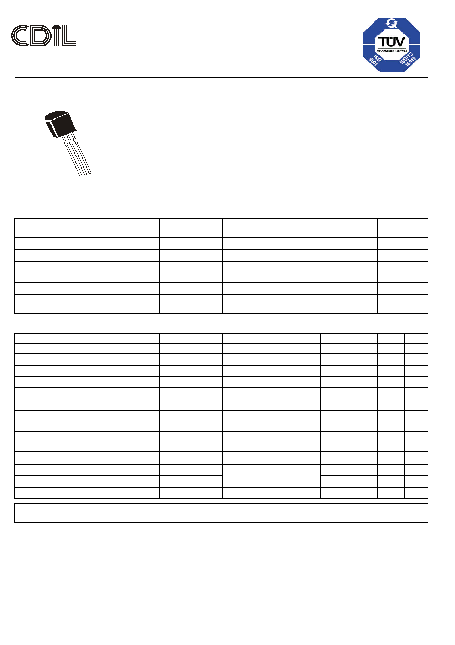
CD13002
FAST SWITCHING POWER TRANSISTOR
TO-92
Plastic Package
Compact Fluorescent Lamps (CFLS)
ABSOLUTE MAXIMUM RATING (T
a
=25∫C )
DESCRIPTION
SYMBOL
VALUE
Collector Base Voltage
V
CBO
600
Collector Emitter Voltage
V
CEO
400
Emitter Base Voltage
V
EBO
9.0
Collector Current Continuous
I
C
1.0
Peak
I
CM
1.5
Power Dissipation
P
D
1.0
Operating And Storage Junction
Temperature Range
T
j
, T
stg
- 55 to +150
ELECTRICAL CHARACTERISTICS (T
a
=25∫C unless specified otherwise)
DESCRIPTION
SYMBOL
TEST CONDITION
MIN
TYP
MAX UNIT
Collector Base Voltage
V
CBO
I
C
=1mA, I
E
=0
600
V
Collector Emitter Voltage
V
CEO
I
C
=1mA, I
B
=0
400
V
Emitter Base Voltage
V
EBO
I
E
=1mA, I
C
=0
9.0
V
Collector Cut Off Current
I
CBO
V
CB
=600V, I
E
= 0
100
µ
A
Collector Cut Off Current
I
CEO
V
CE
=400V, I
B
= 0
50
µ
A
Emitter Cut Off Current
I
EBO
V
EB
=9V, I
C
=0
100
µ
A
DC Current Gain
h
FE
V
CE
=5V, I
C
=0.1A
15
23
V
CE
=5V, I
C
=400mA
5.0
20
Collector Emitter Saturation Voltage
V
CE (sat)
I
C
=100mA, I
B
=50mA
0.05
0.11
V
I
C
=230mA, I
B
=50mA
0.12
0.24
V
Base Emitter Saturation Voltage
V
BE (sat)
I
C
=100mA, I
B
=50mA
0.82
0.88
V
Fall Time
t
f
I
C
=0.11A
0.4
µ
s
Storage Time
t
s
I
C
=0.1A, I
B1
= I
B2
=0.05A
0.07
0.9
µ
s
Transition Frequency
f
T
V
CE
=10V, I
C
=0.1A,f=1MHz
4.0
MHz
MARKING
CD
13002
CD13002Rev_1 210803E
UNIT
V
V
V
A
A
W
∫C
E C
B
Continental Device India Limited
Data Sheet
Page 1 of 4
Continental Device India Limited
An ISO/TS16949 and ISO 9001 Certified Company
CD13002
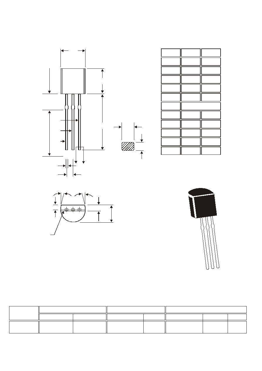
TO-92
Plastic Package
The TO-92 Package, Tape and Ammo Pack Drawings are correct as on the date of issue/revision of this Data Sheet.
The currently valid dimensions and information, may please be confirmed from the TO-92 Drawing in the Packages and
Packing Section of the Product Catalogue.
CD13002Rev_1 210803E
TO-92 Plastic Package
1
2
3
D
G
E
SEC AA
D
B
A
L
S
o
l
d
e
r
a
b
i
l
i
t
y
E
n
s
u
r
e
d
D
i
m
e
n
s
i
o
n
W
i
t
h
'
L
'
U
n
c
o
n
t
r
o
l
l
e
d
B
e
y
o
n
d
'
L
'
K
A A
1
2
3
F
F
H
C
3 2 1
M
Mold
Parting
Line
All dimensions are in mm
DIM
A
B
C
D
E
F
5 DEG
G
H
K
L
MAX.
5.33
5.20
4.19
0.55
0.50
1.40
1.40
2.082
--
1.20
M
MIN.
4.32
4.45
3.18
0.41
0.35
1.14
1.20
12.70
1.982
1.03
PIN CONFIGURATION
1. BASE
2. COLLECTOR
3. EMITTER
TO-92 Bulk
TO-92 T&A
1K/polybag
2K/ammo box
200 gm/1K pcs
645 gm/2K pcs
3" x 7.5" x 7.5"
12.5" x 8" x 1.8"
5K
2K
17" x 15" x 13.5"
17" x 15" x 13.5"
80K
32K
23 kgs
12.5 kgs
PACKAGE
Net Weight/Qty
Details
STANDARD PACK
INNER CARTON BOX
Qty
OUTER CARTON BOX
Qty
Gr Wt
Size
Size
Packing Details
Continental Device India Limited
Data Sheet
Page 2 of 4
CD13002
TO-92
Plastic Package
CD13002Rev_1 210803E
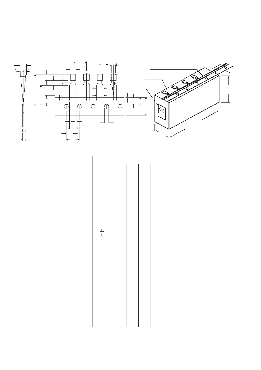
TO-92 Tape and Ammo Pack
Adhesive Tape on Top Side
Flat side
Flat Side of Transistor and
Adhesive Tape Visible
2000 pcs./Ammo Pack
Label
Carrier
Strip
186
(7.3")
332
(13
")
FEE
D
43
(1.7")
Ammo Pack Style
Tape Mechanical Data
A
A1
P
(p)
C1
C2
W2
Do
F2
F
P2
Po
F1
W1
Wo
W
H1
H2
H3
L
Ho
h1
h1
T
h
t
t1
h
ITEM
SYMBOL
SPECIFICATION
PULL - OUT FORCE
(p)
6N
MIN. NOM.
BODY WIDTH
A1
4.0
4.8
BODY HEIGHT
A
4.8
5.2
BODY THICKNESS
T
3.9
4.2
COMPONENT ALIGNMENT SIDE VIEW
h
0
1.0
COMPONENT ALIGNMENT FRONT VIEW
h1
0
1.3
COMPONENT HEIGHT
H1
23.25
LENGTH OF SNIPPED LEADS
L
11.0
TOTAL TAPE THICKNESS
t
1.2
CLINCH HEIGHT
H3
3.0
LEAD PARALLELISM
| C1 - C2 |
0.22
MAX.
PITCH OF COMPONENT
P
12.7
± 1.0
FEED HOLE PITCH
Po
12.7
± 0.3
FEED HOLE CENTRE TO
COMPONENT CENTRE
P2
6.35
± 0.4
DISTANCE BETWEEN OUTER
LEADS
F
5.08
+ 0.6
- 0.2
TAPE WIDTH
W
18
± 0.5
HOLD-DOWN TAPE WIDTH
Wo
6
± 0.2
HOLE POSITION
W1
9
+ 0.7
- 0.5
HOLD-DOWN TAPE POSITION
W2
0.5
± 0.2
LEAD WIRE CLINCH HEIGHT
Ho
16
± 0.5
FEED HOLE DIAMETER
Do
4
± 0.2
LEAD - TO - LEAD DISTANCE
F1, F2
2.54
+ 0.4
STAND OFF
H2
0.45
1.45
TOL .
- 0.1
All dimensions are in mm
3
*
4
*
5
*
1
*
*
2
At top of body
3
*
At top of body
4
*
t1 0.3 ≠ 0.6 mm
5
*
Cumulative pitch error 1.0 mm/20 pitch
1
*
*
2
To be measured at bottom of clinch
REMARKS
NOTES
1.
2.
3.
4.
5.
6.
Maximum alignment deviation between
leads will not to be greater than 0.2mm.
Maximum non-cumulative variation
between tape feed holes shall not
exceed 1 mm in 20 pitches.
Holddown tape will not exceed beyond
the edge(s) of carrier tape and there
shall be no exposure of adhesive.
There will be no more than three (3)
consecutive missing components in a
tape.
A tape trailer, having at least three feed
holes are provided after the last
component in a tape.
Splices should not interfere with the
sprocket feed holes.
Continental Device India Limited
Data Sheet
Page 3 of 4

Notes
CD13002
TO-92
Plastic Package
CD13002Rev_1 210803E
Disclaimer
The product information and the selection guides facilitate selection of the CDIL's Discrete Semiconductor Device(s) best suited for
application in your product(s) as per your requirement. It is recommended that you completely review our Data Sheet(s) so as to
confirm that the Device(s) meet functionality parameters for your application. The information furnished in the Data Sheet and on
the CDIL Web Site/CD are believed to be accurate and reliable. CDIL however, does not assume responsibility for inaccuracies or
incomplete information. Furthermore, CDIL does not assume liability whatsoever, arising out of the application or use of any CDIL
product; neither does it convey any license under its patent rights nor rights of others. These products are not designed for use in
life saving/support appliances or systems. CDIL customers selling these products (either as individual Discrete Semiconductor
Devices or incorporated in their end products), in any life saving/support appliances or systems or applications do so at their own
risk and CDIL will not be responsible for any damages resulting from such sale(s).
CDIL strives for continuous improvement and reserves the right to change the specifications of its products without prior notice.
CDIL is a registered Trademark of
Continental Device India Limited
C-120 Naraina Industrial Area, New Delhi 110 028, India.
Telephone + 91-11-2579 6150, 5141 1112 Fax + 91-11-2579 5290, 5141 1119
email@cdil.com www.cdilsemi.com
Continental Device India Limited
Data Sheet
Page 4 of 4