CMT2N7002E
S
MALL
S
IGNAL
MOSFET
2004/11/05
Preliminary
Rev. 2
Champion Microelectronic Corporation
Page 1
GENERAL DESCRIPTION
FEATURES
This N-Channel enhancement mode field effect transistor is
produced using high cell density, DMOS technology. These
products have been designed to minimize on-state
resistance while provide rugged, reliable, and fast switching
performance. This product is particularly suited for low
voltage, low current applications such as small servo motor
control, power MOSFET gate drivers, and other switching
applications.
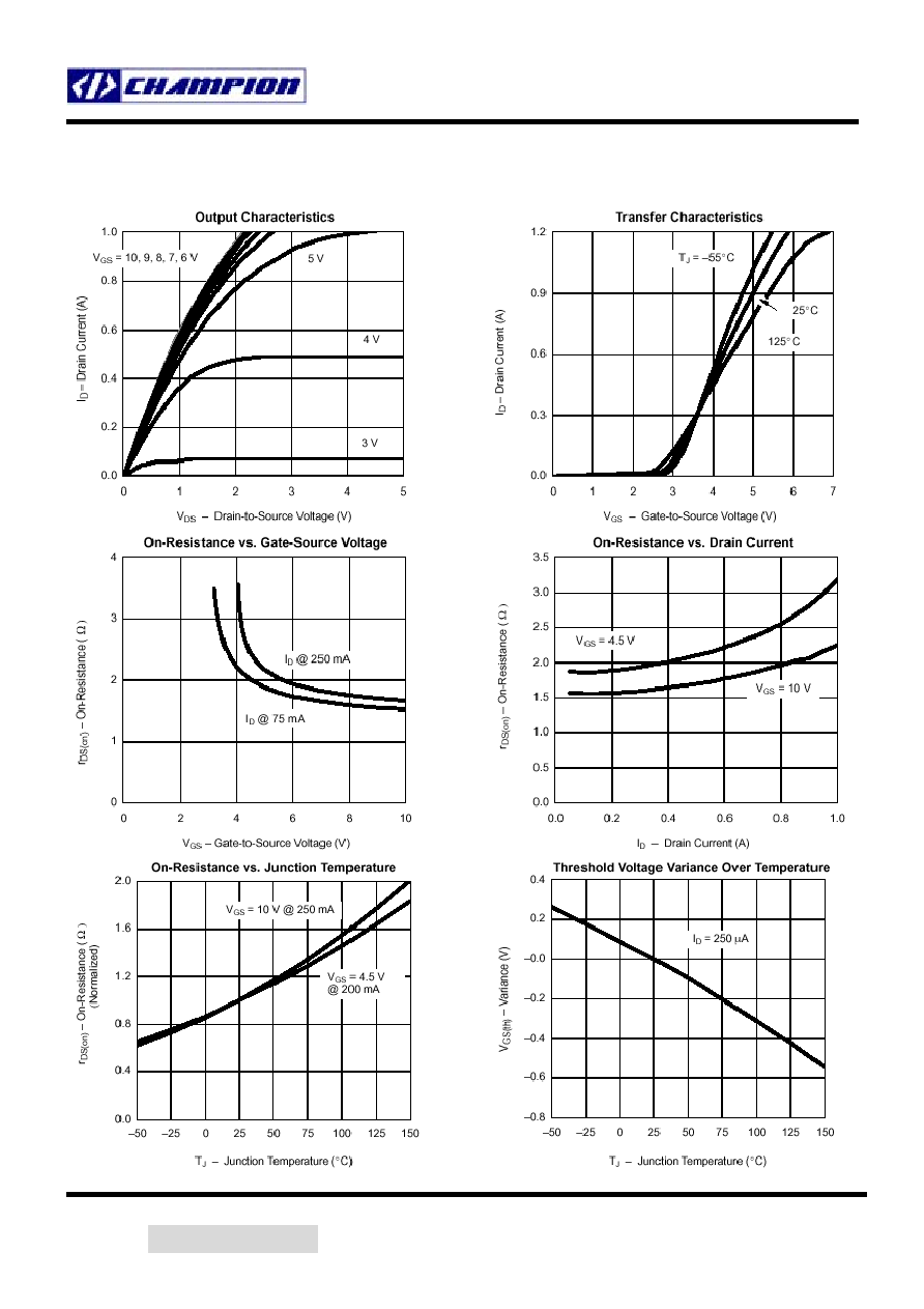
Low On-Resistance: 3
Low Threshold: 2V (typ.)
Low Input Capacitance: 25pF
Fast Switching Speed: 7.5ns
Low Input and Output Leakage
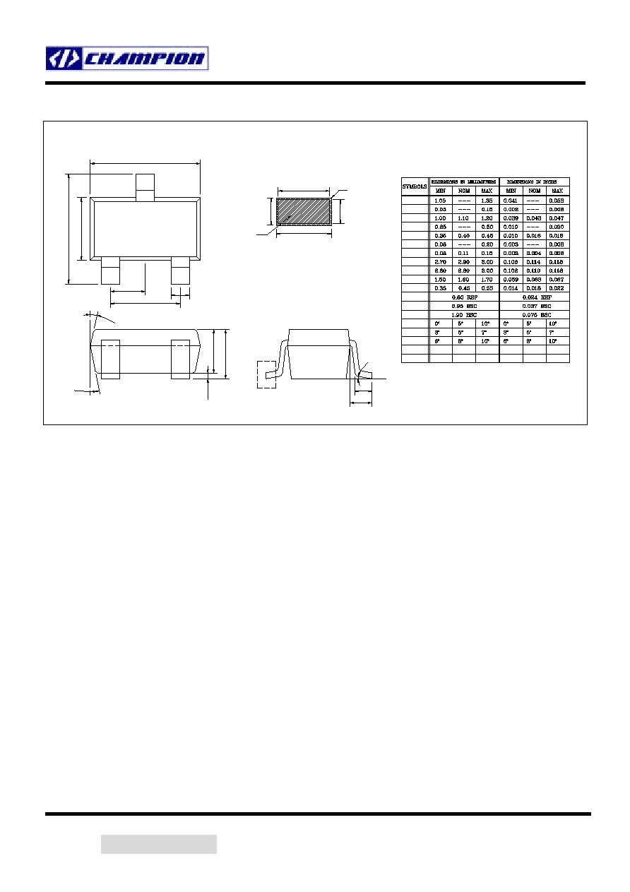
PIN CONFIGURATION
SYMBOL
SOT-23
Top View
1
3
2
GA
T
E
DRAI
N
SO
URCE
D
S
G
N-Channel MOSFET
ORDERING INFORMATION
Part Number
Package
CMT2N7002E SOT-23
CMT2N7002EG* SOT-23
*Note:
G : Suffix for Pb Free Product
ABSOLUTE MAXIMUM RATINGS
Rating Symbol
Value
Unit
Drain Source Voltage
V
DSS
60 V
Drain-Gate Voltage (R
GS
= 1.0M) V
DGR
60 V
T
A
= 25 240
Continuous Drain Current (T
J
= 150)
T
A
= 70
I
D
190
mA
Pulsed Drain Current (Note 1)
I
DM
1300 mA
Gate-to-Source Voltage
V
GS
±20 V
T
A
= 25 0.35
Total Power Dissipation
T
A
= 70
P
D
0.22
W
Operating and Storage Temperature Range
T
J
, T
STG
-55 to 150
Thermal Resistance Junction to Ambient
JA
357
/W
Note1: Pulse Width limited by maximum junction temperature.
CMT2N7002E
S
MALL
S
IGNAL
MOSFET
2004/11/05
Preliminary
Rev. 2
Champion Microelectronic Corporation
Page 2
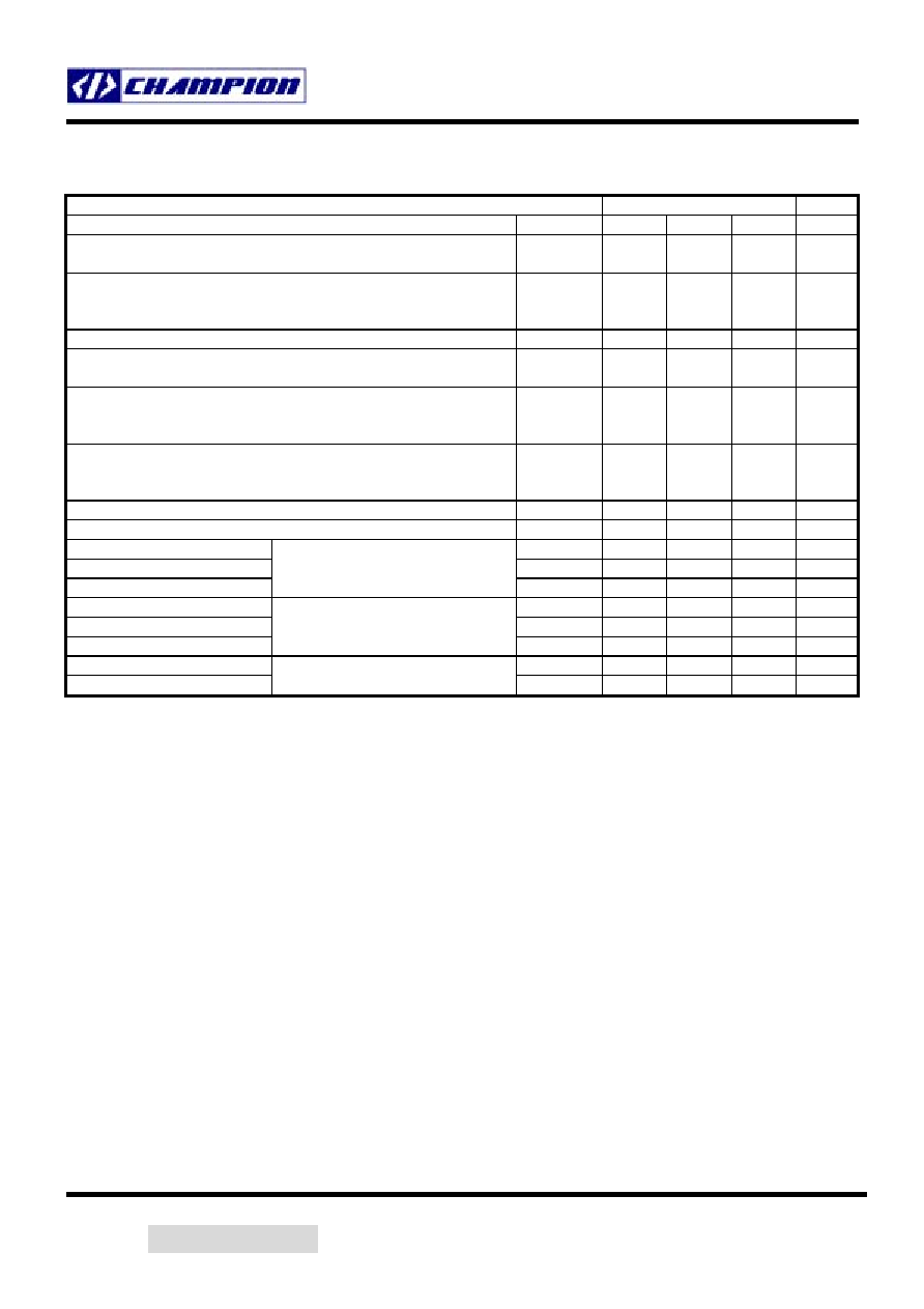
ELECTRICAL CHARACTERISTICS
Unless otherwise specified, T
J
= 25.
CMT2N7002E
Characteristic Symbol
Min
Typ
Max
Units
Drain-Source Breakdown Voltage
(V
GS
= 0 V, I
D
= 10 A)
V
(BR)DSS
60 68 V
Zero Gate Voltage Drain Current
(V
DS
= 60 V, V
GS
= 0 V)
(V
DS
= 60 V, V
GS
= 0 V, T
C
= 125)
I
DSS
1.0
500
A
A
Gate Body Leakage (V
DS
= 0 V, V
GS
= ±15 V)
I
GSS
±10
nA
Gate Threshold Voltage *
(V
DS
= V
GS
, I
D
= 250 A)
V
GS(th)
1.0 2.0 2.5 V
On-State Drain Current (Note 2)
(V
DS
= 7.5 V, V
GS
= 10V)
(V
DS
= 10 V, V
GS
= 4.5V)
I
d(on)
800
350
1900
450
mA
Static Drain-Source On-Resistance (Note 2)
(V
GS
= 10 V, I
D
= 0.25A)
(V
GS
= 4.5 V, I
D
= 0.2A)
R
DS(on)
1.9
3.5
3
4
Diode Forward On-Voltage (I
S
= 200 mA, VGS = 0V)
V
SD
0.85
1.2
V
Forward Transconductance (V
DS
= 15 V, I
D
= 200mA) (Note 2)
g
FS
150
260
mmhos
Total Gate Charge
Q
g
0.4
0.6
nC
Gate-Source Charge
Q
gs
0.06 nC
Gate-Drain Charge
(V
DS
= 25 V, V
GS
= 0 V,
f = 1.0 MHz) (Note 1)
Q
gd
0.06 nC
Input Capacitance
C
iss
21
pF
Output Capacitance
C
oss
7
pF
Reverse Transfer Capacitance
(V
DS
= 25 V, V
GS
= 0 V,
f = 1.0 MHz) (Note 1)
C
rss
2.5 pF
Turn-On Delay Time (Note 1,3)
t
d(on)
13
20
ns
Turn-Off Delay Time (Note 1,3)
(V
DD
= 10 V, I
D
= 250 mA,
V
GEN
= 10 V, R
G
= 10, R
L
= 40)
t
d(off)
18
25
ns
Note 1: For Design Aid Only, not subject to production testing.
Note 2: Pulse test: PW <= 300µs duty cycle <=2%
Note 3: Switching time is essentially independent of operating temperature.