 | ÐлекÑÑоннÑй компоненÑ: CMT70N03 | СкаÑаÑÑ:  PDF PDF  ZIP ZIP |
Äîêóìåíòàöèÿ è îïèñàíèÿ www.docs.chipfind.ru
CMT70N03
N-C
HANNEL
Logic Level Power M
OSFET
2004/04/13 Champion Microelectronic Corporation
Page
1
APPLICATION
FEATURES
Buck Converter High Side Switch
Other Applications
V
DSS
R
DS(ON)
Typ.
I
D
30V 6.6m 71A
Low ON Resistance
Low Gate Charge
Peak Current vs Pulse Width Curve
Inductive Switching Curves
Improved UIS Ruggedness
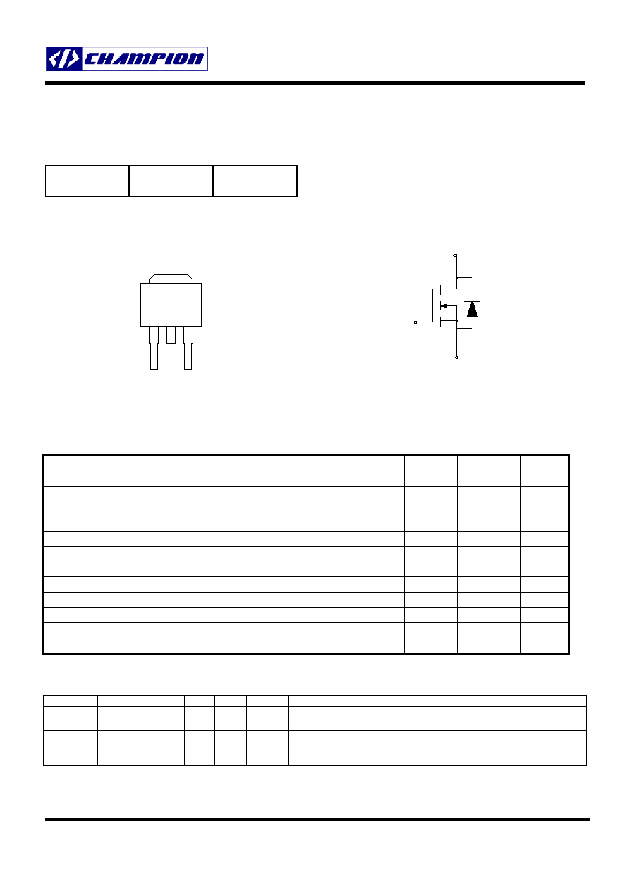
PIN CONFIGURATION
SYMBOL
TO-252
Front View
1
2
3
GA
T
E
DR
AI
N
S
O
UR
CE
D
S
G
N-Channel MOSFET
ABSOLUTE MAXIMUM RATINGS
Rating Symbol
Value
Unit
Drain to Source Voltage (Note 1)
V
DSS
30 V
Drain to Current Continuous Tc = 25, V
GS
@10V (Note 2)
Continuous Tc = 100, V
GS
@10V (Note 2)
Pulsed Tc = 25, V
GS
@10V (Note 3)
I
D
I
D
I
DM
71
45
284
A
Gate-to-Source Voltage Continue
V
GS
±20 V
Total Power Dissipation
Derating Factor above 25
P
D
66
0.53
W
W/
Peak Diode Recovery dv/dt (Note 4)
dv/dt
3.0
V/ns
Operating Junction and Storage Temperature Range
T
J
, T
STG
-55 to 150
Single Pulse Avalanche Energy
E
AS
TBD mJ
Maximum Lead Temperature for Soldering Purposes
T
L
300
Maximum Package Body for 10 seconds
T
PKG
260
THERMAL RESISTANCE
Symbol Parameter Min
Typ
Max
Units
Test
Conditions
R
JC
Junction-to-case
1.9 /W Water cooled heatsink, P
D
adjusted for a peak junction
temperature of +150
R
JA
Junction-to-ambient
(PCB Mount)
50 /W Minimum pad area, 2-oz copper, FR-4 circuit board, double
sided
R
JA
Junction-to-ambient
62
/W 1 cubic foot chamber, free air
CMT70N03
N-C
HANNEL
Logic Level Power M
OSFET
2004/04/13 Champion Microelectronic Corporation
Page
2
ORDERING INFORMATION
Part Number
Package
CMT70N03 TO-252
ELECTRICAL CHARACTERISTICS
Unless otherwise specified, T
J
= 25.
CMT70N03
Characteristic Symbol
Min
Typ
Max
Units
OFF Characteristics
Drain-to-Source Breakdown Voltage
(V
GS
= 0 V, I
D
= 250 µA)
V
DSS
30
V
Breakdown Voltage Temperature Coefficient,
(Reference to 25
,
I
D
= 1mA)
V
DSS
/T
J
0.05 V/
Drain-to-Source Leakage Current
(V
DS
= 30 V, V
GS
= 0 V, T
J
= 25)
(V
DS
= 24 V, V
GS
= 0 V, T
J
= 125)
I
DSS
1
10
µA
Gate-to-Source Forward Leakage
(V
GS
= 20 V)
I
GSS
100
nA
Gate-to-Source Reverse Leakage
(V
GS
= -20 V)
I
GSS
-100
nA
ON Characteristics
Gate Threshold Voltage,
(V
DS
= V
GS
, I
D
= 250 µA)
V
GS(th)
1.0 3.0 V
Static Drain-to-Source On-Resistance, (Note 5)
(V
GS
= 10 V, I
D
= 15A)
(V
GS
= 4.5 V, I
D
= 12A)
R
DS(on)
6.6
12
8.0
m
Forward Transconductance (V
DS
= 20V, I
D
= 12A) (Note 5)
g
FS
30 S
Dynamic Characteristics
Input Capacitance
C
iss
2600 pF
Output Capacitance
C
oss
480 pF
Reverse Transfer Capacitance
(V
DS
= 15 V, V
GS
= 0 V,
f = 1.0 MHz)
C
rss
230 pF
Total Gate Charge (V
GS
= 10 V)
Q
g
50 nC
Total Gate Charge (V
GS
= 4.5 V)
Q
g
25 nC
Gate-to-Source Charge
Q
gs
7.5 nC
Gate-to-Drain Charge
(V
DS
= 15 V, I
D
= 12 A) (Note5, 6)
Q
gd
8.5 nC
Resistive Switching Characteristics
Turn-On Delay Time
t
d(on)
TBD ns
Rise Time
t
r
TBD ns
Turn-Off Delay Time
t
d(off)
TBD ns
Fall Time
(V
DD
= 15 V, I
D
= 15 A,
V
GS
= 10 V, R
G
= TBD)
(Note 5,6)
t
f
TBD ns
Source-Drain Diode Characteristics
Continuous Source Current (Body
Diode )
I
S
71
A
Pulse Source Current (Body Diode)
Integral pn-diode in MOSFET(Note 2)
I
SM
284
A
Forward On-Voltage
(I
S
= 12 A, V
GS
= 0 V)
V
SD
1.0
V
Forward Turn-On Time
t
rr
30 ns
Reverse Recovery Charge
(I
F
= 12 A, V
GS
= 0 V,
d
i
/d
t
= 100A/µs) (Note 5)
Q
rr
40
nC
CMT70N03
N-C
HANNEL
Logic Level Power M
OSFET
2004/04/13 Champion Microelectronic Corporation
Page
3
Note 1: T
J
= +25 to 150
Note 2: Current is calculated based upon maximum allowable junction temperature.
Package current limitation is 30A.
Note 3: Repetitive rating; pulse width limited by maximum junction temperature.
Note 4: I
SD
= 12.0A, di/dt <200A/µs, V
DD
<BV
DSS
, T
J
= +150
Note 5: Pulse width < 250µs; duty cycle < 2%
Note 6: Essentially independent of operating temerpature.
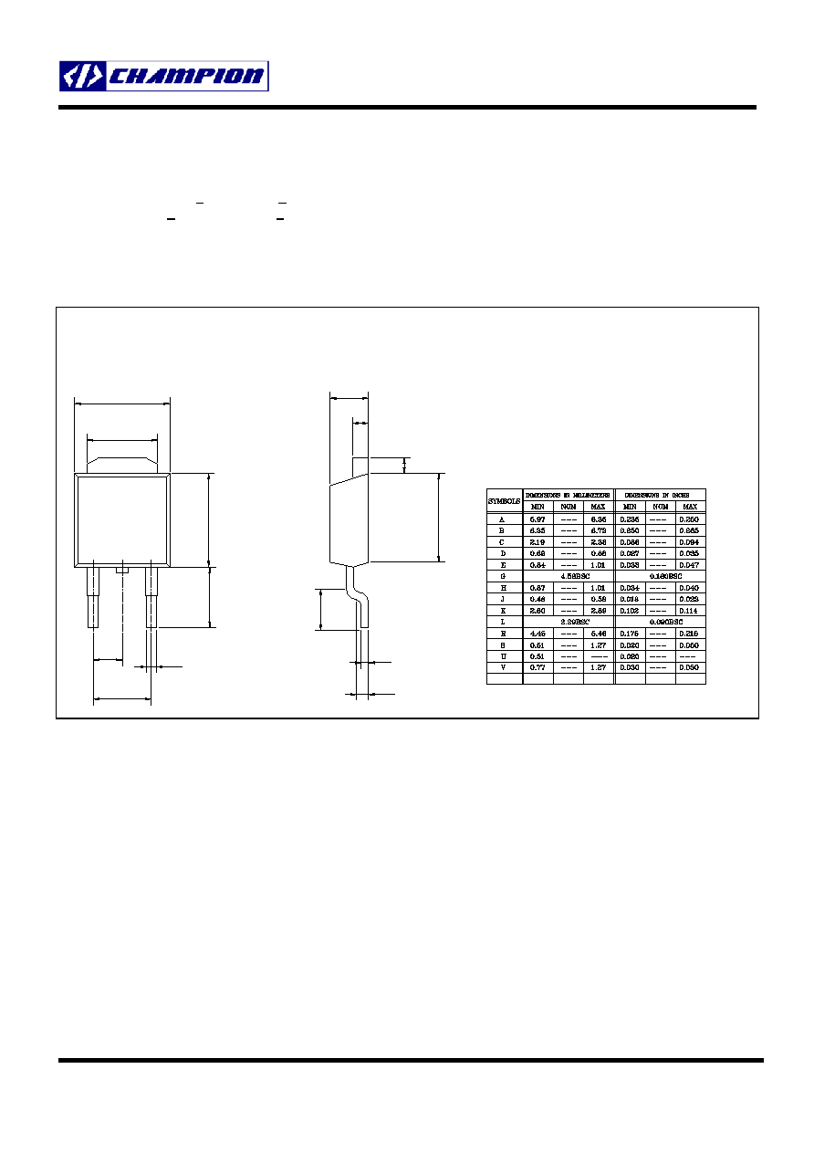
PACKAGE DIMENSION
TO-252
1
2
3
4
L
E
C
A
V
J
U
H
D
R
B
S
K
G
PIN 1: GATE
PIN 2: DRAIN
PIN 3: SOURCE

CMT70N03
N-C
HANNEL
Logic Level Power M
OSFET
2004/04/13 Champion Microelectronic Corporation
Page
4
IMPORTANT NOTICE
Champion Microelectronic Corporation (CMC) reserves the right to make changes to its products or to discontinue any
integrated circuit product or service without notice, and advises its customers to obtain the latest version of relevant information
to verify, before placing orders, that the information being relied on is current.
A few applications using integrated circuit products may involve potential risks of death, personal injury, or severe property or
environmental damage. CMC integrated circuit products are not designed, intended, authorized, or warranted to be suitable for
use in life-support applications, devices or systems or other critical applications. Use of CMC products in such applications is
understood to be fully at the risk of the customer. In order to minimize risks associated with the customer's applications, the
customer should provide adequate design and operating safeguards.
HsinChu Headquarter
Sales & Marketing
5F-1, No. 11, Park Avenue II,
Science-Based Industrial Park,
HsinChu City, Taiwan
11F, No. 306-3, SEC. 1, Ta Tung Road,
Hsichih, Taipei Hsien 221, Taiwan
T E L : +886-3-567 9979
T E L : +886-2-8692 1591
FAX: +886-3-567 9909
FAX: +886-2-8692 1596
Document Outline