 | –≠–ª–µ–∫—Ç—Ä–æ–Ω–Ω—ã–π –∫–æ–º–ø–æ–Ω–µ–Ω—Ç: CP2101 | –°–∫–∞—á–∞—Ç—å:  PDF PDF  ZIP ZIP |
DS014-1.0 AUG03
CYGNAL Integrated Products, Inc.
© 2003
Page 1
Preliminary
Single-Chip USB to UART Bridge
CP2101
SINGLE-CHIP USB to UART DATA TRANSFER
-
Integrated USB Transceiver; No External Resistors
Required
-
Integrated Clock; No External Crystal Required
-
Integrated 512-Byte EEPROM for Vendor ID, Product ID,
Serial Number, Power Descriptor, Release Number and
Product Description Strings
-
On-Chip Power-On Reset Circuit
-
On-Chip Voltage Regulator: 3.3V Output
USB FUNCTION CONTROLLER
-
USB Specification 2.0 Compliant; Full Speed (12 Mbps)
-
USB suspend states supported via SUSPEND pins
ASYNCHRONOUS SERIAL DATA BUS (UART)
-
All Handshaking and Modem Interface Signals
-
Data Formats Supported:
∑
Data Bits: 8
∑
Stop Bits: 1, 2
∑
Parity: Odd, Even, No Parity
-
Baud Rates: 300bps to 921.6kbps
-
512 Byte Receive Buffer; 512 Byte Transmit Buffer
-
Hardware or X-On / X-Off Handshaking Supported
-
Event Character and Line Break Condition Support
VIRTUAL COM PORT DEVICE DRIVERS
-
Works with Existing COM Port PC Applications
-
Royalty-Free Distribution License
-
Windows 98/Me/2000/XP
-
MAC OS-9
-
MAC OS-X
-
Windows CE *
-
Linux 2.40 and greater *
* (Contact factory for availability)
EXAMPLE APPLICATIONS
-
Upgrade of RS-232 Legacy Devices to USB
-
Cellular Phone USB Interface Cable
-
PDA USB Interface Cable
-
USB to RS-232 Serial Adapter
SUPPLY VOLTAGE
-
Self-powered: 3.0V to 3.6V
-
USB Bus Powered: 4.0V to 5.25V
PACKAGE
-
28-pin MLP (5mm X 5mm)
TEMPERATURE RANGE: -40∞C TO +85∞C
CP2101
3.3V
Voltage
Regulator
48MHz
Oscillator
IN
OUT
/SUSPEND
SUSPEND
11
12
REGIN
7
GND
3
/RST
9
D+
4
D-
5
8
C1
4.7uF
TANT
C2
1uF
C3
0.1uF
UART
RI
DCD
CTS
RTS
RXD
TXD
DSR
DTR
2
1
28
27
26
25
24
23
2
3
External RS-232
transceiver or
UART circuitry
(to external circuitry
for USB suspend
states)
VBUS
D-
D+
GND
4
5
6
USB
CONNECTOR
6
1
VDD
VBUS
USB Function
Controller
USB
Transceiver
512B
Xmit
Buffer
512B
Rcv
Buffer
512B
EEPROM
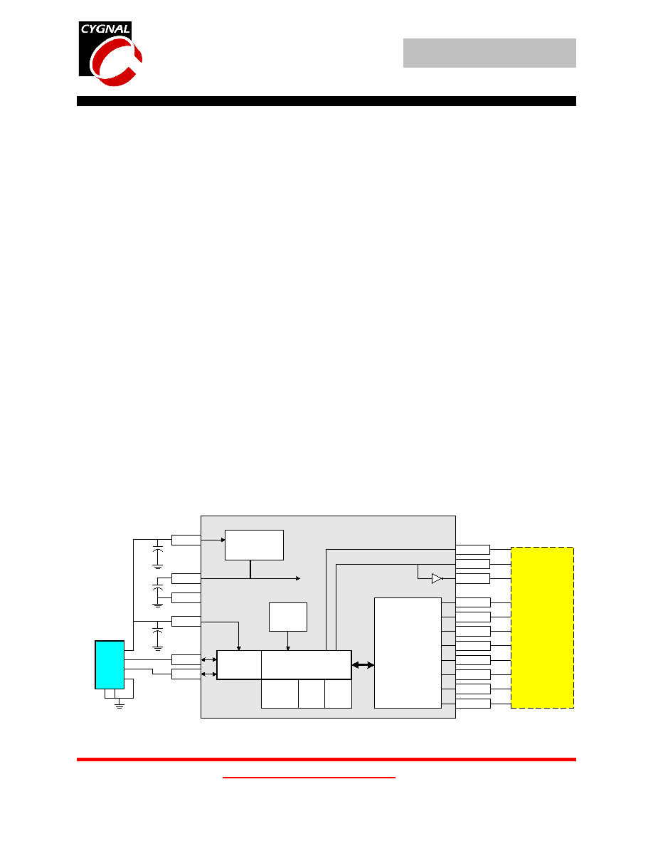
Example Circuit Diagram

Preliminary
Page 2
DS014-1.0 AUG03
© 2003 Cygnal Integrated Products, Inc.
CP2101
Notes

© 2003 Cygnal Integrated Products, Inc.
DS014-1.0 AUG03
Page 3
Preliminary
CP2101
TABLE OF CONTENTS
1. SYSTEM OVERVIEW ...........................................................................................................5
2. ABSOLUTE MAXIMUM RATINGS....................................................................................5
Table 2.1. Absolute Maximum Ratings* ..................................................................................5
3. GLOBAL DC ELECTRICAL CHARACTERISTICS ........................................................6
Table 3.1. Global DC Electrical Characteristics.......................................................................6
4. PINOUT AND PACKAGE DEFINITIONS..........................................................................6
Table 4.1. Pin Definitions for the CP2101................................................................................6
Figure 4.1. MLP-28 Pinout Diagram (Top View) .....................................................................7
Figure 4.2. MLP-28 Package Drawing ......................................................................................8
Table 4.2. MLP-28 Package Dimensions .................................................................................8
Figure 4.3. Typical MLP-28 Landing Diagram.........................................................................9
Figure 4.4. Typical MLP-28 Solder Mask...............................................................................10
5. USB FUNCTION CONTROLLER AND TRANSCEIVER ..............................................11
6. ASYNCHRONOUS SERIAL DATA BUS (UART) INTERFACE...................................11
Table 6.1. Data Formats and Baud Rates................................................................................11
7. INTERNAL EEPROM..........................................................................................................12
Table 7.1. Default USB Configuration Data...........................................................................12
8. VIRTUAL COM PORT DEVICE DRIVERS.....................................................................12
9. VOLTAGE REGULATOR...................................................................................................13
Table 9.1. Voltage Regulator Electrical Specifications ..........................................................13

Preliminary
Page 4
DS014-1.0 AUG03
© 2003 Cygnal Integrated Products, Inc.
CP2101
Notes
© 2003 Cygnal Integrated Products, Inc.
DS014-1.0 AUG03
Page 5
Preliminary
CP2101
1.
SYSTEM OVERVIEW
The CP2101 is a highly-integrated USB-to-UART Bridge Controller providing a simple solution for updating RS232
designs to USB using a minimum of components and PCB space. The CP2101 includes a USB 2.0 full-speed
function controller, USB transceiver, oscillator, EEPROM and asynchronous serial data bus (UART) with full modem
control signals in a compact 5mm X 5mm MLP-28 package. No other external USB components are required.
The on-chip EEPROM may be used to customize the USB Vendor ID, Product ID, Product Description String, Power
Descriptor, Device Release Number and Device Serial Number as desired for OEM applications. The EEPROM is
programmed on-board via the USB allowing the programming step to be easily integrated into the product
manufacturing and testing process.
Royalty-free Virtual COM Port (VCP) device drivers provided by Cygnal allow a CP2101-based product to appear as
a COM port to PC applications. The CP2101 UART interface implements all RS232 signals, including control and
handshaking signals, so existing system firmware does not need to be modified. In many existing RS232 designs, all
that is required to update the design from RS232 to USB is to replace the RS232 level-translator with the CP2101.
An evaluation kit for the CP2101 (Part Number: CP2101EK) is available. It includes a CP2101-based USB-to-
UART/RS232 evaluation board, a complete set of VCP device drivers, USB and RS232 cables and full
documentation. Contact any of Cygnal's sales representatives or go to www.cygnal.com to order the CP2101
Evaluation Kit.
2.
ABSOLUTE MAXIMUM RATINGS
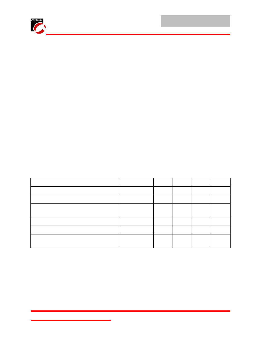
Table 2.1. Absolute Maximum Ratings
*
PARAMETER
CONDITIONS
MIN
TYP
MAX
UNITS
Ambient temperature under bias
-55
125
∞C
Storage Temperature
-65
150
∞C
Voltage on any I/O Pin or /RST with respect to
GND
-0.3
5.8
V
Voltage on VDD with respect to GND
-0.3
4.2
V
Maximum Total current through VDD and GND
500
mA
Maximum output current sunk by /RST or any
I/O pin
100
mA
*
Note: stresses above those listed under "Absolute Maximum Ratings" may cause permanent damage to the device.
This is a stress rating only and functional operation of the devices at those or any other conditions above those indi-
cated in the operation listings of this specification is not implied. Exposure to maximum rating conditions for
extended periods may affect device reliability.