Äîêóìåíòàöèÿ è îïèñàíèÿ www.docs.chipfind.ru

High Speed Super Low Power SRAM
256K-Word By 8 Bit
CS18LV20483
1
Rev. 1.0
Chiplus reserves the right to change product or specification without notice.
Revision History
Rev. No. History Issue
Date
Remark
1.0 Initial
issue
Jan.26,2005
High Speed Super Low Power SRAM
256K-Word By 8 Bit
CS18LV20483
2
Rev. 1.0
Chiplus reserves the right to change product or specification without notice.
GENERAL DESCRIPTION
The CS18LV20483 is a high performance, high speed, and super low power CMOS Static
Random Access Memory organized as 262,144 words by 8 bits and operates from a wide range of
2.7 to 3.6V supply voltage. Advanced CMOS technology and circuit techniques provide both high
speed and low power features with a typical CMOS standby current of 0.50uA and maximum
access time of 55/70ns in 3.0V operation. Easy memory expansion is provided by an active LOW
chip enable inputs (/CE1,CE2) and active LOW output enable (/OE) and three-state output drivers.
The CS18LV20483 has an automatic power down feature, reducing the power consumption
significantly when chip is deselected. The CS18LV20483 is available in JEDEC standard 32-pin
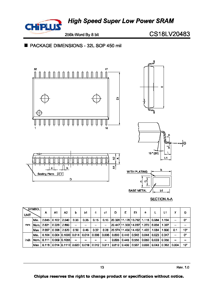
sTSOP (8x13.4 mm), TSOP (8x20mm), TSOP (II) (400mil) and SOP (450 mil) packages.
.
FEATURES
Low operation voltage : 2.7 ~ 3.6V
Ultra low power consumption : 2mA1MHz (Max.) operating current
0.50 uA (Typ.) CMOS standby current
High speed access time : 55/70ns (Max.) at Vcc = 3.0V.
Automatic power down when chip is deselected.
Three state outputs and TTL compatible
Data retention supply voltage as low as 1.5V.
Easy expansion with /CE and /OE options.
Product Family
Product Family
Operating
Temp
Vcc. Range
Speed (ns) Standby (Typ.) Package Type
32 SOP
32 STSOP
32 TSOP
32 TSOP (II)
0~70
o
C 2.7~3.6 55/70
0.50 uA
(Vcc = 3.0V)
Dice
32 SOP
32 STSOP
32 TSOP
32 TSOP (II)
CS18LV20483
-40~85
o
C 2.7~3.6 55/70
0.8 uA
(Vcc= 3.0V)
Dice

High Speed Super Low Power SRAM
256K-Word By 8 Bit
CS18LV20483
3
Rev. 1.0
Chiplus reserves the right to change product or specification without notice.
PIN CONFIGURATIONS
FUNCTIONAL BLOCK DIAGRAM

High Speed Super Low Power SRAM
256K-Word By 8 Bit
CS18LV20483
4
Rev. 1.0
Chiplus reserves the right to change product or specification without notice.
PIN DESCRIPTIONS
Name
Type
Function
A0 A17
Input
Address inputs for selecting one of the 262,144 x 8 bit words in the RAM
/CE1, CE2
Input
/CE1 is active LOW and CE2 is active HIGH. Both chip enables must be
active when data read from or write to the device. If either chip enable is
not active, the device is deselected and in a standby power down mode.
The DQ pins will be in high impedance state when the device is
deselected.
/WE
Input
The Write enable input is active LOW. It controls read and write
operations. With the chip selected, when /WE is HIGH and /OE is LOW,
output data will be present on the DQ pins, when /WE is LOW, the data
present on the DQ pins will be written into the selected memory location.
/OE
Input
The output enable input is active LOW. If the output enable is active
while the chip is selected and the write enable is inactive, data will be
present on the DQ pins and they will be enabled. The DQ pins will be in
the high impedance state when /OE is inactive.
DQ0~DQ7
I/O
These 8 bi-directional ports are used to read data from or write data into
the RAM.
Vcc
Power
Power Supply
Gnd
Power
Ground
NC
No
connection
TRUTH TABLE
MODE
/CE1
CE2
/WE
/OE
DQ0~7
Vcc Current
H
X
X
X
Standby
X
L X L
High Z
I
CCSB
, I
CCSB1
Output
Disabled
L
H H
H High
Z I
CC
Read
L H H
L
D
OUT
I
CC
Write
L H L
X
D
IN
I
CC

High Speed Super Low Power SRAM
256K-Word By 8 Bit
CS18LV20483
5
Rev. 1.0
Chiplus reserves the right to change product or specification without notice.
ABSOLUTE MAXIMUM RATINGS (1)
Symbol
Parameter
Rating
Unit
V
TERM
Terminal Voltage with Respect to GND
-0.5 to Vcc+0.5
V
T
BIAS
Temperature Under Bias
-40 to +125
O
C
T
STG
Storage Temperature
-60 to +150
O
C
P
T
Power Dissipation
1.0
W
I
OUT
DC Output Current
25
mA
1.
Stresses greater than those listed under ABSOLUTE MAXIMUM RATINGS may cause
permanent damage to the device. This is a stress rating only and functional operation of the device
at these or any other conditions above those indicated in the operational sections of this
specification is not implied. Exposure to absolute maximum rating conditions for extended periods
may affect reliability.
OPERATING RANGE
Range
Ambient Temperature
Vcc
Commercial
0~70
o
C
2.7V ~ 3.6V
Industrial
-40~85
o
C
2.7V ~ 3.6V
1. Overshoot : Vcc +2.0V in case of pulse width 20ns.
2. Undershoot : - 2.0V in case of pulse width 20ns.
3. Overshoot and undershoot are sampled, not 100% tested.
CAPACITANCE
(1)
(TA = 25
o
C, f =1.0 MHz)
Symbol
Parameter
Conditions
MAX.
Unit
C
IN
Input Capacitance
V
IN
=0V
6 pF
C
DQ
Input/Output Capacitance
V
I/O
=0V
8 pF
1. This parameter is guaranteed and not tested.

High Speed Super Low Power SRAM
256K-Word By 8 Bit
CS18LV20483
6
Rev. 1.0
Chiplus reserves the right to change product or specification without notice.
DC ELECTRICAL CHARACTERISTICS
( TA = 0 to + 70
o
C , Vcc = 3.0V )
Parameter
Name
Parameter
Test Conduction
MIN
TYP
(1)
MAX Unit
V
IL
Guaranteed Input Low
Voltage
(2)
-0.5 0.8 V
V
IH
Guaranteed Input High
Voltage
(2)
2.0 Vcc+0.2
V
I
IL
Input Leakage Current V
CC
=MAX, V
IN
=0 to V
CC
-1 1
uA
I
OL
Output Leakage
Current
V
CC
=MAX, /CE=V
IN
, or
/OE=V
IN
, V
IO
=0V to V
CC
-1 1
uA
V
OL
Output Low Voltage
V
CC
=MAX, I
OL
= 2mA
0.4
V
V
OH
Output High Voltage
V
CC
=MIN, I
OH
= -1mA
2.4
V
I
CC
Operating Power
Supply Current
/CE=V
IL
, I
DQ
=0mA, F=F
MAX
(3)
25
mA
I
CCSB
Standby Supply - TTL /CE=V
IH
, I
DQ
=0mA,
1
mA
I
CCSB1
Standby Current
-CMOS
/CEV
CC
-0.2V, V
IN
V
CC
-0.2V or V
IN
0.2V
0.5 4
uA
1. Typical characteristics are at TA = 25
o
C.
2. These are absolute values with respect to device ground and all overshoots due to system or
tester notice are included.
3.
Fmax = 1/t
RC
.
DATA RETENTION CHARACTERISTICS
( TA =
0 to + 70
o
C
)
Parameter Name
Parameter
Test Conduction
MIN TYP
MAX Unit
V
DR
V
CC
for Data Retention /CEV
CC
-0.2V,
V
IN
V
CC
-0.2V or V
IN
0.2V
1.5 V
I
CCDR
Data Retention Current /CEV
CC
-0.2V, V
CC=
1.5V
V
IN
V
CC
-0.2V or V
IN
0.2V
0.3 2 uA
T
CDR
Chip Deselect to Data
Retention Time
0 ns
t
R
Operation Recovery
Time
See Retention Waveform
t
RC
(1)
ns
1. Read Cycle Time.

High Speed Super Low Power SRAM
256K-Word By 8 Bit
CS18LV20483
7
Rev. 1.0
Chiplus reserves the right to change product or specification without notice.
LOW Vcc DATA RETENTION WAVEFORM 1 ( /CE1 Controlled )
LOW Vcc DATA RETENTION WAVEFORM 2 ( CE2
Controlled )
AC TEST CONDITIONS
KEY TO SWITCHING WAVEFORMS
Input Pulse Levels
Vcc/0V
WAVEFORMS
INPUTS
OUTPUTS
Input Rise and Fall Times
5ns
MUST BE STEADY MUST BE STEADY
Input and Output Timing
Reference Level
0.5Vcc
Output Load
See FIGURE 1A
and 1B
MAY CHANGE
FROM H TO L
WILL BE CHANGE FROM H
TO L
MAY CHANGE
FROM L TO H
WILL BE CHANGE FROM L
TO H
DON'T CARE ANY
CHANGE
PERMITTED
CHANGE STATE
UNKNOWN
DOES NOT APPLY
CENTER LINE IS HIGH
IMPEDANCE OFF STATE

High Speed Super Low Power SRAM
256K-Word By 8 Bit
CS18LV20483
8
Rev. 1.0
Chiplus reserves the right to change product or specification without notice.
AC TEST LOADS AND WAVEFORMS
FIGURE 1A
FIGURE 1B
667
TERMINAL EQUIVALENT
OUTPUT
1.73V
GND
V
CC
5ns
5ns
10%
90%
90%
10%
ALL INPUT PULSES
FIGURE 2
AC ELECTRICAL CHARACTERISTICS
( TA =
0 to + 70
o
C
, Vcc = 3.3V )
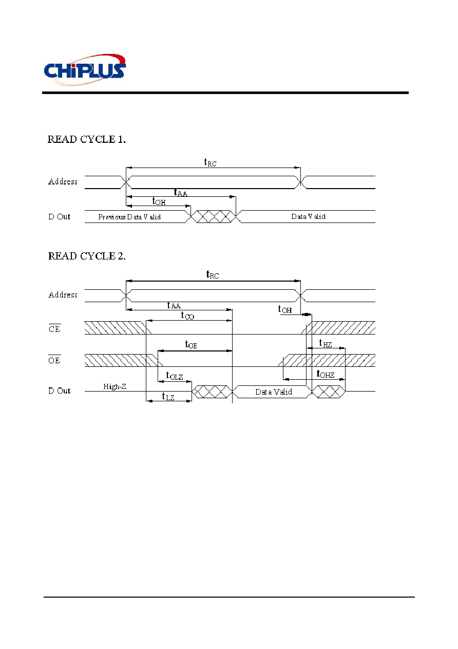
< READ CYCLE >
-55
-70
JEDEC
Parameter
Name
Parameter
Name
Description
MIN MAX MIN MAX
Unit
t
AVAX
t
RC
Read Cycle Time
55
70
ns
t
AVQV
t
AA
Address Access Time
55
70
ns
t
ELQV
t
CO
Chip Select Access Time
55
70
ns
t
GLQV
t
OE
Output Enable to Output Valid
25
35
ns
t
ELQX
t
LZ
Chip Select to Output Low Z
10
10
ns
t
GLQX
t
OLZ
Output Enable to Output in Low Z
5
5
ns
t
EHQZ
t
CHZ
Chip Deselect to Output in High Z
0
20
0
25
ns
t
GHQZ
t
OHZ
Output Disable to Output in High Z
0
20
0
25
ns
t
AXOX
t
OH
Out Disable to Address Change
10
10
ns
High Speed Super Low Power SRAM
256K-Word By 8 Bit
CS18LV20483
9
Rev. 1.0
Chiplus reserves the right to change product or specification without notice.
SWITCHING WAVEFORMS (READ CYCLE)
NOTES:
1.
t
HZ
and t
OHZ
are defined as the outputs achieve the open circuit conditions and are not
referenced to output voltage levels.
2. At any given temperature and voltage condition, tHZ(Max.) is less than tLZ(Min.) both
for a given device and from device to device interconnection.

High Speed Super Low Power SRAM
256K-Word By 8 Bit
CS18LV20483
10
Rev. 1.0
Chiplus reserves the right to change product or specification without notice.
AC ELECTRICAL CHARACTERISTICS (
TA =
0 to + 70
o
C
, Vcc = 3.3V )
< WRITE CYCLE >
-55
-70
JEDEC
Parameter
Name
Parameter
Name
Description
MIN MAX MIN MAX
Unit
t
AVAX
t
WC
Write Cycle Time
55 70 ns
t
E1LWH
t
CW
Chip Select to End of Write
45 60 ns
t
AVWL
t
AS
Address Setup Time
0 0 ns
t
AVWH
t
AW
Address Valid to End of Write
45 60 ns
t
WLWH
t
WP
Write Pulse Width
40 50 ns
t
WHAX
t
WR
Write Recovery Time
0 0 ns
t
WLQZ
t
WHZ
Write to Output in High Z
20 20 ns
t
DVWH
t
DW
Data to Write Time Overlap
25 30 ns
t
WHDX
t
DH
Data Hold from Write Time
0 0 ns
t
WHOX
t
OW
End of Write to Output Active
5 5 ns

High Speed Super Low Power SRAM
256K-Word By 8 Bit
CS18LV20483
11
Rev. 1.0
Chiplus reserves the right to change product or specification without notice.
SWITCHING WAVEFORMS (WRITE CYCLE)

High Speed Super Low Power SRAM
256K-Word By 8 Bit
CS18LV20483
12
Rev. 1.0
Chiplus reserves the right to change product or specification without notice.
NOTES:
1. A write occurs during the overlap(t
WP
) of low /CE1, a high CE2 and low /WE. A write
begins when /CE1 goes low, CE2 going high and /WE goes low. A write ends at the
earliest transition when /CE1 goes high , CE2 goes high an /WE goes high. The t
WP
is
measured from the beginning of the write to the end of write.
2. t
CW
is measured from the /CE1 going low or CE2 going low to end of write.
3. t
AS
is measured from the address valid to the beginning of write.
4. t
WR
is measured from the end or write to the address change. T
WR
applied in case a
write ends as /CE1 or /WE going high or CE2 going low.
ORDER INFORMATION