 | –≠–ª–µ–∫—Ç—Ä–æ–Ω–Ω—ã–π –∫–æ–º–ø–æ–Ω–µ–Ω—Ç: D306A | –°–∫–∞—á–∞—Ç—å:  PDF PDF  ZIP ZIP |
1
General Description
The Durel
Æ
D306A is a high-power IC inverter intended for
driving EL lamps as large as 180 cm
2
. The D306A IC is
equipped with many control functions, including: wave-
shaping
TM
programmability for minimizing audible noise, and
features that allow for component cost-savings, precision
control of frequencies, and stability of lamp color over wide
temperature extremes.
∑
2.0 - 12.0 V
DC
Battery Operation
∑
PDA
∑
High AC Voltage Output to 400Vpp
∑
Large Area LCD with EL Lamp Backlight
∑
Very Low Standby Current
∑
Signage Backlighting
∑
Flexible Wave-shaping Capability
∑
Graphics Display Lighting
∑
SOIC-16 Narrow Body with Heat Slug
Features
Applications
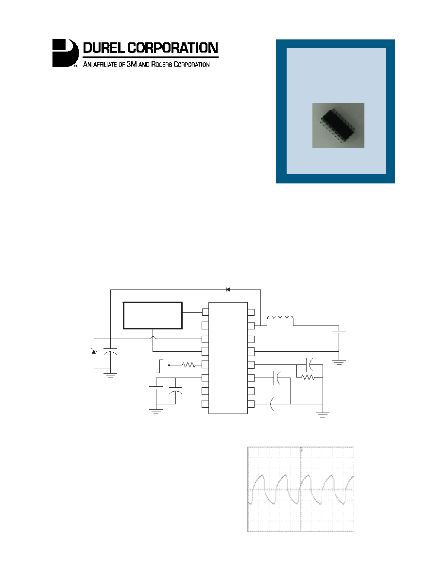
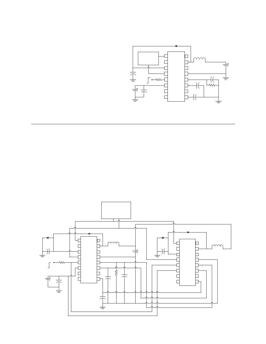
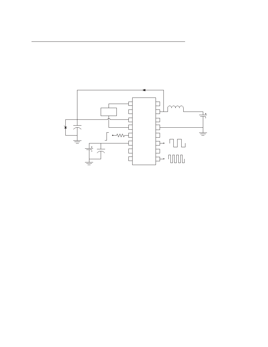
Sample Application Circuit
Data Sheet
D306A
Electroluminescent
Lamp Driver IC
D306A
SOIC - 16 with Heat Slug
Typical Output
Brightness = 24.5 fL (83.9 cd/m
2
)
Lamp Frequency = 448 Hz
Logic Supply Current = 25 mA
Power Supply Current = 42 mA
Vout = 330 Vpp
Load = 6 in
2
(38.7 cm
2
) Durel
Æ
Green EL
BAS21
2.2nF
(200V)
0
ON
OFF
3.3mH Coilcraft
D03316
220pF
10nF
100pF
100k
Vbat = 12.0V
1
2
3
4
5
6
7
8
CLF
CHF
Rf
Cs
Va
Vb
Vcc
NC
E
L
NC
GND
NC
NC
NC
NC
16
15
14
13
12
11
10
9
5.0V
200V
D306A
EL Lamp
+
-
+
-
Sample Output Waveform
2
Absolute Maximum Ratings
*At a given ambient temperature, the maximum power rating can be calculated with the following equation: T
j
= P(
ja
)+T
a
.
Note: The above are stress ratings only. Functional operation of the device at these ratings or any other above those indicated in the
specifications is not implied. Exposure to absolute maximum rating conditions for extended periods of time may affect reliability.
Parameter
Symbol
Minimum
Maximum
Unit
Comments
Supply Voltage
Operating Range
Vbat
2.0
12
V
E = Vcc
Withstand Range
-0.5
16
E = GND
Logic Drive Voltage
Operating Range
Vcc
2
5
V
E = Vcc
Withstand Range
-0.5
6
E = GND
Enable Voltage
E
-0.5
Vcc + 0.5
V
Vout
Va - Vb
410
Vpp
E = Vcc
Operating Temperature
T
a
*
-40
85
∞C
Ambient
T
j
125
∞C
Junction
Average Thermal Resistance
ja
40
∞C/W
Junction to Ambient
Storage Temperature
T
s
-55
150
∞C
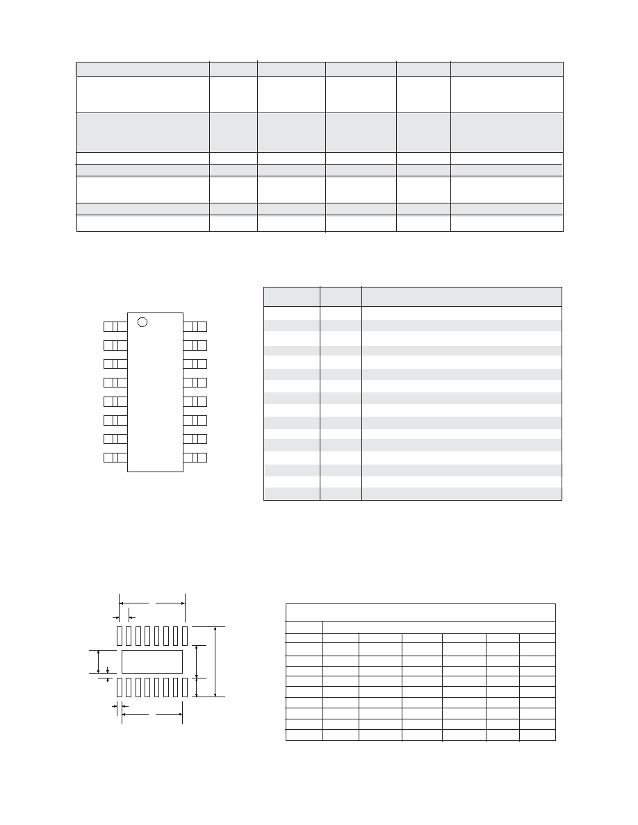
Physical Data
1
2
3
4
5
6
7
8
16
15
14
13
12
11
10
9
PIN # NAME
FUNCTION
1
Va
AC voltage output to EL lamp
2
NC
No connect
3
Cs
High voltage storage capacitor to input
4
Vb
AC voltage output to EL lamp
5
E
System enable: Wave-shaping resistor control
6
Vcc
Logic drive voltage
7
NC
No connect
8
NC
No connect
9
CHF
Capacitor input to high frequency oscillator
10
NC
No connect
11
CLF
Capacitor input to low frequency oscillator
12
Rf
Resistor input for frequency control
13
GND
Power ground
14
NC
No connect
15
L
Inductor input
16
NC
No connect
RECOMMENDED PAD LAYOUT
a
b
c
d
e
f
g
h
i
a
1.270
0.050
b
8.890
0.350
c
4.267
0.168
4.673
0.184
d
0.609
0.024
0.711
0.028
0.812
0.032
e
5.791
0.228
6.197
0.244
f
0.545
0.021
g
8.748
0.344
h
0.830
0.033
i
3.437
0.135
mm.
in.
mm.
in.
mm.
in.
Min.
Typical
Max.
SOIC-16 with Heat Slug PAD LAYOUT
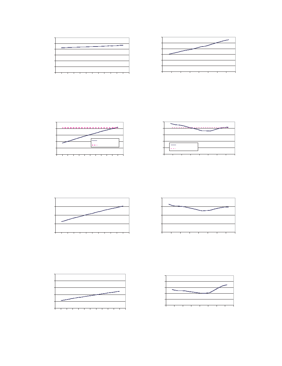
3
Typical Performance Characteristics Using Standard Test Circuit
Output Frequency vs. DC Supply Voltage
Output Frequency vs. Ambient Temperature
Output Voltage (Vpp) vs. DC Supply Voltage
Output Voltage (Vpp) vs. Ambient Temperature
Supply Current (Ibat) vs. DC Supply Voltage
Supply Current (Ibat) vs. Ambient Temperature
Output Voltage (Vrms) vs. DC Supply Voltage
Output Voltage (Vrms) vs. Ambient Temperature
0
100
200
300
400
500
600
5
6
7
8
9
10
11
12
13
14
15
16
17
DC Input Voltage (Vbat)
LF (Hz)
0
100
200
300
400
500
5
6
7
8
9 10 11 12 13 14 15 16 17
DC Input Voltage (Vbat)
Output V
olta
g
e
(Vpp)
Output Voltage
Vout Max
0
50
100
150
200
5
6
7
8
9
10
11
12
13
14
15
16
17
DC Input Voltage (Vbat)
Output V
olta
g
e
(Vrms)
0
20
40
60
80
100
5
6
7
8
9
10 11 12 13 14 15 16 17
DC Input Voltage (Vbat)
A
vg Suppl
y Current (mA)
0
100
200
300
400
500
600
-60
-40
-20
0
20
40
60
80
100
Temperature (
o
C)
LF (Hz)
0
100
200
300
400
500
-60
-40
-20
0
20
40
60
80
100
Temperature (
o
C)
Output V
olta
g
e
(Vpp)
Output Voltage
Vout Max
0
50
100
150
200
-60
-40
-20
0
20
40
60
80
100
Temperature (
o
C)
Output V
olta
g
e
(Vrms)
0
20
40
60
80
100
-60
-40
-20
0
20
40
60
80
100
Temperature (
o
C)
A
vg Suppl
y Current (mA)
4
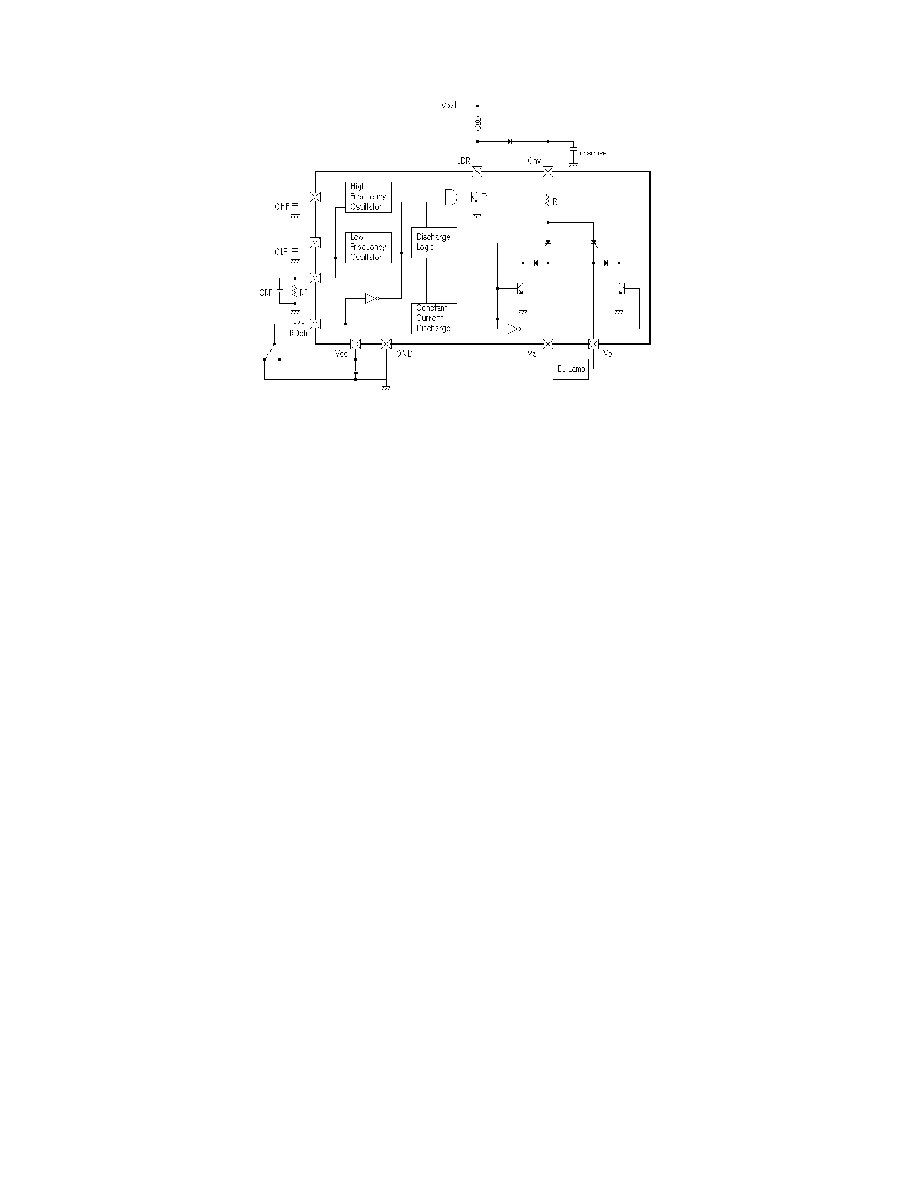
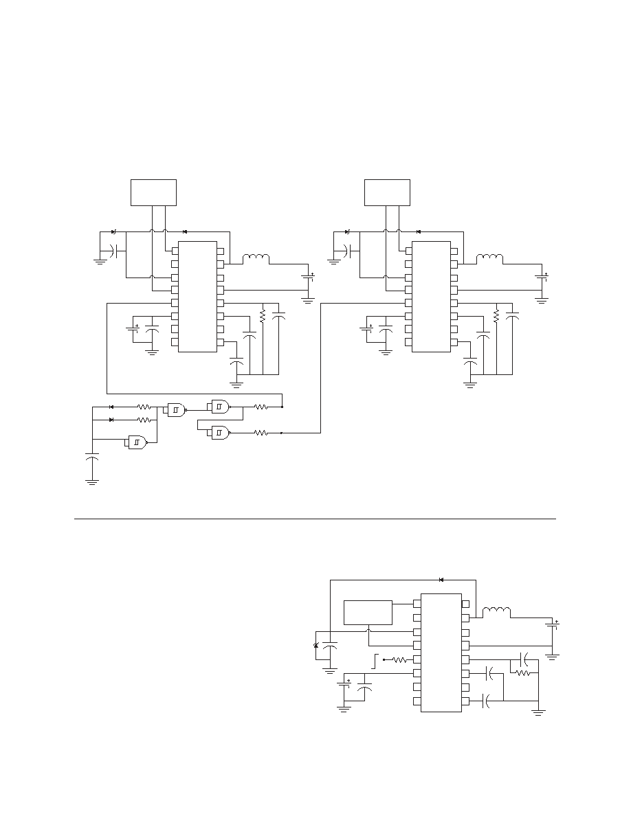
Theory of Operation
Electroluminescent (EL) lamps are essentially capacitors with one transparent electrode and a special phosphor
material in the dielectric. When a strong AC voltage is applied across the EL lamp electrodes, the phosphor
glows. The required AC voltage is typically not present in most systems and must be generated from a low
voltage DC source.
The D306A IC inverter drives the EL lamp by using a switching transistor to repeatedly charge an external
inductor and discharge it to the high voltage capacitor Cs. The discharging causes the voltage at Cs to
continually increase. The internal circuitry uses the H-bridge technology, using both electrodes to drive the
EL lamp. One of the outputs, Va or Vb, is used to discharge Cs into the EL lamp during the first half of the
low frequency (LF) cycle. By alternating the state of the H-bridge, the other output is used to charge the EL
lamp during the second half of the LF cycle. The alternating states make it possible to achieve 400V peak-
to-peak across the EL lamp.
The EL driving system is divided into several parts: on-chip logic control, on-chip high voltage output
circuitry, on-chip discharge logic circuitry, and off-chip components. The on-chip logic controls the lamp
operating frequency (LF) and the inductor switching frequency (HF). These signals are used to drive the
high voltage output circuitry (H-bridge) by delivering the power from the inductor to the lamp. The integrated
discharge logic circuitry uses a patented wave shaping technique for reducing audible noise from an EL
lamp. Changing the Rd value changes the slope of the linear discharge as well as the shape of the waveform.
The off-chip component selection provides a degree of flexibility to accommodate various lamp sizes, system
voltages, and brightness levels.
Typical D306A EL driving configurations for driving EL lamps in various applications are shown on the
following page. The expected system outputs for the various circuit configurations are also shown with each
respective figure. These examples are only guides for configuring the driver. Durel provides a D306A
Designer's Kit, which includes a printed circuit evaluation board intended to aid you in developing an EL
lamp driver configuration using the D306A that meets your requirements. A section on designing with the
D306A is included in this datasheet to serve as a guide to help you select the appropriate external components
to complete your D306A EL driver system.
Block Diagram of the Driver Circuitry
5
Typical D306A EL Driver Configurations
12.0 V Dual D306A for Sign Backlight
Typical Output
Brightness = 27.1 fL (92.8 cd/m
2
)
Lamp Frequency = 525 Hz
Logic Supply Current = 48 mA
Power Supply Current = 212 mA
Vout = 368 Vpp
Load = 18.3 in
2
(118 cm
2
) Durel
Æ
White EL
BAS21
2.2nF
(200V)
10 kOhm
ON
OFF
470uH
TDK SLF7032
68pF
8.2nF
100pF
100kOhm
5.0V
1
2
3
4
5
6
7
8
CLF
CHF
Rf
Cs
Va
Vb
Vcc
NC
E
L
NC
GND
NC
NC
NC
NC
16
15
14
13
12
11
10
9
5.0V
D306A
PDA LCD
EL Lamp
5.0V PDA Display
Typical Output
Brightness = 22.0 fL (75.4 cd/m
2
)
Lamp Frequency = 370 Hz
Logic Supply Current = 25 mA
Power Supply Current = 108 mA
Vout = 380 Vpp
Load = 5 in
2
(32.2 cm
2
) Durel
Æ
Green EL
White
EL Lamp
BAS21
2.2nF
(200V)
10 kOhm
ON
OFF
1.5mH
Coilcraft D03316P
220pF
6.8nF
100pF
100kOhm
12.0V
1
2
3
4
5
6
7
8
16
15
14
13
12
11
10
9
Va
NC
Cs
Vb
E
Vcc
NC
NC
NC
L
NC
NC
GND
Rf
CLF
CHF
1.5mH
Coilcraft D03316P
2.2nF
(200V)
BAS21
1
2
3
4
5
6
7
8
CLF
CHF
Rf
Cs
Va
Vb
Vcc
NC
E
L
NC
GND
NC
NC
NC
NC
16
15
14
13
12
11
10
9
5.0V
200V
200V
D306A
D306A
6
3.6V Alternating Circuit*
Typical Output EL Lamp 1
Brightness = 14 fL (48.0 cd/m
2
)
Lamp Frequency = 300 Hz
Logic Supply Current = 24 mA
Power Supply Current = 74 mA
Vout = 272 Vpp
Load = 8 in
2
(cm
2
) Durel
Æ
White EL
Typical Output EL Lamp 2
Brightness = 14 fL (48.0 cd/m
2
)
Lamp Frequency = 300 Hz
Logic Supply Current = 24 mA
Power Supply Current = 74 mA
Vout = 272 Vpp
Load = 8 in
2
(cm
2
) Durel
Æ
White EL
9.0V Large Signage Lamp
Typical Output
Brightness = 4.90 fL (16.8 cd/m
2
)
Lamp Frequency = 335 Hz
Logic Supply Current = 24 mA
Power Supply Current = 148 mA
Vout = 224 Vpp
Load = 30 in
2
(193.5 cm
2
) Durel
Æ
Green EL
BAS21
2.2nF
(200V)
10 kOhm
ON
OFF
1.0mH
Coilcraft D03316
68pF
10nF
100pF
100kOhm
12.0V
1
2
3
4
5
6
7
8
CLF
CHF
Rf
Cs
Va
Vb
Vcc
NC
E
L
NC
GND
NC
NC
NC
NC
16
15
14
13
12
11
10
9
Large Area
EL Lamp
5.0V
200V
D306A
*Note: Two separate backlight systems are alternately enabled using the same supply lines.
1N4148
1N4148
10kohm
10kohm
100kohm
100kohm
2.2uF
E1
E2
8in
2
EL Lamp 1
BAS21
10nF
(200V)
.680mH
Coilcraft D03316P
220pF
6.8nF
100pF
100kOhm
3.6V
1
2
3
4
5
6
7
8
CLF
CHF
Rf
Cs
Va
Vb
Vcc
NC
E
L
NC
GND
NC
NC
NC
NC
16
15
14
13
12
11
10
9
3.0V
200V
D306A
8in
2
EL Lamp 2
BAS21
10nF
(200V)
.680mH
Coilcraft D03316P
220pF
6.8nF
100pF
100kOhm
3.6V
1
2
3
4
5
6
7
8
CLF
CHF
Rf
Cs
Va
Vb
Vcc
NC
E
L
NC
GND
NC
NC
NC
NC
16
15
14
13
12
11
10
9
3.0V
200V
D306A
CD4011 or equivalent
7
Designing With D306A
There are many variables which can be optimized to
achieve the desired performance for specific
applications. The luminance of the EL lamp is a
function of the output voltage applied to the lamp by
the IC, the frequency at which the voltage is applied,
the lamp material properties, and the lamp size. Durel
offers the following component selection aids to help
the designer select the optimum circuit configuration.
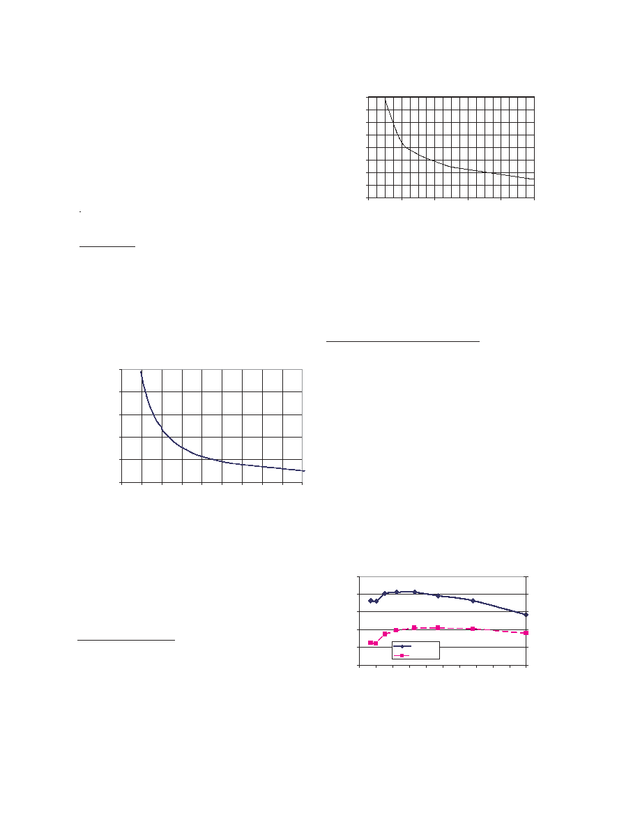
I. Lamp Frequency Capacitor (CLF)
Selection
Selecting the appropriate value of capacitor (CLF)
for the low frequency oscillator will set the output
frequency of the D306A EL driver IC. Figure 1
graphically represents the effect of the CLF capacitor
value on the oscillator frequency at Vbat = 13.5V,
Vcc = 5.0V.
Figure 1: Typical Lamp Frequency vs. CLF Capacitor
Figure 2: Typical Inductor Frequency vs.CHF Capacitor
II. Inductor Switching Frequency
(CHF) Selection
Selecting the appropriate value of capacitor (CHF)
for the high frequency oscillator will set the inductor
switching frequency of the D306A inverter. Figure 2
graphically represents the effect of the CHF capacitor
value on the oscillator frequency at Vbat = 13.5V,
Vcc = 5.0V.
0
0
10
10
20
20
30
30
40
40
50
50
60
60
70
70
80
80
0
0
200
200
400
400
600
600
800
800
1000
1000
CHF (pF)
CHF (pF)
Inductor Frequency (kHz)
Figure 3: Brightness and current vs. inductor value
Conditions:
Vcc = 5V, Vbat = 6.5V, 6.1 in
2
(39.4 cm
2
) EL Lamp
III. Inductor (L) Selection
The inductor value has a large impact on the output
brightness and current consumption of the driver.
Figure 3 shows typical brightness and current draw
of a D306A circuit with different inductor values.
Please note that the DC resistance (DCR) and current
rating of inductors with the same inductance value
may vary with manufacturer and inductor type. Thus,
inductors made by a different manufacturer may yield
different outputs, but the trend of the different curves
should be similar. This curve is intended to give the
designer a relative scale from which to optimize
specific applications. Absolute measurements may
vary depending upon the type and brand of other
external components selected.
0
5
10
15
20
25
0
1
2
3
4
5
6
7
8
9
10
Inductor Value (mH)
Luminance (fL)
60
80
100
120
140
160
Current Dra
w (mA)
Luminance
Current
0
200
400
600
800
1000
0
5
10
15
20
25
30
35
40
45
CLF (nF)
Lamp Frequenc
y (Hz)

8
VI. Rf and CRf Selection
The combination of Rf and timing capacitors, CLF
and CHF, determines the time constants for the low
frequency oscillator and the high frequency oscillator,
respectively. To simplify the tuning of the oscillator
frequencies to the desired frequency range, a standard
value is recommended for Rf = 100 k
.
The CRf capacitor is used as a stabilizing capacitor
to filter noise on the Rf line. A small 100pF capacitor
is typical and sufficient value for CRf.
VII. Fast Recovery Diode
Energy stored by the coil is eventually forced through
the external diode to power the switched H-bridge
network. A fast recovery diode, such as BAS21, is
recommended for this function for optimum
operation.
VIII. Printed Circuit Board Layout
The high frequency operation and very high voltage
IV. Wave-Shape Selection
The D306A EL Driver uses a patented wave-shaping
technique for reducing audible noise from an EL lamp.
The slope of the discharge section of the output
waveform may be adjusted by selecting a proper value
for the wave-shape discharge resistor (Rd) in series
with the E pin input. The optimal discharge level for
an application depends on the lamp size, lamp
brightness, and application conditions. To ensure that
the D306A is configured optimally, various discharge
levels should be evaluated. In many cases, lower
discharge levels may result in lower audible noise
from the EL lamp. The recommended typical value
for Rd is 10 k
.
V. Storage Capacitor (Cs) Selection
The Cs capacitor is used to store the energy transferred
from the inductor before discharging the energy to
the EL lamp. Cs values can range from 1.5nF to 4.7nF
and must have minimum 200V rating. In general, the
Cs value does not have a large affect on the output of
the device. The typical Cs capacitor recommendation
is 2.2nF with 200V rating.
output of the D306A makes printed circuit board
layout important for minimizing electrical noise.
Maintain the IC connections to the inductor as short
as possible. Connect the GND of the device directly
to the GND plane of the PCB. Keep the GND pin of
the device and the ground leads of the Cs, CLF, and
CHF less than 5mm apart. If using bypass capacitors
to minimize ripple on the supply lines, keep the
bypass caps as close as possible to the Vbat lead of
the inductor and the Vcc pin.
The higher than normal operating temperature of the
D306A also requires additional ground heat planes
on the printed circuit board layout. The D306A has a
heat slug attached to the bottom of the packge to
provide additional heat dissipation. It is recommended
that the PCB incorporate a complimentary grounded
heat plane to solder connect to the heat slug of the
package. It is also recommended that no electrical
traces, which can be adversely affected by the
temperature transfer and the high voltage output, be
laid out underneath the device. The temperture
transfer, as well as high voltage output, may adversely
affect these electrical traces. Recommended pad
layout dimensions can be found on the last page of
this datasheet.
IX. Optional Zener Diodes
The D306A EL driver circuit should be designed such
that the output voltage of the device does not exceed
the maximum rated value of 400Vpp. Operating the
D306A above this rating can cause irreversible
damage to the device. This condition is most likely
in applications, such as in automotive instrument
clusters, where the supply voltage (Vbat) is higher
than 6.0V and can generate output voltage greater
than 400Vpp. Extreme temperature change can also
cause the output voltage to exceed the maximum
rating, especially when the nominal operating voltage
of the device is close to the maximum limit at room
temperature.
A zener diode connected in parallel to the Cs capacitor
and ground of the D306A is recommended to limit
the device output to less than 400Vpp. This
component is optional and may be avoided in
applications which are known to function only within
safe operating conditions.
9
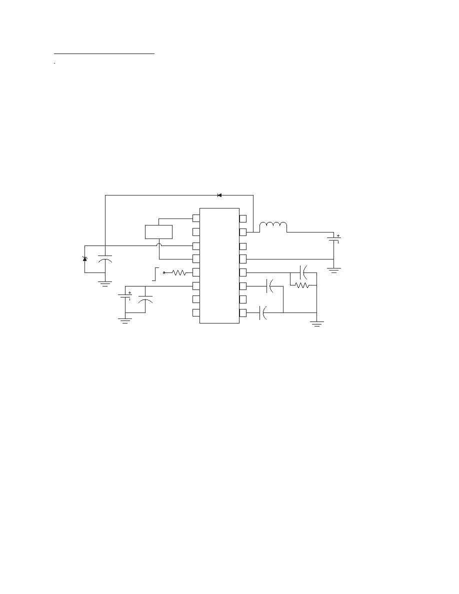
X. Split Voltage Supply
A split supply voltage is recommended to drive the
D306A. To operate the on-chip logic, a regulated
voltage supply (Vcc) ranging from 2.0V to 6.5V is
applied. To supply the D306A with the necessary
power to drive an EL lamp, another supply voltage
(Vbat) with higher current capability is applied to
the inductor. The voltage range of Vbat is determined
by the following conditions: user application, lamp
size, inductor selection, and power limitations of the
battery.
An example of the split supply configuration is shown
below. This example shows a regulated 5.0V applied
to the Vcc pin, and a Vbat voltage that may range
from 9.0V to 16.0V or regulated at 13.5V. The enable
voltage is in the range of 3.0V to 5.0V. This is a typical
setup used in automotive applications.
BAS21
2.2nF
(200V)
0 Ohm
ON
OFF
6.8mH
Coilcraft D03316
120pF
10nF
100pF
100kOhm
9.0V - 16.0V Battery
or 13.5V Regulated
1
2
3
4
5
6
7
8
CLF
CHF
Rf
Cs
Va
Vb
Vcc
NC
E
L
NC
GND
NC
NC
NC
NC
16
15
14
13
12
11
10
9
Automotive
EL Lamp
5.0V
200V
D306A
10
D306A Design Ideas
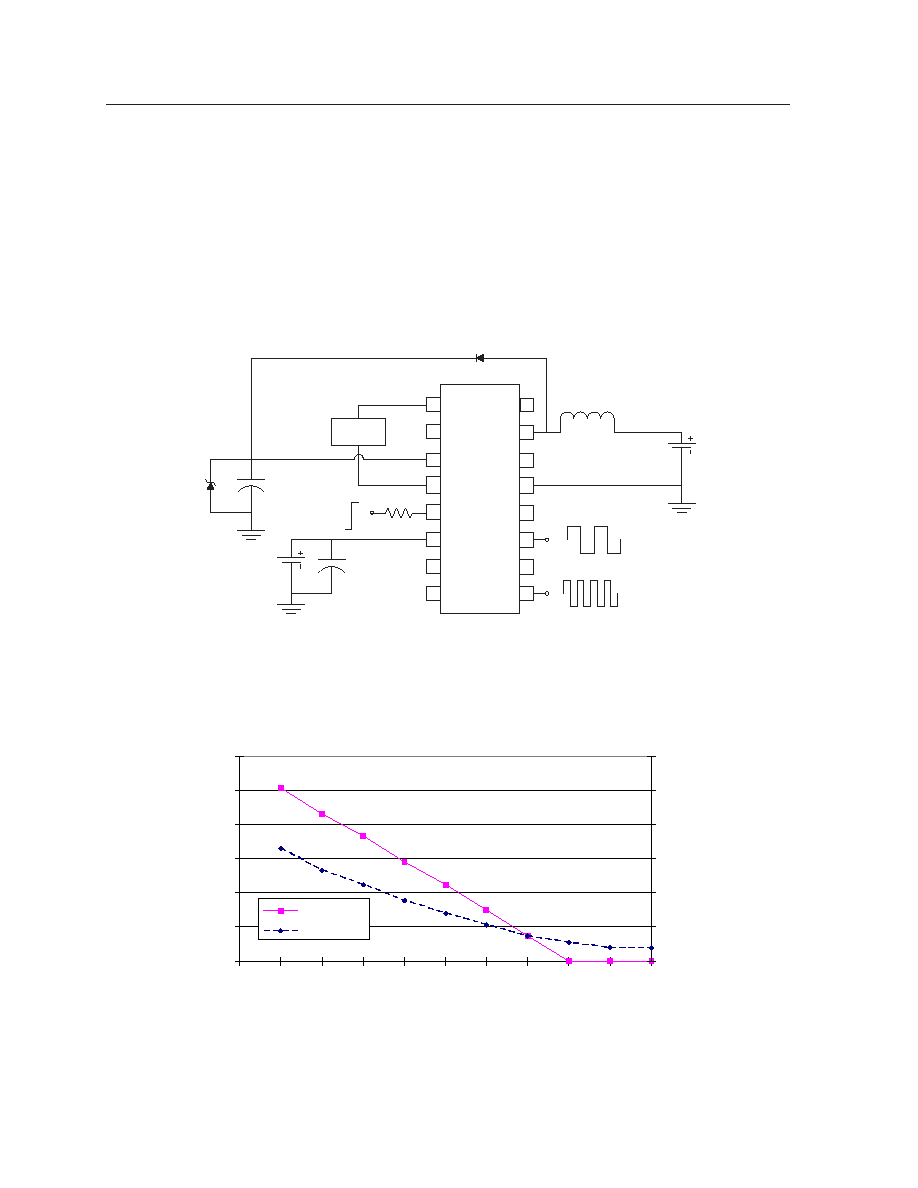
I. Controlling Output Frequency Using External Clock Signals
External clock signals may be used to control the D306A oscillator frequencies instead of adding external
passive components. When clocking signals provide both the inductor charging (HF) and lamp output (LF)
oscillator frequencies to drive the D306A, the CLF, CHF, Rf, and CRf components are no longer required. A
sample configuration demonstrating this cost-saving option is shown below.
In this configuration, the lamp frequency is controlled by the signal applied to the CLF pin. An internal
divider network in the IC divides the frequency of the LF input signal by two. Thus, to get a 400 Hz AC
output waveform to drive the EL lamp, an 800 Hz square-wave input signal should be connected to the CLF
pin. Input clocking frequencies may range from 400 Hz to 2000 Hz, with 10-20% positive duty cycle for
optimum brightness. The amplitude of the clock signal typically ranges from 1.0V to Vcc.
The high frequency oscillator that determines inductor charging frequency is controlled above by a digital
AC signal into the CHF pin. The HF clock signal frequency may range from 20KHz - 35KHz, with 10-20%
positive duty cycle for optimum lamp intensity. The amplitude of the clock signal typically ranges from
1.0V to Vcc.
BAS21
2.2nF
(200V)
10 kOhm
ON
OFF
6.5V
1
2
3
4
5
6
7
8
CLF
CHF
Rf
Cs
Va
Vb
Vcc
NC
E
L
NC
GND
NC
NC
NC
NC
16
15
14
13
12
11
10
9
EL Lamp
5.0V
200V
800 Hz
15% + duty
1.0V Min
0.2V Max
32 kHz
10% + duty
1.0V Min
0.2V Max
D306A
11
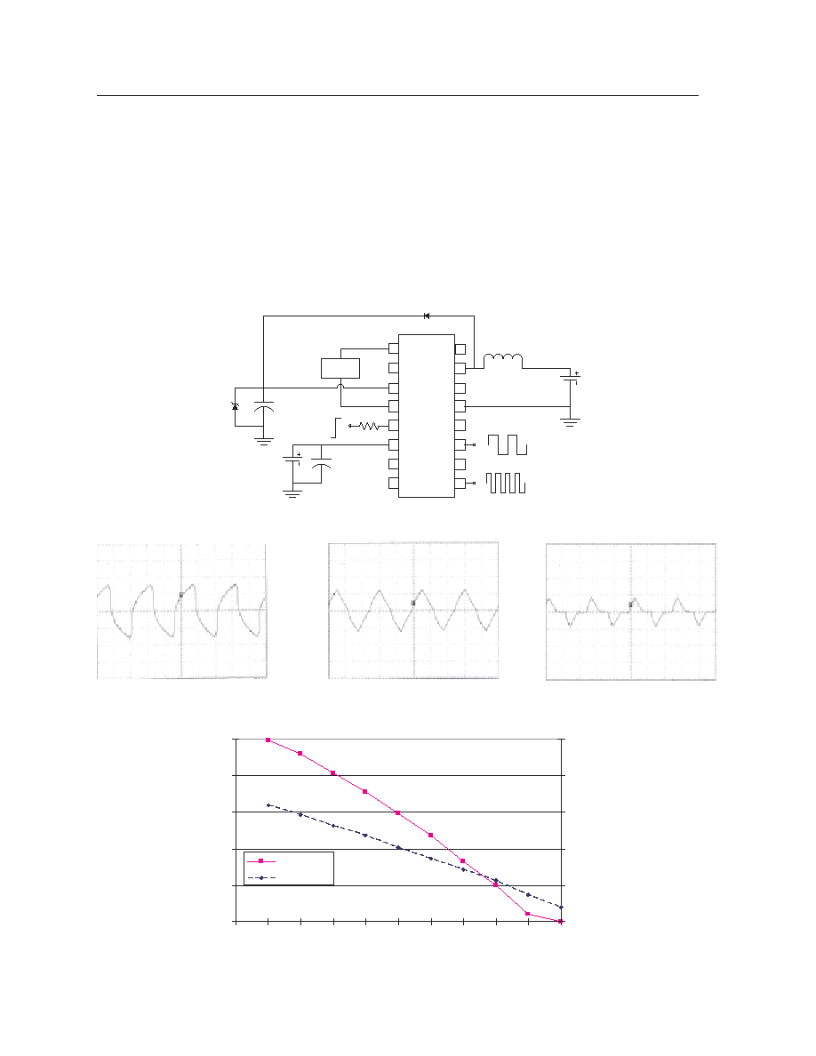
II. Controlling EL Brightness through Clock Pulse Width Modulation (Option 1)
Pulse width modulation of the external LF input signal may be used to regulate the brightness of the EL
lamp. Figures 4, 5, and 6 below demonstrate examples of the D306A output waveform with pulse width
modulation of the LF input signal. As the positive duty cycle of the LF input signal is increased from 10% to
100%, the charging period of the output waveform decreases, and the peak voltage of the output waveform
also decreases towards zero output. Therefore, incremental dimming occurs as a result of the wave-shaping
changes. This scheme may also be used inversely to regulate lamp brightness over the life of the battery or
to compensate for lamp aging. Figure 7 shows a typical dimming curve with this technique. Operation at
duty cycles lower than 10% is not recommended. Clocking frequency can range from 400 Hz to 2000 Hz.
The maximum amplitude of the clock signal may range from 1.0V to Vcc.
Figure 4: LF Input Duty Cycle = +10%
Figure 5: LF Input Duty Cycle = +50%
Figure 6: LF Input Duty Cycle = +75%
Figure 7: Dimming through LF Clock Input Duty Cyle
BAS21
2.2nF
(200V)
10 kOhm
ON
OFF
6.5V
1
2
3
4
5
6
7
8
CLF
CHF
Rf
Cs
Va
Vb
Vcc
NC
E
L
NC
GND
NC
NC
NC
NC
16
15
14
13
12
11
10
9
EL Lamp
5.0V
200V
800 Hz
10% to 100%
positive duty PWM
1.0V Min
0.2V Max
32 kHz
10% positive duty
1.0V Min
0.2V Max
D306A
0
4
8
12
16
20
0%
10%
20%
30%
40%
50%
60%
70%
80%
90% 100%
LF Clock Input Duty Cycle
Luminance (fL)
0
30
60
90
120
150
Current Dra
w (mA)
Luminance
Current
12
III. Controlling EL Brightness through Clock Pulse Width Modulation (Option 2)
Pulse width modulation of the external HF input signal also may be used to regulate the brightness of the EL
lamp. As the positive duty cycle of the HF input signal is increased from 10% to 80%, the peak voltage of the
output waveform decrease incrementally to zero output as the inductor charging period is affected by the HF
duty cycle. Lamp dimming is thus achieved with pulse width modulation of the HF input signal to the
D306A. This scheme may also be used inversely to regulate lamp brightness over the life of the battery or to
compensate for lamp aging. Figure 8 shows a typical dimming curve with this technique. The recommended
HF duty cycle range is from 10% to 80%. Clocking frequency can range from 20 KHz to 35 KHz. The
maximum amplitude of the clock signal may range from 1.0V to Vcc.
Figure 8: Dimming through HF Clock Input Duty Cyle
0
4
8
12
16
20
24
0%
10% 20% 30% 40% 50% 60% 70% 80% 90% 100%
CHF Clock Input Duty Cycle
Lum
i
n
anc
e
(
f
L
)
0
30
60
90
120
150
180
C
u
r
r
en
t
D
r
aw
(
m
A
)
Luminance
Current
BAS21
2.2nF
(200V)
10 kOhm
ON
OFF
6.5V
1
2
3
4
5
6
7
8
CLF
CHF
Rf
Cs
Va
Vb
Vcc
NC
E
L
NC
GND
NC
NC
NC
NC
16
15
14
13
12
11
10
9
EL Lamp
5.0V
200V
800 Hz
10% positive Duty
1.0V Min
0.2V Max
32 kHz
10% to 80%
positive duty PWM
1.0V Min
0.2V Max
D306A
13
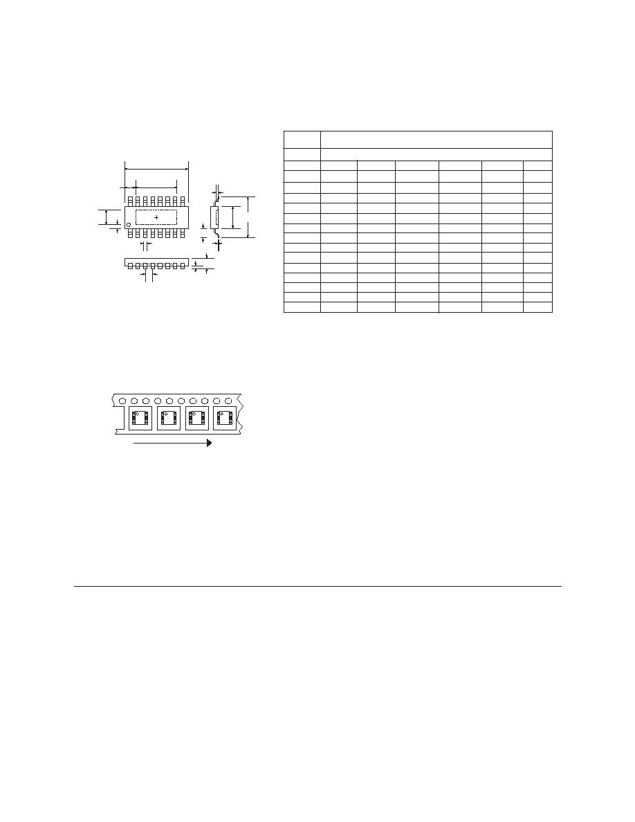
The D306A IC is available in standard SOIC-16 narrow body with heat slug plastic package per tape and
reel. A Durel D306A Designer's Kit (1DDD306AA-K01) provides a vehicle for evaluating and identifying
the optimum component values for any particular application using D306A. Durel engineers also provide
full support to customers including specialized circuit optimization and application retrofits upon request.
Ordering Information:
DUREL Corporation
2225 W. Chandler Blvd.
Chandler, AZ 85224-6155
Tel: (480) 917-6000
FAX: (480) 917-6049
Website: http://www.durel.com
© 2002, 2003 Durel Corporation
Printed in U.S.A.
LIT-I 9047 Rev. A03
The DUREL name and logo are registered trademarks of DUREL CORPORATION. Wave-shaping is a trademark of Durel Corporation.
This information is not intended to and does not create any warranties, express or implied, including any warranty of merchantability or fitness
for a particular purpose. The relative merits of materials for a specific application should be determined by your evaluation.
This driver IC is covered by the following U.S. patents: #5,313,141, #5,789,870, #6,297,597 B1. Corresponding foreign patents are issued and
pending.
ISO 9001 Certified
A
B
C
D
E
F
G
H
I
N
K
J
L
M
A
1.372
0.052
1.550
0.061
1.727
0.068
B
0.102
0.004
0.176
0.007
0.249
0.010
C
0.330
0.013
0.419
0.017
0.508
0.020
D
0.864
0.034
1.042
0.041
1.219
0.048
E
0.191
0.008
0.220
0.009
0.249
0.010
F
9.802
0.386
9.901
0.390
9.999
0.394
G
1.016
0.040
1.270
0.050
1.524
0.060
H
5.791
0.228
5.994
0.236
6.197
0.244
I
3.861
0.152
3.925
0.115
3.988
0.157
J
2.794
0.110
K
0.566
0.022
L
1.395
0.055
M
7.112
0.280
N
0.432
0.017
Description
mm.
in.
mm.
in.
mm.
in.
SOIC-16 with Heat Slug
Min.
Typical
Max.
SOICs in Tape and Reel: 1DDD306AA-S06
Embossed tape on 360 mm diameter reel 2500 units per
reel. Quantity marked on reel label.
Tape Orientation
SOIC's are marked with part number (306A) and
3-digit wafer lot code. Bottom of marking is on
the Pin 1 side.