 | –≠–ª–µ–∫—Ç—Ä–æ–Ω–Ω—ã–π –∫–æ–º–ø–æ–Ω–µ–Ω—Ç: D365A | –°–∫–∞—á–∞—Ç—å:  PDF PDF  ZIP ZIP |
1
(Using Standard Test Circuit at Ta=25∞C, unless otherwise specified)
Lamp Driver Specifications
Lamp Driver Specifications
Lamp Driver Specifications
Lamp Driver Specifications
Lamp Driver Specifications
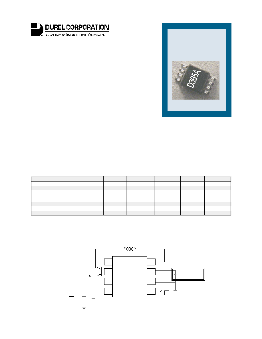
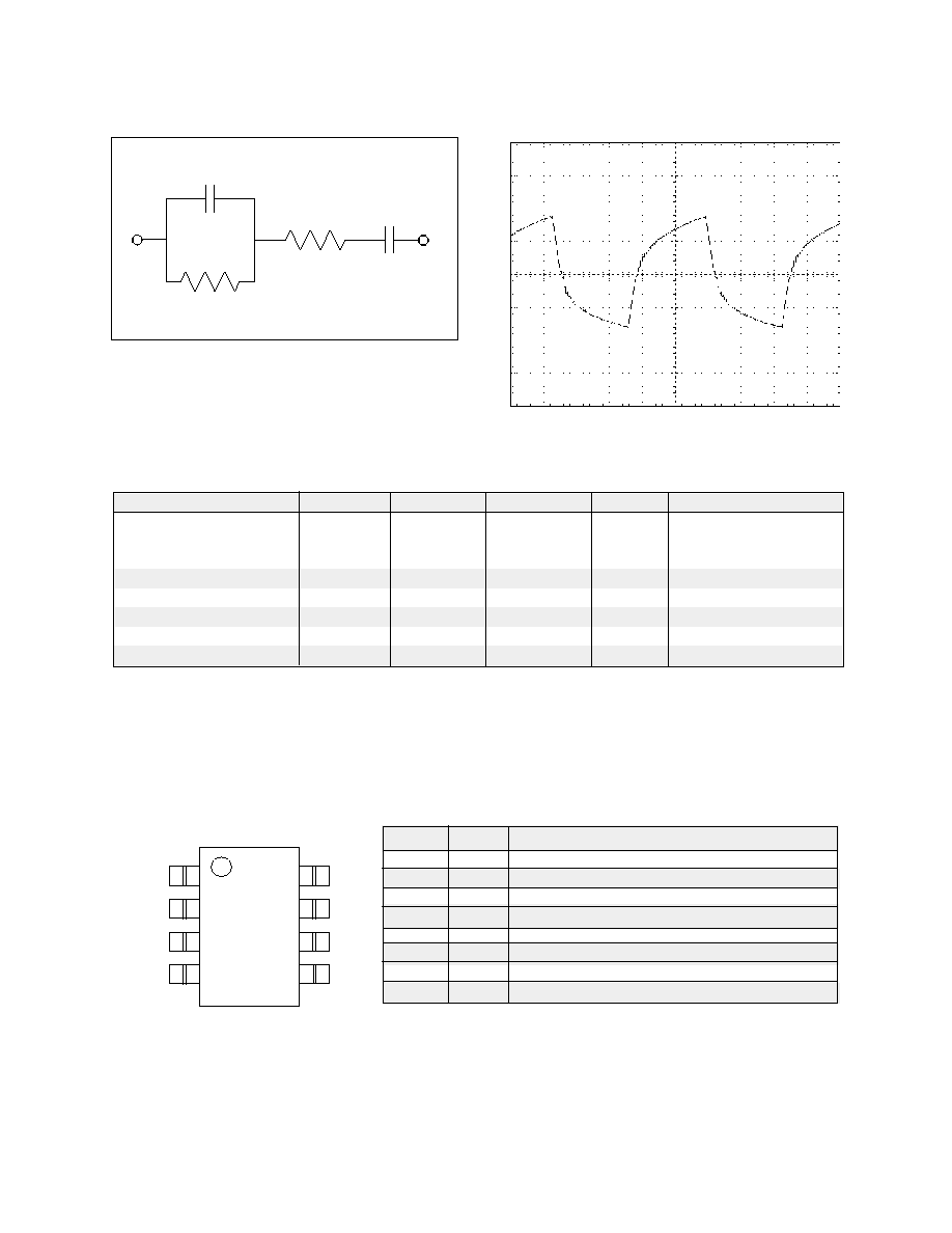
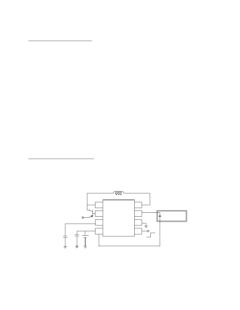
Standard Test Circuit
Standard Test Circuit
Standard Test Circuit
Standard Test Circuit
Standard Test Circuit
General Description
General Description
General Description
General Description
General Description
The DurelÆ D365 is part of a family of highly integrated EL drivers
based on Durel's patented three-port (3P) topology which offers
built-in EMI shielding. The D365 IC and three components make a
complete EL lamp driving circuit. Equipped with a patented
discharge circuitry, the D365 device offers low-noise performance
in applications that are sensitive to audible and electrical noise.
Data Sheet
Data Sheet
Data Sheet
Data Sheet
Data Sheet
D365A
D365A
D365A
D365A
D365A
Electroluminescent
Electroluminescent
Electroluminescent
Electroluminescent
Electroluminescent
Lamp Driver IC
Lamp Driver IC
Lamp Driver IC
Lamp Driver IC
Lamp Driver IC
MSOP-8
MSOP-8
MSOP-8
MSOP-8
MSOP-8
Features
Applications
!
!
!
!
!
Integrated Low Noise Circuitry
!
!
!
!
!
Cellular Phones and Handsets
!
!
!
!
!
High AC Voltage Output
!
!
!
!
!
Data Organizers/PDAs
!
!
!
!
!
Circuit Topology Shields EMI
!
!
!
!
!
LCD Backlighting
!
!
!
!
!
Drives up to 20 in
2
EL Lamps
!
!
!
!
!
Small Package Size
1
2
3
4
8
7
6
5
L+
VOUT
V+
GND
L-
CHF
E
1mH
DCR = 2
D365
3.3 V
BASE
Load "B"
6.8 nF
0.1
µ
F
MPSA56
pnp
3.3 V
OFF
ON
Parameter
Parameter
Parameter
Parameter
Parameter
Symbol
Symbol
Symbol
Symbol
Symbol
Minimum
Minimum
Minimum
Minimum
Minimum
Typical
Typical
Typical
Typical
Typical
Maximum
Maximum
Maximum
Maximum
Maximum
Unit
Unit
Unit
Unit
Unit
Conditions
Conditions
Conditions
Conditions
Conditions
nA
E = GND
mA
E = V+
µA
E = V+
nA
E = GND
Vpp
E = V+
Hz
E = V+
kHz
E = V+
Standby Current
40
1000
Supply Current
I
44
60
Enable Current
ON
15
50
OFF
20
Output Voltage
Vout
160
175
280
Lamp Frequency
LF
236
267
330
Inductor Oscillator frequency
HF
17
19.2
24
2
Supply Voltage
Operating Range
V+
2.5
6.5
V
E=V+
Withstand Range
-0.5
7.0
E=GND
Enable Voltage
E
-0.5
(V+) +0.5
V
Lamp Output
Vpeak
140
V
Positive peak voltage
Power Dissipation
Pd
250
mW
Operating Temperature
T
a
-20
85
∞C
Storage Temperature
T
s
-40
150
∞C
Absolute Maximum Ratings
Absolute Maximum Ratings
Absolute Maximum Ratings
Absolute Maximum Ratings
Absolute Maximum Ratings
Physical Data
Physical Data
Physical Data
Physical Data
Physical Data
Note: The above are stress ratings only. Functional operation of the device at these ratings or any other above those indicated in the specification is not
implied. Exposure to absolute maximum rating conditions for extended periods of time may affect reliability.
100
22 nF
10k
47 nF
* Load B approximates a 5in
2
EL lamp.
Parameter
Parameter
Parameter
Parameter
Parameter
Symbol
Symbol
Symbol
Symbol
Symbol
Minimum
Minimum
Minimum
Minimum
Minimum
Maximum
Maximum
Maximum
Maximum
Maximum
Unit
Unit
Unit
Unit
Unit
Comments
Comments
Comments
Comments
Comments
Pin #
Pin #
Pin #
Pin #
Pin # Name
Name
Name
Name
Name
Function
Function
Function
Function
Function
1
L+
Positive input to inductor
2
B a s e
PNP transistor base connection
3
CHF
High frequency oscillator capacitor/clock input
4
V+
DC power supply input
5
E
System enable; HI=On
6
GND
System ground connection
7
Vout
AC output to lamp
8
L-
Negative input to inductor
Load B*
Load B*
Load B*
Load B*
Load B*
Typical Output Waveform
Typical Output Waveform
Typical Output Waveform
Typical Output Waveform
Typical Output Waveform
1
2
3
4
5
6
7
8

3
Output Frequency vs. Ambient
Temperature
0
50
100
150
200
250
300
350
400
-20
0
20
40
60
80
Temperature ( C)
LF (Hz)
Typical Performance Characteristics Using Standard Test Circuit
Typical Performance Characteristics Using Standard Test Circuit
Typical Performance Characteristics Using Standard Test Circuit
Typical Performance Characteristics Using Standard Test Circuit
Typical Performance Characteristics Using Standard Test Circuit
∞∞
∞∞
∞
∞∞
∞∞
∞
∞∞
∞∞
∞
Output Frequency vs. DC Supply
Voltage
0
50
100
150
200
250
300
350
400
2
3
4
5
6
7
DC Input Voltage
LF (Hz)
Output Voltage vs. DC Supply Voltage
0
40
80
120
160
200
240
280
2
3
4
5
6
7
DC Input Voltage
Output Voltage (Vpp)
Output Voltage vs. Ambient
Temperature
0
40
80
120
160
200
240
280
-20
0
20
40
60
80
Temperature ( C)
Output Voltage (Vpp)
Supply Current vs. DC Supply Voltage
0
10
20
30
40
50
60
70
2
3
4
5
6
7
DC Input Voltage
Avg Supply Current (mA)
Supply Current vs. Ambient
Temperature
0
10
20
30
40
50
60
70
-20
0
20
40
60
80
Temperature ( C)
Avg Supply Current (mA)
4
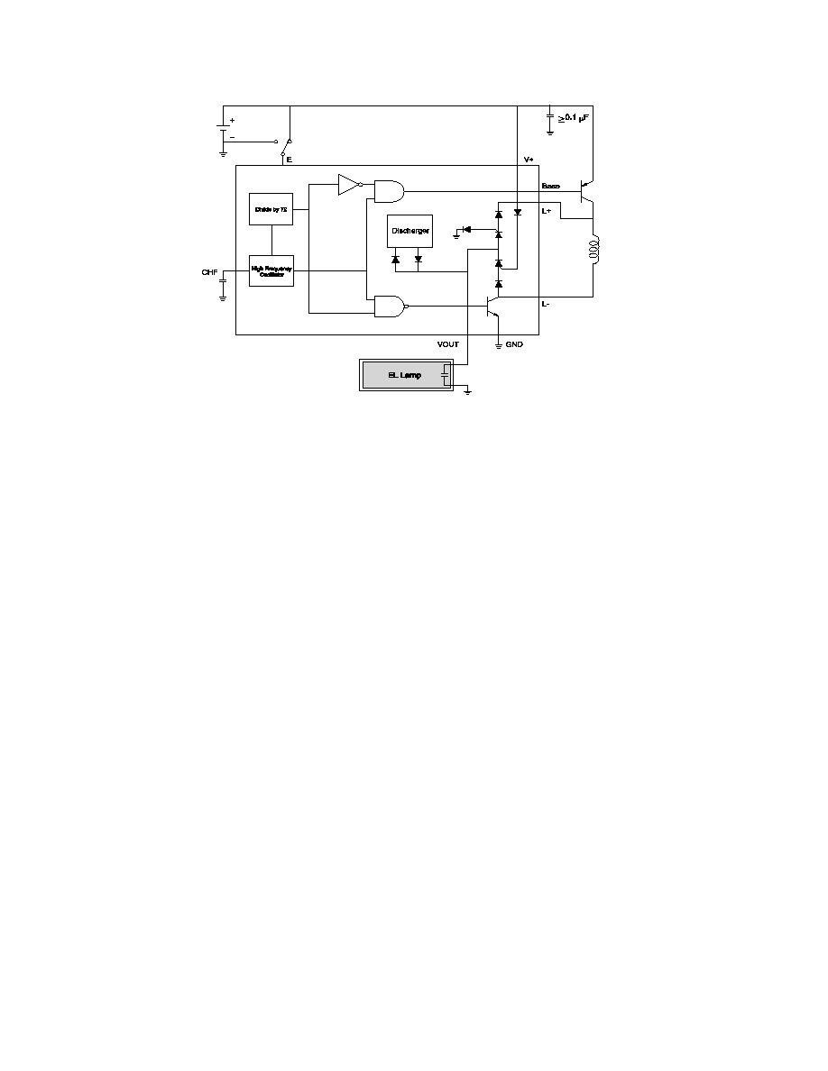
Block Diagram of the Inverter Circuitry
Block Diagram of the Inverter Circuitry
Block Diagram of the Inverter Circuitry
Block Diagram of the Inverter Circuitry
Block Diagram of the Inverter Circuitry
Electroluminescent (EL) lamps are essentially capacitors with one transparent electrode and a special phosphor material
in the dielectric. When a strong AC voltage is applied across the EL lamp electrodes, the phosphor glows. The
required AC voltage is typically not present in most systems and must be generated from a low voltage DC source.
Durel developed its patented 3-Port (3P) switch-mode inverter circuit to convert the available DC supply to an optimal
drive signal for high brightness and low-noise EL lamp applications. The Durel 3P topology offers the simplicity of a
single DC input, single AC output, and a shared common ground that provides an integrated EMI shielding.
The D365 drives the EL lamp by repeatedly pumping charge through an external inductor with current from a DC
source and discharging into the capacitance of the EL lamp load. With each high frequency (HF) charging cycle the
voltage on the lamp is increased. After 32 HF charging cycles, the lamp voltage is discharged to ground in the period
of 4 HF cycles. Then, the polarity of the inductive charging is reversed, and the charging and discharging cycles are
repeated. By this means, a low frequency alternating positive and negative voltage is developed at the single output
lead of the device to one of the electrodes of the EL lamp. Commonly connected to ground, the other lamp electrode
can then be considered as electrical shielding for any underlying circuitry in the application.
The EL driving system is divided into several parts: on-chip logic and control, on-chip high voltage output circuitry,
discharge logic circuitry, and off-chip components. The on-chip logic controls the lamp operating frequency (LF), as
well as the inductor switching frequency (HF), and the HF and LF duty cycles. These signals are combined and
buffered to drive the high voltage output circuitry. The output circuitry handles the power through the inductor and
delivers the high voltage to the lamp. The integrated discharge logic circuit enables the low-noise functionality of this
EL driver. The selection of off-chip components provides a degree of flexibility to accommodate various lamp sizes,
system voltages, and brightness levels. Since a key objective of EL driver systems is to save space and cost, required
off-chip components were kept to a minimum.
Durel provides a D365 Designer's Kit, which includes a PC board intended to aid you in developing an EL lamp driver
configuration using the D365 that meets your requirements. A section on designing with the D365 is included in this
datasheet to serve as a guide to help you select the appropriate external components to complete your D365 EL driver
system.
Typical D365 configurations for driving EL lamps in various applications are shown on the following page. The
expected system outputs, such as lamp luminance, lamp output frequency and voltage, and average supply current
draw, for the various circuit configurations are also shown with each respective figure.
Theory of Operation
Theory of Operation
Theory of Operation
Theory of Operation
Theory of Operation

5
Typical D365A EL Driver Configurations
Typical D365A EL Driver Configurations
Typical D365A EL Driver Configurations
Typical D365A EL Driver Configurations
Typical D365A EL Driver Configurations
3.3V Handset LCD
3.3V Handset LCD
3.3V Handset LCD
3.3V Handset LCD
3.3V Handset LCD
Typical Output
Typical Output
Typical Output
Typical Output
Typical Output
Luminance = 6.1 fL (21 Cd/m
2
)
Lamp Frequency = 278Hz
Supply Current = 13mA
Vout = 190 Vpp
Load = 2in
2
DurelÆ 3 Green EL
5.0V LCD Backlight
5.0V LCD Backlight
5.0V LCD Backlight
5.0V LCD Backlight
5.0V LCD Backlight
Typical Output
Typical Output
Typical Output
Typical Output
Typical Output
Luminance = 7.1 fL (24.3 Cd/m
2
)
Lamp Frequency = 353 Hz
Supply Current = 34 mA
Vout = 190 Vpp
Load = 6in
2
DurelÆ 3 Green EL
3.3V Handset LCD and Keypad
3.3V Handset LCD and Keypad
3.3V Handset LCD and Keypad
3.3V Handset LCD and Keypad
3.3V Handset LCD and Keypad
Typical Output
Typical Output
Typical Output
Typical Output
Typical Output
Luminance = 6.2 fL (21.2 Cd/m
2
)
Lamp Frequency = 246 Hz
Supply Current = 34 mA
Vout = 204 Vpp
Load = 4in
2
DurelÆ 3 Green EL
1
2
3
4
8
7
6
5
L+
VOUT
V+
GND
L-
CHF
E
1.5mH
Sumida CLS62-152
D365
3.3 V
BASE
4 in
2
EL Lamp
0.1
µ
F
MMBTA56
pnp SMT
3.3 V
18 kHz CLK, 25% Duty
OFF
ON
gnd
3.3V
E
GND
VOUT
L-
1
2
3
4
8
7
6
5
L+
V+
CHF
4.7 mH
Coilcraft
DS1608BL-475
D365
3.3 V
BASE
2 in
2
EL Lamp
6.8 nF
0.1
µ
F
MMBTA56
pnp SMT
3.3 V
OFF
ON
1
2
3
4
8
7
6
5
L+
VOUT
V+
GND
L-
CHF
E
2.2 mH
Bujeon
BDS-4020S
D365
5.0 V
BASE
6 in
2
EL Lamp
6.8 nF
1.0
µ
F
MMBTA56
pnp SMT
5.0 V
OFF
ON

6
I. Lamp Frequency Capacitor (CHF) Selection
Selecting the appropriate value of CHF capacitor will specify the inductor switching frequency (HF) and the lamp
frequency (LF) of the D365 EL driver. A divider circuit in the internal oscillator circuitry of the D365A divides the
inductor switching frequency by 72 to get the lamp frequency (LF = HF/72). Lamp frequencies of 200 ≠ 500 Hz are
typically used for longer EL lamp life. Figure 1 graphically represents the effect of CHF capacitor value on the lamp
frequency oscillator at V+=3.3V. In this example at V+=3.3V, LF = 2000 nF-Hz/CHF.
Alternatively, a high frequency clock input may be connected to the CHF pin of the D365A to specify the output driver
frequency. The internal oscillator circuitry in the D365A divides the input clock frequency by 72 to get the output
frequency. Thus, for example, to get a 250Hz lamp frequency from a D365A, the input clock signal must be 18kHz.
The selection of the capacitor value can also affect the brightness of the EL lamp because of its control of LF and HF.
Although input voltage and lamp size can change EL lamp frequency as well, LF mainly depends on the CHF value
selected or the frequency of the input clock signal to CHF. Figure 2 shows typical brightness of a D365 circuit with
respect to lamp frequency on different EL lamp sizes. In this example, the supply voltage and inductor values were
kept constant while only varying frequency.
1
2
3
4
5
6
7
8
9
100
300
500
700
Lamp Frequency (Hz)
Lamp Luminance (fL)
Figure 2: Luminance vs. Lamp Frequency
(V+ = 3.3V, Durel 3 Green EL Lamp)
Figure 1: Typical Lamp Frequency vs. CLF Capacitor
4in
2
6in
2
2in
2
0
200
400
600
800
1000
1200
1400
0
5
10
15
20
25
CHF (nF)
Lamp Frequency (Hz)
7
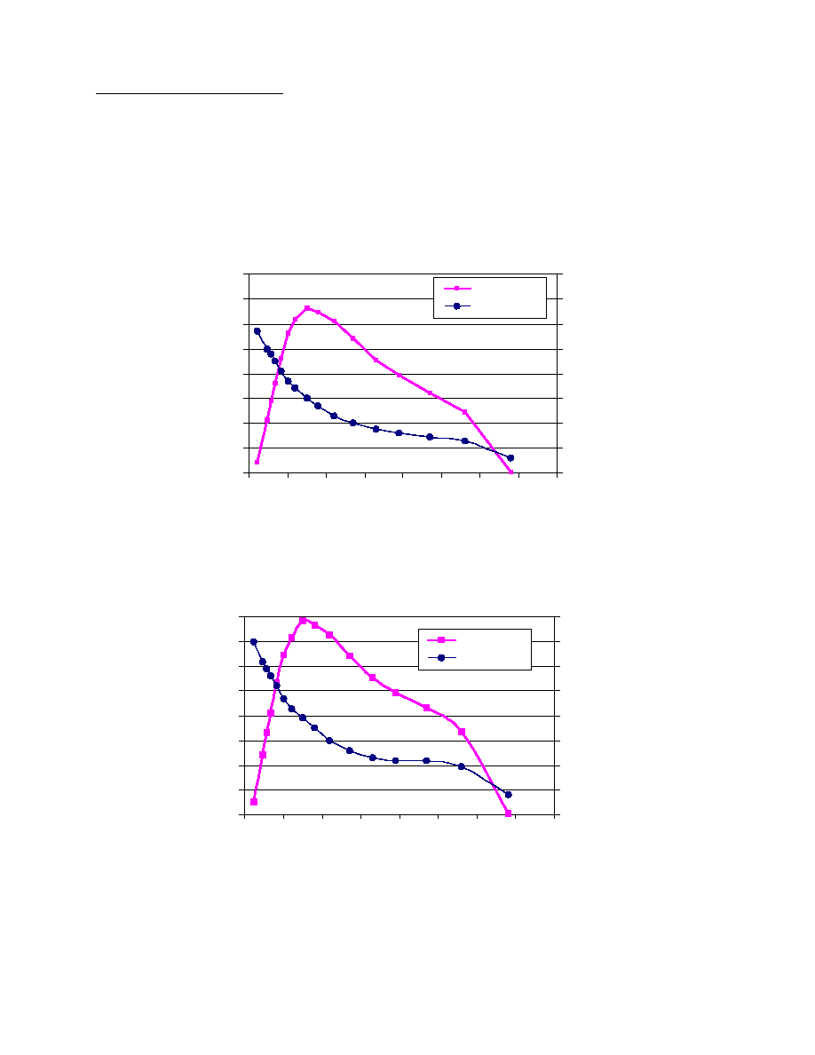
II. Inductor (L) Selection
The external inductor (L) selection for a D365A circuit greatly affects the output capability and current draw of the
driver. A careful designer will balance current draw considerations with output performance in the choice of an ideal
inductor for a particular application. Figures 3 and 4 show typical brightness and current draw of a D365A circuit with
different inductor values, lamp sizes, and supply voltages while keeping HF and LF constant. Please note that the DC
resistance (DCR) of inductors with the same nominal inductance value may vary with manufacturer and inductor type.
Thus, inductors made by a different manufacturer may yield different outputs, but the trend of the different curves
should be similar. Lamp luminance is also a function of lamp size. In each example, a larger lamp will have less
luminance with approximately the same current draw.
Figure 3: Brightness and current vs. inductor value.
(Conditions: V+ = 3.3V, 2 in
2
EL Lamp)
Figure 4: Brightness and current vs. inductor value.
(Conditions: V+ = 5.0V, 4 in
2
EL Lamp)
0
1
2
3
4
5
6
7
8
0
1
2
3
4
5
6
7
8
Inductor (mH)
Luminance (fL)
0
10
20
30
40
50
60
70
80
Current (mA)
Luminance
Current
0
1
2
3
4
5
6
7
8
0
1
2
3
4
5
6
7
8
Inductor (mH)
Luminance (fL)
0
10
20
30
40
50
60
70
80
Current (mA)
Luminance
Current
8
III. PNP Transistor Selection
The D365A requires an external pnp transistor to complete the high voltage 3P circuitry. Ideally, this transistor should
have a minimum collector-emitter breakdown voltage higher than the required peak voltage output of the EL driver. It
should also have a high DC current gain (>50) and fast switching characteristics.
Durel typically recommends the MMBTA56 surface mount amplifier transistor for general purpose because it is a
standard device part number supplied by several large manufacturers. The MMBTA56 has a breakdown voltage that
is normally above 100V although it has a minimum rating of 80V only. The counterpart internal npn transistor in the D365
has a minimum 100V breakdown, with typical breakdown value above 120V. Under most nominal design considerations
using the D365, the MMBTA56 is an appropriate selection. Nevertheless, caution is advised to limit designs well within
the maximum output voltage ratings of all devices to avoid failure of the IC or any required external components.
D365 Design Ideas
D365 Design Ideas
D365 Design Ideas
D365 Design Ideas
D365 Design Ideas
I. Alternate Lamp Connection
In some applications it may be more convenient to connect the EL lamp to the supply voltage rather than ground. This
connection (shown below) provides design flexibility and does not degrade EL driver performance. This configuration
may also be used to minimize any positive DC bias on the lamp.
1
2
3
4
8
7
6
5
L+
VOUT
V+
GND
L-
CHF
E
L
D365
V+
BASE
EL Lamp
CHF
capacitor
0.1
µ
F
pnp transistor
V+
OFF
ON
9
II. Driving Multi-segment Lamps
The D365 may be used to drive multiple EL lamp segments. An external transistor switching circuit is used to turn each
lamp segment on or off independently or simultaneously. A high signal at the corresponding E input will enable the
corresponding lamp segment. In this configuration, EL Lamp 1 is always turned on when the IC is enabled. Otherwise,
always make sure that at least one lamp segment is selected to be on when the D365 is enabled.
1
2
3
4
8
7
6
5
L+
VOUT
V+
GND
L-
CHF
E
L
D365
V+
BASE
CHF
capacitor
0.1
µ
F
pnp transistor
V+
OFF
ON
EL Lamp
Segment 2
EL Lamp
Segment 1
EL Lamp
Segment 3
E2
2.2K
4.7K
BAS21LT1
BAS21LT1
MMBT5401LT1
MMBT5551LT1
1K
E3
2.2K
4.7K
BAS21LT1
BAS21LT1
MMBT5401LT1
MMBT5551LT1
1K
OFF
ON
100 nF
100 nF
OFF
ON
III. Lamp Frequency Control with an External Clock Signal
An external clock signal may be used to control the inductor oscillating frequency (HF) and, consequently, the EL lamp
frequency (LF) of the D365. HF and LF can be varied to synchronize the EL driver with other elements in the
application. An internal divider network in the IC creates a ratio of HF/LF=72.
1
2
3
4
8
7
6
5
L+
VOUT
V+
GND
L-
CHF
E
L
D365
V+
BASE
EL Lamp
0.1
µ
F
pnp transistor
V+
OFF
ON
HF CLK
1.0V Min
0.2V Max
25% +Duty

10
IV. Controlling EL Brightness Through Clock Pulse Width Modulation
Pulse-width modulation of an external clock signal that controls the inductor oscillating frequency may also be used to
regulate the brightness of an EL lamp. In this circuit, when the positive duty cycle of the external clock is at 25%, the
lamp is at full brightness. Incremental dimming occurs as the positive duty cycle is increased to as high as 75%. This
scheme may also be used inversely to regulate lamp brightness over the life of the battery or to compensate for lamp
aging. In these cases, positive duty cycle may be incrementally increased as part of a feedback control in the application.
(Note: Operation at duty cycles higher than 75% or lower than 25% is not recommended.)
1
2
3
4
8
7
6
5
L+
VOUT
V+
GND
L-
CHF
E
L
D365
V+
BASE
EL Lamp
0.1
µ
F
pnp transistor
V+
OFF
ON
HF CLK
1.0V Min
0.2V Max
V. Two-Level Dimming Control
Two level dimming may be achieved with the circuit below. When DIM is low, the external PNP transistor is saturated
and the EL lamp runs at full brightness. When DIM is high, the external PNP turns off and the 47
resistor reduces the
voltage at (V+) and dims the EL lamp.
1
2
3
4
8
7
6
5
L+
VOUT
V+
GND
L-
CHF
E
L
D365
BASE
EL Lamp
CHF
capacitor
0.1
µ
F
pnp transistor
V+
OFF
ON
V
bat
47
1k
DIM
2N3906

11
VI. High EL Brightness Through Supply Voltage Doubling
An external voltage boost circuit may be used to increase the voltage supplied to the D365. In the following circuit, the
National Semiconductor LM2661 is used as a positive voltage doubler.
1
2
3
4
8
7
6
5
L+
VOUT
V+
GND
L-
CHF
E
L
D365
BASE
EL Lamp
CHF
capacitor
pnp transistor
V+
OFF
ON
LM 2661
Vin
SD
CAP+
GND
CAP-
V+
OSC
LV
OUT
1N5817
47uF
47uF
10uF
VII. EL Lamp Brightness Regulation
Regulating the DC supply input voltage to the D365 will result in a constant brightness level from the EL lamp,
regardless of battery voltage. In this example, a Micrel voltage regulator is used.
1
2
3
4
8
7
6
5
L+
VOUT
V+
GND
L-
CHF
E
L
D365
Vbat
BASE
EL Lamp
CHF
capacitor
0.1
µ
F
pnp transistor
V+
OFF
ON
1 GND
2 E
OUT
IN
4
3
MIC5203
E
12
DUREL Corporation
2225 W. Chandler Blvd.
Chandler, AZ 85224-6155
Tel: (480) 917-6000
FAX: (480) 917-6049
Website: http://www.durel.com
The DUREL name and logo are registered trademarks of DUREL CORPORATION.
This information is not intended to and does not create any warranties, express or implied, including any warranty of merchantability
or fitness for a particular purpose. The relative merits of materials for a specific application should be determined by your evaluation.
The EL driver circuits herein are covered by one or more of the following U.S. patents: #5,313,141; #5,347,198; #5,789,870.; #5,780,975; #6,043,610.
Corresponding foreign patents are issued and pending.
ISO 9001 Certified
© 2000, 2001 Durel Corporation
Printed in U.S.A.
LIT-I 9035 Rev. A04
The D365A IC is available as bare die in probed wafer form or in die tray, and in standard MSOP-8 plastic package per
tube or per tape and reel. A Durel D365A Designer's Kit (1DDD365AA-K01) provides a vehicle for evaluating and
identifying the optimum component values for any particular application using D365A. Durel engineers also provide
full support to customers, including specialized circuit optimization and application retrofits.
MSOPs in Tubes: 1DDD365AA-M01
MSOPs in Tubes: 1DDD365AA-M01
MSOPs in Tubes: 1DDD365AA-M01
MSOPs in Tubes: 1DDD365AA-M01
MSOPs in Tubes: 1DDD365AA-M01
MSOPs in Tape & Reel: 1DDD365AA-M02
MSOPs in Tape & Reel: 1DDD365AA-M02
MSOPs in Tape & Reel: 1DDD365AA-M02
MSOPs in Tape & Reel: 1DDD365AA-M02
MSOPs in Tape & Reel: 1DDD365AA-M02
MSOPs are marked with part number (365A) and 3-digit wafter lot
code. Bottom of marking is on the Pin 1 side.
Ordering Information:
Ordering Information:
Ordering Information:
Ordering Information:
Ordering Information:
A
0.94
0.037
1.02
0.040
1.09
0.043
B
0.05
0.002
0.10
0.004
0.15
0.006
C
0.20
0.008
0.33
0.013
0.46
0.018
D
0.41
0.016
0.53
0.021
0.65
0.026
E
0.13
0.005
0.18
0.007
0.23
0.009
F
2.84
0.112
3.00
0.118
3.15
0.124
G
0.43
0.017
0.65
0.026
0.83
0.033
H
4.70
0.185
4.90
0.193
5.11
0.201
I
2.84
0.112
3.00
0.118
3.25
0.128
mm.
in.
mm.
in.
mm.
in.
MSOP-8
MSOP-8
MSOP-8
MSOP-8
MSOP-8
Min.
Typical
Max.
Tape Orientation
Tube-length = 320 mm (12.6 in). 100 units per
tube.
Embossed tape on 360 mm diameter reel per E1A-481-2.
2500 units per reel. Quantity marked on reel label.
F
H
I
A
B
G
C
D
E