
DM9102
10/100Mbps Single Chip LAN Controller
Final
1
Version: DM9102-DS-F03
August 30,2000
T
General Description
The DAVICOM
'
s DM9102 is a highly integrated single-
chip Fast Ethernet controller. It fully integrated 100BASE-
TX/10Base-T Fast Ethernet MAC, PHY and PMD. It is
fully compliant with PCI Spec. 2.1 and IEEE802.3u.
The DM9102 provides a direct interface to the PCI local
bus and direct connection to the network wire. As a
controller, it provides the bus master capability. The
DM9102 also supports auto-negotiation function that
enables it to detect speed and duplex automatically. Due
to the well-controlled rising/falling time, it requires no
external filter to transmit signal to the media.
T
Block Diagram
D M A
E E P R O M
Interface
B o o t R O M
Interface
P C I
Interface
TX+/-
RX+/-
M I I M a n a g e m e n t C o n t r o l
& M I I R e g i s t e r
A u t o n e g o t i a t i o n
L E D D r i v e r
R X
M a c h i n e
R X
F I F O
T X
F I F O
T X
M a c h i n e
M A C
M I I
N R Z t o N R Z I
N R Z I t o M L T 3
Parallel to
Serial
Scrambler
4 B / 5 B
Encoding
M L T 3 t o N R Z I
N R Z I t o N R Z
Parallel to
Serial
D e -
Scrambler
4 B / 5 B
D e c o d i n g
A E Q
P H Y c e i v e r

DM9102
10/100Mbps Single Chip LAN Controller
2
Final
Version: DM9102-DS-F03
August 30, 2000
Table of Contents
General Description ................................................1
Block Diagram ........................................................1
Features .................................................................4
Pin Configuration: DM9102 QFP .............................5
Pin Description .......................................................6
- PCI Bus Interface ................................................6
- Boot ROM and EEPROM Interface ......................7
Multiplex Mode ...................................................7
Direct Mode .........................................................8
- LED Pins .............................................................9
- Network Interface ..............................................10
- Clock Pins .........................................................10
- Miscellaneous Pins ............................................10
- Power Pins ........................................................11
Register Definition ................................................12
PCI Configuration Registers ..............................12
Key to Default .......................................................13
Identification ID..................................................14
Command & Status............................................14
Command Register Definition ............................16
Revision ID........................................................17
Miscellaneous Function .....................................17
I/O Base Address...............................................18
Memory Mapped Base Address .........................18
Subsystem Identification ....................................19
Expansion ROM Base Address..........................19
Capabilities Pointer............................................20
Interrupt & Latency Configuration.......................20
Device Specific Configuration Register ..............20
Control and Status Register (CR)......................22
Key to Default .......................................................22
1. System Control Register (CR0) .........................23
2. Transmit Descriptor Poll Demand (CR1)............24
3. Receive Descriptor Poll Demand (CR2) ............24
4. Receive Descriptor Base Address (CR3) ...........24
5. Transmit Descriptor Base Address (CR4) ..........25
6. Network Status Report Register (CR5)..............25
7. Network Operation Register (CR6) ....................27
8. Interrupt Mask Register (CR7)...........................29
9. Statistical Counter Register (CR8).....................30
10. PROM & Management Access Register (CR9) 31
11. Programming ROM Address Register (CR10) .32
12. General Purpose Timer Register (CR11) .........32
13. PHY Status Register (CR12)........................... 32
14. Frame Access Register................................... 33
15. Frame Data Register (CR14) .......................... 33
16. Watching & Jabber Timer Register (CR15) ..... 33
PHY Management Register Set ........................ 34
Key To Default ..................................................... 34
Basic Mode Control Register (BMCR)
- Register 0 .......................................................... 35
Basic Mode Status Register (BMSR)
- Register 1 .......................................................... 36
PHY ID Identifier Register #1 (PHYIDR1)
- Register 2 .......................................................... 37
PHY ID Identifier Register #2 (PHYIDR2)
- Register 3 .......................................................... 37
Auto-negotiation Advertisement Register (ANAR)
- Register 4 .......................................................... 37
Auto-negotiation Link Partner Ability Register
(ANLPAR) - Register 5 ......................................... 38
Auto-negotiation Expansion Register (ANER)
- Register 6 .......................................................... 39
DAVICOM Specified Configuration Register (DSCR)
- Register 16......................................................... 39
DAVICOM Specified Configuration and Status
Register (DSCSR) - Register 17 ........................... 40
10Base-T Configuration/Status (10BTSCRCSR)
- Register 18......................................................... 41
Functional Description .......................................... 42
System Buffer Management .............................. 42
1. Overview .......................................................... 42
2. Data Structure and Descriptor List .................... 42
3. Buffer Management: Ring Structure Method ..... 42
4. Buffer Management: Chain Structure Method ... 43
5. Descriptor List: Buffer Descriptor Format .......... 43
(a). Receive Descriptor Format ............................. 43
(b). Transmit Descriptor Format ............................ 45

DM9102
10/100Mbps Single Chip LAN Controller
Final
3
Version: DM9102-DS-F03
August 30,2000
Initialization Procedure..........................................48
Data Buffer Processing Algorithm..........................48
1. Receive Data Buffer Processing ........................48
2. Transmit Data Buffer Processing .......................49
Network Function ..............................................50
1. Overview...........................................................50
2. Receive Process and State Machine .................50
3. Transmit Process and State Machine ................50
4. Physical Layer Overview ...................................50
Serial Management Interface.............................51
Configuration ROM Overview................................52
1. Subsystem ID Block ..........................................52
2. CROM Version..................................................53
3. Controller Count................................................53
4. Controller_X Information ...................................53
5. Controller Information Body Pointed By
Controller_X Info Block Offset Item in Controller
Information Header ............................................53
Absolute Maximum Ratings...................................55
DC Electrical Characteristics .................................55
AC Electrical Characteristics & Timing Waveforms 56
PCI Clock Spec. Timing.....................................56
Other PCI Signals Timing Diagram ....................56
Multiplex Mode Boot ROM Timing......................57
Direct Mode Boot ROM Timing ..........................57
EEPROM Timing ...............................................58
PHYceiver .........................................................58
Auto-negotiation and Fast Link Pulse Timing
Diagram ............................................................59
Package Information.............................................60
Ordering Information.............................................61
Disclaimer ............................................................61
Company Overview ..............................................61
Products ...............................................................61
Contact Windows..................................................61
Warning................................................................61
Appendix A ...........................................................62
DM9102 SROM Format.....................................62

DM9102
10/100Mbps Single Chip LAN Controller
4
Final
Version: DM9102-DS-F03
August 30, 2000
T
Features
T
Single chip LAN controller integrated Fast Ethernet MAC,
PHY and transceiver
T
Compliant with IEEE 802.3u 100BASE-TX, IEEE 802.3
10BASE-T and ANSI X3T12 TP-PMD standard
T
Direct interface to the PCI bus & fully compliant with PCI
specification 2.1
T
PCI bus master architecture
T
Support PCI bus burst mode data transfer with
programmable burst size
T
EEPROM 93C46 interface to store configuration
information and user defined message
T
Support up to 256K bytes Boot ROM interface
T
Two large independent receive FIFO (4K) & transmit
FIFO (2K) with programmable FIFO threshold and full
packet burst processing
T
Support automatic packet deletion for runt packets and
packet re-transmission with no FIFO reload
T
Support Full/Half Duplex operation
T
Physical, broadcast address recognition and 512-bit hash
table algorithm for multicast address filtering
T
Compliant with IEEE802.3u Auto-negotiation protocol for
automatic link type selection
T
High performance 100Mbps clock generator and data
recovery circuit
T
Digital clock recovery circuit using advanced digital
algorithm to reduce jitter
T
Adaptive equalization circuit and Baseline wandering
restoration circuit for 100Mbps receiver
T
Provides Loopback mode for easy system diagnostics
T
128 pin QFP with CMOS process
DM9102
10/100Mbps Single Chip LAN Controller
Final
5
Version: DM9102-DS-F3
August 30, 2000
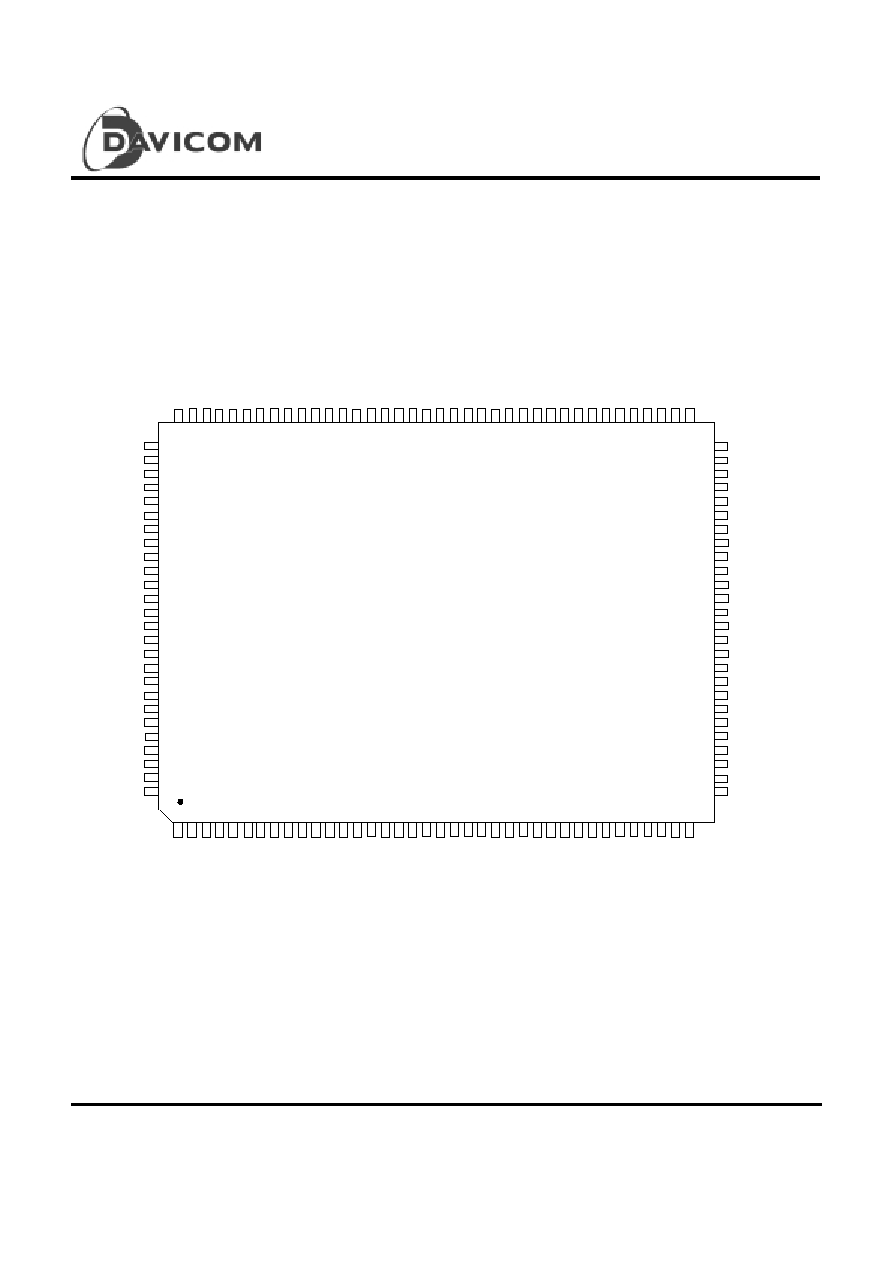
T
Pin Configuration
11
DM9102
80
79
78
77
76
75
74
73
72
71
70
69
68
67
66
65
6 4
6 3
6 2
6 0
5 9
5 8
5 7
5 6
5 0
4 9
4 8
4 7
4 6
4 5
4 4
4 3
4 2
4 1
4 0
3 9
38
37
36
35
34
33
32
31
90
91
92
93
94
95
96
97
98
99
100
1
2
3
4
5
6
7
8
9
10
12
13
14
15
16
17
18
19
20
21
22
23
24
25
26
28
29
30
5 5
5 4
5 3
5 2
5 1
6 1
81
82
83
84
85
86
87
88
89
I N T #
R S T #
DVDD
GNT#
REQ#
PCLK
AD31
AD30
AD29
AD28
AD27
AD26
AD25
AD24
CBE3#
DGND
NC
IDSEL
AD23
AD21
AD20
AD19
AD18
AD17
AD16
CBE2#
AD22
DVDD
DGND
FRAME#
S T O P #
IRDY#
TRDY#
D E V S E L #
P E R R #
S E R R #
C B E 0 #
B G G N D
B G R E S
O S C V D D
X 1 / O S C
X 2
O S C G N D
LEDTRF
LEDFDX
LED100M
D G N D
LED10M
BPA0
BPA1/TEST
EEDI
EEDO
EECK
EECS
SELROM
TEST0
TEST1
TEST2
BPAD4
BPAD5
BPAD6
BPAD7
BPCS#
BPAD0
BPAD1
BPAD2
BPAD3
AD0
AD1
AD2
A D 6
A D 7
DVDD
A D 5
AD3
DGND
AD4
A D 9
A D 1 0
D G N D
A D 1 1
D V D D
A D 1 3
A D 1 4
A D 1 5
A D 1 2
A D 8
C B E 1 #
P A R
(MA10/LEDTRF)
(MA11/LEDFDX)
(MA12/LED100M)
(MA13LED10M)
(MD0/EEDI)
(MD1)
(MD2)
(MD3)
(MD4)
(MD5)
(MD6)
(MD7)
(ROMCS)
(MA0)
(MA1)
(MA2)
(MA3/EEDO)
(MA4/EECK)
(MA5)
(MA6/SELROM)
(MA7)
(MA8)
(MA9)
D V D D
D G N D
DGND
DVDD
DGND
DVDD
DVDD
DGND
DGND
DVDD
27
D V D D
D V D D
D G N D
D V D D
D G N D
D G N D
DVDD
DGND
DGND
DVDD
MA16
102
101
MA15
MA14
1 0 3
1 0 4
1 0 5
1 0 6
1 0 7
1 0 8
1 0 9
1 1 0
1 1 1
1 1 2
1 1 3
1 1 4
1 1 5
1 1 6
1 1 7
1 1 8
1 1 9
1 2 0
1 2 1
1 2 2
1 2 3
1 2 4
1 2 5
1 2 7
1 2 8
1 2 6
D G N D
D V D D
P W R I N
R A V D D
R X I -
R X I +
R A G N D
T A G N D
T X O -
T X O +
T A V D D
T A G N D
T A G N D
T A G N D
T A V D D
NC
NC
NC
NC