 | –≠–ª–µ–∫—Ç—Ä–æ–Ω–Ω—ã–π –∫–æ–º–ø–æ–Ω–µ–Ω—Ç: EB-120 | –°–∫–∞—á–∞—Ç—å:  PDF PDF  ZIP ZIP |

ATA-120
This is preliminary information on a new product. Specifications are subject to change without notice.
129 Morgan Drive, Norwood, MA 02062 voice: (781) 551-9450
fax: (781) 440-9528 email: apogee@apogeeddx.com
CONTROLLED DOCUMENT: P_903-000009_Rev14 ATA-120 Data Sheet.doc
DRN: PRELIMINARY Page 1 of 13
20W Class D Single Channel Audio Amplifier
FEATURES
∑
HIGH OUTPUT POWER CAPABILITY
∑
SINGLE SUPPLY (+7.5V to +24V)
∑
THD+N < 0.05% @ 1W, 8
∑
HIGH EFFICIENCY, > 90% @ 4
, 20W
∑
LOW QUIESCENT CURRENT, 13mA
∑
LOW NOISE (190µV typ.)
∑
POP ELIMINATION AT STARTUP AND
SHUTDOWN
∑
BUILT-IN THERMAL PROTECTION
∑
INTEGRATED SHORT CIRCUIT PROTECTION
∑
180m
MOSFET SWITCHES
∑
MUTE / STANDBY MODE
∑
SMALL SMD PACKAGE IS
BOTH LEAD-FREE (Pb) AND GREEN
APPLICATIONS
∑
TELEVISIONS
∑
HOME AUDIO MINI-SYSTEMS
∑
FLAT PANEL MONITORS
∑
MULTIMEDIA SPEAKERS
∑
SURROUND SOUND DVD SYSTEMS
1.0 GENERAL DESCRIPTION
The ATA-120 Class-D Audio Amplifier is a fully
integrated monolithic audio amplifier that can
provide audio power up to 20 watts @ 10% THD into
a 4
speaker.
The ATA-120 incorporates a single ended output
structure with built-in short circuit and
overtemperature protection. This low noise, high
performance device delivers the excellent audio
quality of a class A/B amplifier while still achieving
class-D efficiency greater than 90%.
ORDERING INFORMATION:
Part Number * Package
Temperature
ATA-120
SOIC8
-40∞C to + 85∞C
EB-120
Evaluation Board for the ATA-120
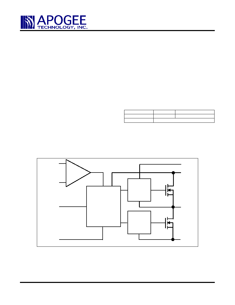
Figure 1 - Block Diagram
ENABLE
IN_N
IN_P
AGND
FET
DRIVE
FET
DRIVE
PGND
POUT
VDD
BOOST
+
-
REGULATOR,
CONTROL &
PROTECTION

ATA-120
This is preliminary information on a new product. Specifications are subject to change without notice.
129 Morgan Drive, Norwood, MA 02062 voice: (781) 551-9450
fax: (781) 440-9528 email: apogee@apogeeddx.com
CONTROLLED DOCUMENT: P_903-000009_Rev14 ATA-120 Data Sheet.doc
DRN: PRELIMINARY Page 2 of 13
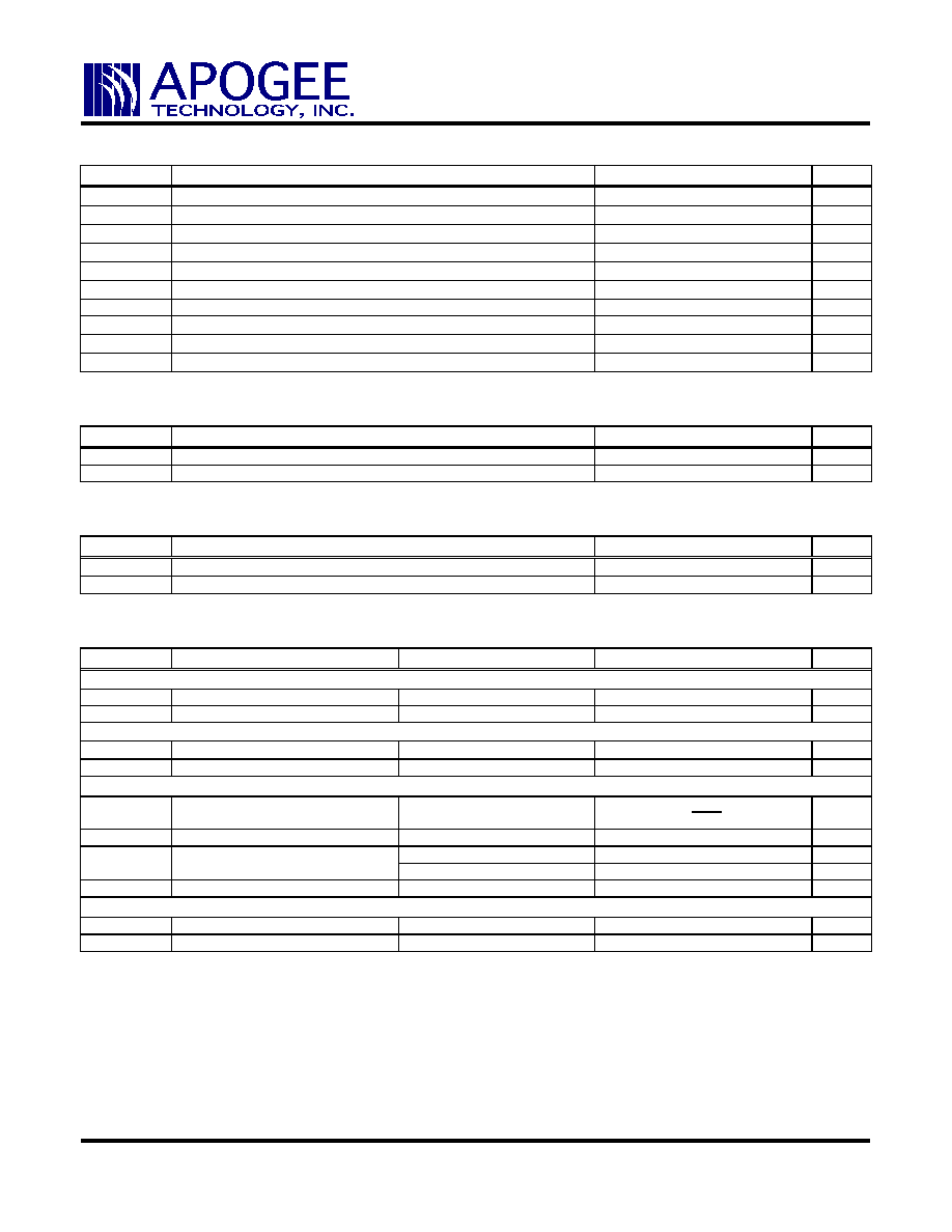
Absolute Maximum Ratings [Note 1]
SYMBOL PARAMETER MIN
TYP
MAX
UNIT
V
DD
Supply Voltage
26
V
V
BOOST
Bootstrap Voltage
V
OUT
-0.3
V
OUT
+6.5
V
V
ENABLE
Enable Voltage
-0.3
6.0
V
V
OUT
Output Switch
-1
V
DD
+1 V
V
IN_P
Positive Input
-1
V
DD
+1 V
V
IN_N
Negative Input
-1
V
DD
+1 V
-
Analog GND to Power GND
-0.3
0.3
V
T
j
Junction Temperature
150 ∞C
T
LEADS
Lead Temperature
260 ∞C
T
S
Storage Temperature
-65
150 ∞C
Note 1 ≠ Operation above maximum ratings may damage the device.
1.1 Recommended Operating Conditions [Note 2]
SYMBOL PARAMETER MIN
TYP
MAX
UNIT
V
DD
Supply Voltage
7.5
24
V
T
A
Operating
Temperature
-40
85
∞C
Note 2 - Performance not guaranteed beyond recommended operating conditions.
1.2 Thermal
Characteristics
SYMBOL PARAMETER MIN
TYP
MAX
UNIT
J-A
Thermal Resistance, Junction to Ambient
105
∞C/W
J-C
Thermal Resistance, Junction to Case [Note 3]
50
∞C/W
Note 3 ≠ Solder pins directly to large copper surface areas to improve device cooling.
1.3 Electrical
Characteristics [Note 4]
SYMBOL PARAMETER
CONDITION MIN
TYP
MAX
UNIT
Supply Current
I
STBY
Standby
Current
V
ENABLE
= 0
130
µA
I
Q
Quiescent
Current
13
mA
Output Drivers
R
DS-ON
Output MOSFET on Resistance
Sourcing and Sinking
0.18
I
SC
Short Circuit Current
Sourcing and Sinking
3
5
A
Inputs
V
IN
IN_P, IN_N Input
Common Mode Voltage Range
0
VDD
2
VDD-1.5 V
I
IN
IN_P, IN_N Input Current
1
5
µA
Rising signal voltage
1.4
2.0
V
V
ENABLE
Enable Threshold Voltage
Falling signal voltage
0.4
1.2
I
ENABLE
Enable Input Current
V
ENABLE
= 5V
1
µA
Thermal Shutdown
T
SD
Thermal Shutdown Trip Point
T
J
Rising
150
∞C
T
SD-HYS
Thermal Shutdown Hysteresis
30
∞C
Note 4 ≠ Performance based on circuit in Figure 3, V
DD
= 24V, V
ENABLE
= 5V, T
A
= 25∞C

ATA-120
This is preliminary information on a new product. Specifications are subject to change without notice.
129 Morgan Drive, Norwood, MA 02062 voice: (781) 551-9450
fax: (781) 440-9528 email: apogee@apogeeddx.com
CONTROLLED DOCUMENT: P_903-000009_Rev14 ATA-120 Data Sheet.doc
DRN: PRELIMINARY Page 3 of 13
1.4 Typical Operating Characteristics [Note 5]
SYMBOL PARAMETER
CONDITION
MIN
TYP MAX UNIT
THD+N = 10%
, 4
Load
20 W
P
OUT
Power Output
THD+N = 10%
, 8
Load
10 W
P
OUT
= 1 W
, 4
Load
0.1 %
THD+N
Total Harmonic Distortion
Plus Noise
P
OUT
= 1 W
, 8
Load
0.05 %
P
OUT
= 20 W,
4
Load
90 %
Efficiency
P
OUT
= 10 W, 8
Load
93 %
BW
Maximum Power Bandwidth
20
KHz
DNR Dynamic
Range
A-Weighted
91
dB
SNR
Signal to Noise Ratio
A-Weighted, relative to 15W
92
dB
Noise
Floor
A-Weighted
190
µV
PSR
Power Supply Rejection
47
dB
Note 5 ≠ Performance based on circuit of Figure 3, V
DD
= 24V, V
ENABLE
= 5V, f = 1 KHz, T
A
= 25∞C
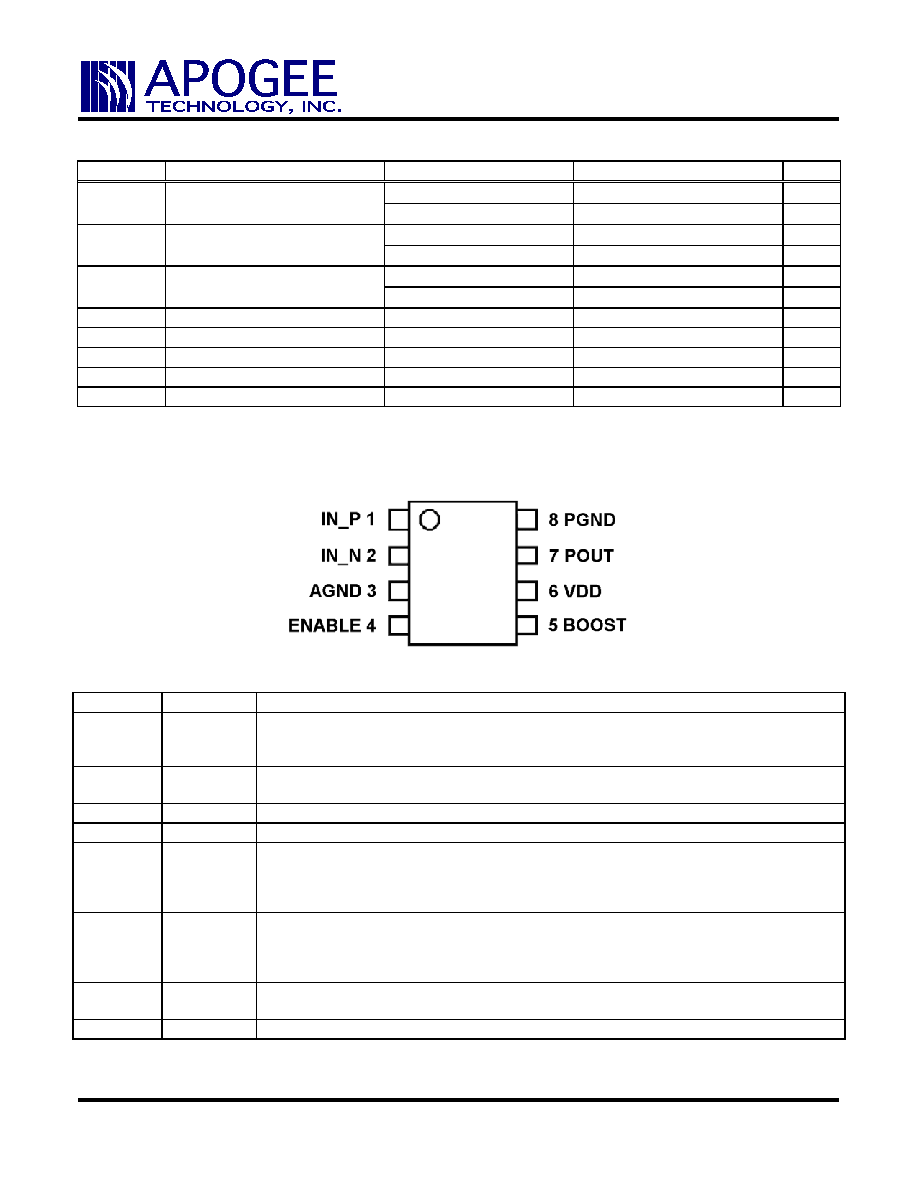
2.0 PIN DESCRIPTION
Pin No.
Pin Name Pin Function
1 IN_P
Amplifier Positive Input. IN_P is the positive side of the differential input to the
amplifier. Use a resistive voltage divider to set the voltage at IN_P to V
DD
/2. See
Figure 3
.
2 IN_N
Amplifier Negative Input. IN_N is the negative side of the differential input to the
amplifier. Drive the input signal and close the feedback loop at IN_N. See
Figure 3
.
3 AGND
Analog Ground. Signal input ground. Connect AGND to PGND at one single point.
4 ENABLE
Enable Input. Set ENABLE high to turn-on the amplifier; set it low to turn it off.
5 BOOST
High-Side MOSFET Bootstrap Input. A capacitor from BOOST to POUT supplies
the gate drive current to the high-side of the MOSFET. Connect a 0.47µF capacitor
from POUT to BOOST. Place a 6.2V zener diode from BOOST to POUT to prevent
overstressing the internal circuitry.
6 VDD
Power Supply Input. VDD is the drain of the high-side MOSFET switch and supplies
the power to both the output stage and the ATA-120 internal control circuitry. In
addition to the main bulk capacitor, bypass VDD to PGND with a 1µF X7R capacitor
placed close to the IC's V
DD
(pin 6) and P
GND
(pin 8).
7 POUT
Switched Power Output. POUT is the output of the ATA-120. Connect the L-C filter
between POUT and the output blocking capacitor. See
Figure 3
.
8 PGND
Power Ground. Power stage ground. Connect PGND to AGND at one single point.

ATA-120
This is preliminary information on a new product. Specifications are subject to change without notice.
129 Morgan Drive, Norwood, MA 02062 voice: (781) 551-9450
fax: (781) 440-9528 email: apogee@apogeeddx.com
CONTROLLED DOCUMENT: P_903-000009_Rev14 ATA-120 Data Sheet.doc
DRN: PRELIMINARY Page 4 of 13
3.0 Functional Description
The ATA-120 is a single-ended Class-D audio amplifier that converts analog audio input signals into PWM pulses.
The pulses drive an internal high current output stage and, when filtered through an external L-C filter, reproduce
the input signal across the load. Because of the switching Class-D output stage, power dissipation in the amplifier
is drastically reduced compared to Class A, Class B or Class A/B amplifiers while maintaining high fidelity and low
distortion.
The amplifier uses a differential input to the modulator. IN_P is the positive input and IN_N is the negative input.
The common mode voltage of the input is set to half the DC power supply input voltage (V
DD
/2) through the
resistive voltage divider formed by R2 and R5. The input capacitor C3 couples the AC input signal into the
amplifier while blocking the DC component.
The output driver stage uses two 180 m
N-channel MOSFETs to deliver the pulses to the L-C output filter which
in turn drives the load. When the output switches low, the bootstrap capacitor, C9, which is located between
POUT and BOOST, is charged from VDD through internal circuitry inside the ATA-120. The gate of the upper
MOSFET is driven from this voltage (higher than VDD but clamped to safe levels by zener diode D2).
3.1 Pop
Elimination
The DC-blocking capacitor, C38, allows only AC current to pass to the output load (speaker). To insure that the
amplifier properly passes low frequency signals, the time constant of C38*R
LOAD
needs to be long. Typically the
C11 capacitor charges over a long time period and would normally result in turn-on and/or turn-off "pops". The
ATA-120, however, includes internal circuitry that eliminates the turn-on and turn-off pops associated with this
charging of the AC coupling capacitor.
3.2 Short Circuit/Overload Protection
The ATA-120 has internal overload and short circuit protection. The currents in both the high-side and low-side
MOSFETs are internally measured and if the current exceeds the 5A (typical) short circuit current limit on either
MOSFET, both MOSFETs are placed in an open condition. After the short circuit condition is removed, the
ATA-120 restarts with the same power up sequence that is used for normal starting to prevent a pop from
occurring.
3.3 Mute/Enable
Function
The ENABLE input is an active high enable control. To enable the device, drive ENABLE with a 2.0V or greater
voltage. To disable the amplifier, drive it below 0.4V. While the device is disabled, the VDD operating current is
less than 130µA and the output MOSFETs are turned off. The ATA-120 requires approximately 500ms from the
time that ENABLE is asserted (driven high) to when the amplifier arrives at normal operation.

ATA-120
This is preliminary information on a new product. Specifications are subject to change without notice.
129 Morgan Drive, Norwood, MA 02062 voice: (781) 551-9450
fax: (781) 440-9528 email: apogee@apogeeddx.com
CONTROLLED DOCUMENT: P_903-000009_Rev14 ATA-120 Data Sheet.doc
DRN: PRELIMINARY Page 5 of 13
4.0 Power Output
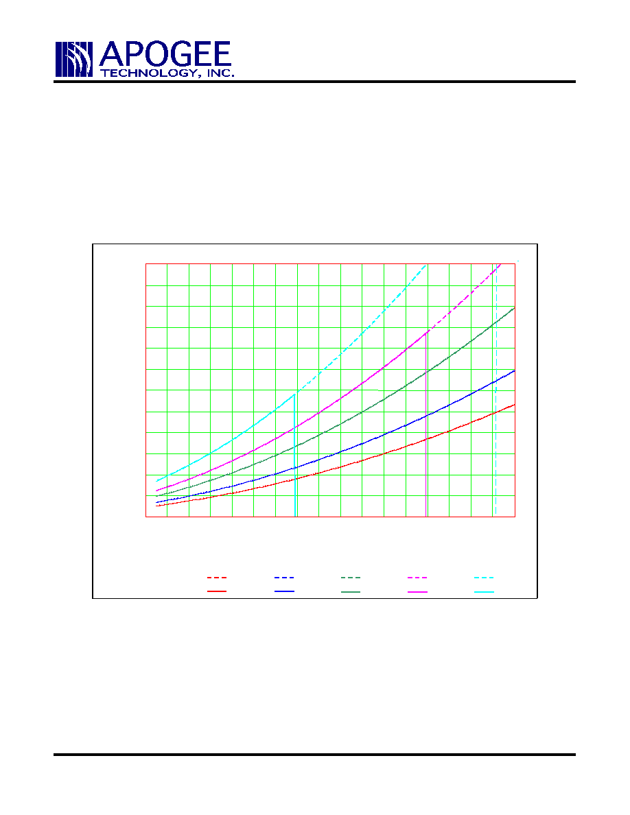
Figure 2 shows the full-scale sine-wave output power as a function of Power Supply Voltage for 2, 3, 4, 6, and 8
Ohm loads. Output power is constrained for higher impedance loads by the maximum voltage limit of the
ATA-120 and by the over-current protection limit for lower impedance loads. The minimum threshold for the over-
current protection circuit is 3.0A (at 25 ∫C) but the typical threshold is 5.0A. Solid lines depict typical output power
capability of the ATA-120. Dashed lines depict the output power capability constrained to the minimum current
specification of for the ATA-120. The output power curves assume proper thermal management of the power
device's internal dissipation. Since The IC's thermal path is predominantly through the leadframe to the PC Board
copper foil, a sufficient copper area must be connected to each lead in order to facilitate proper cooling.
7
8
9
10
11
12
13
14
15
16
17
18
19
20
21
22
23
24
0
2
4
6
8
10
12
14
16
18
20
22
24
10% THD Output Power vs Supply Voltage
Power Supply Voltage (VDC)
1
0
%
T
H
D Output P
o
we
r
(W
a
tts)
2
3
4
6
8
LEGEND
I
OUT
(min) = 3.0A
RL=8
RL=6
RL=4
RL=3
RL=2
I
OUT
(typ) = 5.0A
RL=8
RL=6
RL=4
RL=3
RL=2
Figure 2 ≠ 10% THD Power Output vs. Power Supply Voltage
Note 6 : Sine-wave output power (<1% THD) is approximately 23% Lower.
