
1/8 www.ASB.co.kr June 2003
Parameters
Units
Min.
Typ.
Max.
Frequency Range
MHz
250 - 2000
Gain dB
17.5
18
Input VSWR
2)
-
1.2
Output VSWR
2)
-
1.7
Output IP3
3)
dBm
39
41
45
Noise Figure
dB
2.6
Output P1dB
dBm
24
Supply Current
mA
110
Supply Voltage
V
6
Thermal Resistance, R
th
4)
�C/W
32
1) Measurement conditions are as follows: T = 25
�C, V
CC
= 6 V, Freq. = 900 MHz, 50 ohm system.
2) S11 & S22 can be improved, at a specific frequency, by moving an input shunt capacitor (C2) along an input transmission line.
3) OIP3 is measured with two tones at an output power of +8 dBm/tone separated by 1 MHz.
4) The thermal resistance was determined at a DC power of 0.834 W (V
CC
=6 V, I
C
=139 mA) with RF signal and a lead temperature of
85.2
�C.
1) Contact us for detailed information about a higher input power operation.
Parameters
Rating
Remarks
Operating Case Temperature
-40 to
+ 85�C
Storage Temperature
-40 to
+ 150�C
Supply Voltage
8 V
Operating Junction Temperature
150
�C
Input RF Power (continuous)
1)
+3 dB above Input P1dB
1)
Application Circuit for 950 MHz (GSM)
Application Circuit for 1750 MHz
Application Circuit for 2250-2750 MHz
Application Circuit for 900 MHz (5 V)
Part Number
Description
ASG304
High linearity medium power amplifier
(Available in tape and reel)
EB-ASG304-900 Fully
assembled evaluation kit (900 MHz)
EB-ASG304-2000 Fully
assembled evaluation kit (2000 MHz)
EB-ASG304-1750 Fully
assembled evaluation kit (1750 MHz)
EB-ASG304-IF Fully
assembled
evaluation kit (10-200 MHz)
EB-ASG304-CATV Fully
assembled
evaluation kit (50-860 MHz)
Features Description
�
SiGe Technology
�
18 dB Gain at 900 MHz
�
+24 dBm P1dB
�
+41 dBm Output IP3
�
2.6 dB Noise Figure
�
MTTF > 100 Years
�
Single +6 V Supply
�
SOT-89 Surface Mount Package
The ASG304 is designed for high linearity, high
gain, and low noise over a wide range of fre-
quency, being suitable for use in both receiver
and transmitter of wireless and wireline telecom-
munication systems. The product is manufactured
using a state-of-the-art SiGe HBT process of the
company's own, making it cost-effective and
highly reliable. The amplifiers are available in a
low cost SOT-89 package completing stringent
DC and RF tests.
Package Style: SOT-89
Specifications
1)
�
CDMA, GSM, W-CDMA, PCS
�
PA Driver Amplifier
�
Gain Block
�
CATV Amplifier
�
IF Amplifier
Applications
Absolute Maximum Ratings
ASG304
DC-2000 MHz SiGe HBT Amplifier
Tel: (82) 42-528-7220
Fax: (82) 42-528-7222
ASB, Inc., 4
th
FI. Venture Town Bldg.,
367-17 Goijeong-Dong, Seo-Gu,
Daejon 302-716, Korea
More Information
Application Notes
Ordering Information

2/8 www.ASB.co.kr June 2003
a
Function Pin
No.
Input 1
Ground 2
Output 3
(Unit: mm)
ASG304
Outline Drawing
Pin Description
(Unit: mm)
1
2
3
2
Mounting Configuration
Note: 1. The number and size of ground via holes in a circuit board is critical for thermal
and RF grounding considerations.
2. We recommend that the ground via holes be placed on the bottom of lead pin 2 for
better RF and thermal performance, as shown in the drawing at the left side.
Land Pattern

3/8 www.ASB.co.kr June 2003
1) S11 & S22 can be improved, at a specific frequency, by moving
an input shunt capacitor (C2) along an input transmission line.
2) OIP3 is measured with two tones at an output power of +8 dBm/tone
separated by 1 MHz.
ASG304
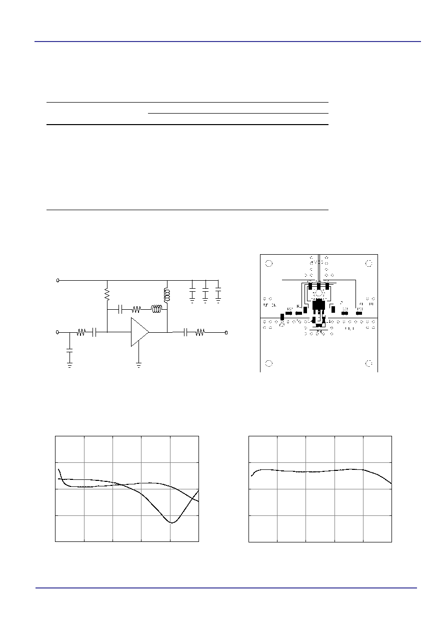
Application Circuit: 900 MHz
Typical Performance
Board Layout (FR4, 40x40 mm
2
, 0.8T)
Gain vs. Temperature
Frequency 900
MHz
Magnitude S21
18 dB
Magnitude S11
1)
-24
dB
Magnitude S22
1)
-11
dB
Output P1dB
24 dBm
Output IP3
2)
41
dBm
Noise Figure
2.6 dB
Supply Voltage
6 V
Current 110
mA
Schematic
S-parameters
6
0
0
7
0
0
8
0
0
9
0
0
1
0
0
0
1
1
0
0
1
2
0
0
-4
0
-3
5
-3
0
-2
5
-2
0
-1
5
85
o
C
25
o
C
-4
0
o
C
S1
2
[
d
B]
F
r
equenc y [MHz ]
50
C2=8 pF
C1=10 pF
R1=7.5 k
L1=100 nH
C3=100 pF
Vcc=6 V
RF IN
RF OUT
3 mm
ASG304
C4=
100 pF
C5=
1000 pF
C6=
0.1
�F
600
700
800
900
1000
1100
1200
-50
-40
-30
-20
-10
0
10
85
o
C
25
o
C
-40
o
C
S1
1 (
d
B
)
Frequency (MHz)
600
700
800
900
1000
1100
1200
-40
-35
-30
-25
-20
-15
85
o
C
25
o
C
-40
o
C
S12 (
d
B)
Frequency (MHz)
600
700
800
900
1000
1100
1200
0
5
10
15
20
25
85
o
C
25
o
C
-40
o
C
S2
1 (
d
B
)
Frequency (MHz)
600
700
800
900
1000
1100
1200
-20
-15
-10
-5
0
5
85
o
C
25
o
C
-40
o
C
S22 (
d
B)
Frequency (MHz)
-60
-40
-20
0
20
40
60
80
100
16
17
18
19
20
Frequency=900 MHz
Ga
i
n
(
d
B
)
Temperature (
o
C)

4/8 www.ASB.co.kr June 2003
800
825
850
875
900
925
950
20
25
30
35
40
45
50
55
60
85
o
C
25
o
C
-40
o
C
O
u
t
p
u
t
IP
3
(d
B
m
)
Frequency (MHz)
880 MHz Adjacent Channel Power vs. Channel Output Power
IS-95, 9 Channels Forward
P1dB vs. Frequency
Output IP3 vs. Frequency (Pout per tone = 8 dBm)
Output IP3 vs. Tone Power (Frequency = 900 MHz)
ASG304
800
825
850
875
900
925
950
20
22
24
26
28
30
85
o
C
25
o
C
-40
o
C
P1d
B
(
d
B
m
)
Frequency (MHz)
4
6
8
10
12
14
16
18
20
-85
-80
-75
-70
-65
-60
-55
-50
-45
-40
-35
-30
-25
-20
85
o
C
25
o
C
-40
o
C
A
d
j
acent
Ch
annel
Pow
e
r
(
d
Bc)
Channel Output Power (dBm)
8
9
10
11
12
13
14
15
16
20
25
30
35
40
45
50
55
60
85
o
C
25
o
C
-40
o
C
O
u
t
put
I
P
3
(
d
Bm)
P
out
per tone (dBm)

5/8 www.ASB.co.kr June 2003
1) S11 & S22 can be improved, at a specific frequency, by moving
an input shunt capacitor (C2) and inductor (L2) along an input transmission line.
2) OIP3 is measured with two tones at an output power of +8 dBm/tone
separated by 1 MHz.
Application Circuit: 2000 MHz
Typical Performance
S-parameters
Frequency 2000
MHz
Magnitude S21
10.5 dB
Magnitude S11
1)
-20
dB
Magnitude S22
1)
-15
dB
Output P1dB
24 dBm
Output IP3
2)
40
dBm
Noise Figure
3.5 dB
Supply Voltage
6 V
Current 110
mA
Schematic
ASG304
Board Layout (FR4, 40x40 mm
2
, 0.8T)
Gain vs. Temperature
ASG304
C1=10 pF
C2=2.7 pF
GND
L2=3.3 nH
5 mm
RF IN
50
C3=5 pF
RF OUT
8.75 mm
R1=7.5 k
L1=56 nH
Vcc=6 V
C5=
1000 pF
C4=
100 pF
C6=
0.1
�F
1800
1900
2000
2100
2200
-60
-40
-20
0
20
85
o
C
25
o
C
-40
o
C
S1
1 (
d
B)
Frequency (MHz)
1800
1900
2000
2100
2200
-30
-25
-20
-15
-10
85
o
C
25
o
C
-40
o
C
S12 (
d
B)
Frequency (MHz)
1800
1900
2000
2100
2200
0
5
10
15
20
85
o
C
25
o
C
-40
o
C
S2
1 (
d
B
)
Frequency (MHz)
1800
1900
2000
2100
2200
-30
-20
-10
0
10
85
o
C
25
o
C
-40
o
C
S2
2 (
d
B
)
Frequency (MHz)
-60
-40
-20
0
20
40
60
80
100
10
11
12
13
14
Frequency=2 GHz
Ga
i
n
(
d
B
)
Temperature (
o
C)

6/8 www.ASB.co.kr June 2003
1960 MHz Adjacent Channel Power vs. Channel Output Power
IS-95, 9 Channels Forward
P1dB vs. Frequency
Output IP3 vs. Frequency (Pout per tone = 8 dBm)
Output IP3 vs. Tone Power (Frequency = 2 GHz)
1800
1900
2000
2100
20
22
24
26
28
30
85
o
C
25
o
C
-40
o
C
P1
d
B
(
d
Bm)
Frequency (MHz)
1800
1900
2000
2100
20
25
30
35
40
45
50
55
60
85
o
C
25
o
C
-40
o
C
O
u
t
p
u
t
IP
3
(d
B
m
)
Frequency (MHz)
4
6
8
10
12
14
16
18
20
-85
-80
-75
-70
-65
-60
-55
-50
-45
-40
-35
-30
-25
-20
85
o
C
25
o
C
-40
o
C
A
d
jacen
t
Ch
an
nel
Po
w
e
r
(
d
Bc)
Channel Output Power (dBm)
ASG304
8
10
12
14
16
20
25
30
35
40
45
50
55
60
85
o
C
25
o
C
-40
o
C
Ou
t
put
I
P
3
(
d
Bm
)
P
out
per tone (dBm)
7/8 www.ASB.co.kr June 2003
* Zo=50
, Vcc=6 V, Ic=120 mA
Frequency (MHz)
Parameters
Units
50 250 450 650 850
Gain
dB 13.3 13.4 13.2 13.6 13.1
Output
P1dB dBm 22 23 22.4 22 21.5
S11 dB
-8.1
-8.2
-9.1
-12
-15.8
S22
dB -8.4 -9.5 -9.2 -8.8 -10.1
S12
dB -43 -41 -37 -33 -30
Noise
Figure dB 5.2 5.4 5.9 5.9 5.6
OIP3 dBm
36 38 37 33 35
OIP2 dBm
49 52 53 63 70
Application Circuit: 50-860 MHz for CATV
Typical Performance
S-parameters
Schematic
Board Layout (FR4, 40x40 mm
2
, 0.8T)
ASG304
C2=3.3 pF
C1=1000 pF
R1=7.5 k
L2=100 nH
C3=1000 pF
Vcc=6 V
RF IN
RF OUT
ASG304
C5=
100 pF
C6=
1000 pF
C7=
0.1
�F
R2=20
R4=270
R3=20
C4=1000 pF
L1=39 nH
0
200
400
600
800
1000
0
5
10
15
20
S21
(
d
B
)
Frequency (MHz)
0
200
400
600
800
1000
-20
-15
-10
-5
0
S22
S11
S11
an
d
S22
(
d
B
)
Frequency (MHz)

8/8 www.ASB.co.kr June 2003
1) OIP3 is measured with two tones at an output power of +8 dBm/tone
separated by 1 MHz.
2) For 6 V operation, R
Bias
should be replaced with 7.5 kohm
.
OIP vs. Frequency
Noise Figure vs. Frequency
ASG304
Frequency (MHz)
100
100
Magnitude S21 (dB)
19.6
19.7
Magnitude S11 (dB)
-13.5
-13.5
Magnitude S22 (dB)
-11.0
-11.0
Output P1dB (dBm)
22.0
22.8
Output IP3
1)
(dBm)
37
36
Noise Figure (dB)
5.6
5.6
Supply Voltage (V)
5
6
2)
Current (mA)
113
114
Typical Performance
Board Layout (FR4, 40x40 mm
2
, 0.8T)
Schematic
S-parameters
Application Circuit: 10-200 MHz for IF
C2=100 pF
C1=68 nF
R
BIAS
=6.2 k
L1=560 nH
ASG304
C3=68 nF
C4=
100 pF
C5=
1000 pF
C6=
0.1
�F
Vcc=5 V
RF IN
RF OUT
R1=30
R3=20
R2=750
0
50
100
150
200
0
10
20
30
40
Gain
G
a
in
(
d
B
)
Frequency (MHz)
0
200
400
600
800
1000
0
2
4
6
8
10
N
o
i
se Fi
gur
e (
d
B
)
Frequency (MHz)
0
50
100
150
200
-20
-15
-10
-5
0
S11
S22
S
1
1 an
d
S
22 (
d
B)
Frequency (MHz)
0
200
400
600
800
1000
10
20
30
40
50
60
70
80
OIP3
OIP2
OI
P2
an
d
OI
P
3
(
d
B
m
)
Frequency (MHz)