 | –≠–ª–µ–∫—Ç—Ä–æ–Ω–Ω—ã–π –∫–æ–º–ø–æ–Ω–µ–Ω—Ç: EC4558 | –°–∫–∞—á–∞—Ç—å:  PDF PDF  ZIP ZIP |

August 2003
Rev.1.0
General Description
The EC4558 consists of two high performance opera-
tional amplifiers. The IC features high gain, high input
resistance, excellent channel separation, wide range of
operating voltage and internal frequency compensa-
tion. It is specifically suitable for applications in differ-
ential-in, differential-out as well as in potential-metric
amplifiers and where gain and phase matched channels
are mandatory. The EC4558 contains
18Vmaximum
power supply voltage.
The EC4558 is available in DIP-8 or SOIC-8 package.
Features
Internal frequency compensation
Large DC voltage gain with 100 dB typical
High input resistance with 5M typical
Low input noise voltage with 10nV/
Maximum power supply voltages: 18V
Compatible with NJM 4558
Applications
Audio AC-3 decoded system
Audio amplifier
Pin Configuration
DIP-8
SOIC-8
Functional Block Diagram
Figure 2. Pin Configuration of
EC
4558
Figure 3. Representative Schematic Diagram of
EC
4558 (Each amplifier)
HZ
SOIC-8/DIP-8
Top View
Figure 1. Package Types of
EC
4558
8 V
CC
7 OUTPUT 2
6 INPUT 2-
5 INPUT 2+
1
2
3
4
OUTPUT 1
INPUT 1-
INPUT 1+
V
EE
Dual Channel Operational Amplifiers
EC
4558
August 2003
Rev.1.0
Recommended Operating Conditions
Parameter Symbol
Value
Unit
Power Supply Voltage
V
CC
+ 18
V
V
EE
- 18
Differential Input Voltage
V
ID
± 30
V
Input Voltage
V
IC
± 15
V
Power Dissipation
P
D
DIP
500
mW
SOIC
800
Operating Temperature Range
T
OP
-40 to 85
o
C
Storage Temperature Range
T
STG
-40 to 125
o
C
Parameter
Min
Max
Unit
Supply Voltage
± 4
± 18
V
Absolute Maximum Ratings (Note 1)
Package
Temperature Range
Part Number
Marking ID
Packing Type
SOIC-8
-40 to 85
o
C
EC4558M
4558M
Tube/Tape/Reel
DIP-8
EC4558P
EC4558P
Tube
Ordering Information
Note 1: Stresses greater than those listed under "Absolute Maximum Ratings" may cause permanent damage to the
device. These are stress ratings only, and functional operation of the device at these or any other conditions beyond
those indicated under "Recommended Operating Conditions" is not implied. Exposure to "Absolute Maximum
Ratings" for extended periods may affect device reliability.
EC 4558 Y
Circuit Type
Package
P: DIP-8
M: SOIC-8
Dual Channel Operational Amplifiers
EC
4558

August 2003
Rev.1.0
Operating Conditions: V
CC
=
+
15V, V
EE
= - 15V, T
A
= 25
o
C unless otherwise specified.
Electrical Characteristics
Parameter
Conditions
Min
Typ
Max
Unit
Input Offset Voltage
-
0.5
6
mV
Input Bias Current
V
CM
= 0V
-
25
250
nA
Input Offset Current
V
CM
= 0V
-
2.5
100
nA
Input Resistance
0.3
5
-
M
Supply Current
R
L
=
, Over full temperature
range
-
3.3
5.7
mA
Large Signal Voltage Gain
R
L
2,
V
O
= 1V to 11V
85
100
-
dB
Common Mode Rejection Ratio
V
CM
= 0V to V
CC
- 15V
80
92
-
dB
Power Supply Rejection Ratio
V
CC
=5V to 18V
V
EE
=
-
5V to - 18V
80
95
-
dB
Output Current
Source
V+ = 1V, V- = 0V
-
50
-
mA
Sink
V+ = 0V, V- = 1V
-
50
-
mA
Output Voltage Swing
R
L
2K
±
10
±
13
-
V
R
L
10K
±
12
±
14
-
Slew Rate
-
1.3
-
V /
µ
S
Equivalent Input Noise Voltage
Rs=50
, f=1KHz
-
10
-
nV/(HZ)
0.5
Gain Bandwidth Product
-
3.4
-
MHz

August 2003
Rev.1.0
Figure 4. Open Loop Voltage Gain vs. Frequency
Figure 5. Maximum Output Voltage Swing vs. Frequency
Figure 6. Maximum Output Voltage Swing
Figure 7. Equivalent Input Noise Voltage vs. Frequency
vs. Load Resistance
2x10
0
HZ 10
1
HZ
10
2
HZ
10
3
HZ
10
4
HZ
10
5
HZ
10
6
HZ
0
20
40
60
80
100
120
V
CC
=15V, V
EE
=-15V
R
L
=2K,T
A
=25
o
C
O
pen Loop V
o
lt
ag
e
G
a
in
(dB)
Frequency (HZ)
0.1K
1K
10K
12
14
16
18
20
22
24
26
28
30
V
CC
=15V,V
EE
=-15V,T
A
=25
o
C
O
utpu
t
V
olt
age Swi
ng
(V
)
Load Resistance (k
)
10
0
HZ
10
1
HZ
10
2
HZ
10
3
HZ
10
0
10
1
10
2
10
3
Frequency (HZ)
E
quivllent
Inp
ut Nois
e V
olt
age (nV
/
(HZ)
0.
5
)
V
CC
=15V, V
EE
=-15V
R
S
=50
,T
A
=25
o
C
10
1
HZ
10
2
HZ
10
3
HZ
10
4
HZ
10
5
HZ
10
6
HZ
0
5
10
15
20
25
30
O
utput Voltage Swi
ng (V)
Frequency (HZ)
V
CC
=15V,V
EE
=-15V,
R
L
=2K, T
A
=25
o
C
Typical Performance Characteristics
Dual Channel Operational Amplifiers
EC
4558

August 2003
Rev.1.0
Figure 8. Input Offset Voltage vs. Temperature
Figure 9. Input Bias Current vs. Temperature
Typical Application
Figure 10. Typical Application of
EC
4558
-25
0
25
50
75
100
125
0
10
20
30
40
50
60
70
80
V
CC
=15V
V
EE
=-15V
B
i
a
s
Cu
rr
en
t
(n
A)
Ambient Temperature (
o
C)
-25
0
25
50
75
100
125
0.2
0.3
0.4
0.5
0.6
0.7
0.8
0.9
1.0
1.1
1.2
V
CC
=15V
V
EE
=-15V
Of
f
s
e
t
Vo
l
t
a
g
e
(m
V)
Ambient Temperature (
o
C)
Typical Performance Characteristics (Continued)
D2
D1
8
7
6
5
1
2
3
4
15K
20K
20K
10K
V
IN
V
O
10
µF
20K
6.2K
20K
-
+
-
+
EC
4558
Dual Channel Operational Amplifiers
EC
4558
August 2003
Rev.1.0
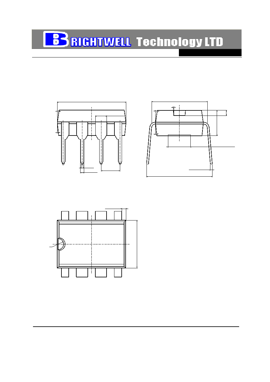
Mechanical Dimensions
DIP - 8
4∞
6∞
R0.75
0
.
7
3◊0.15±0.05
6
.
6
0
±
0
.
5
0
0.457
0.254
0.13MIN
2.54
10.0MAX
0.28±0.07
1.46±0.31
7.62±0.25
4∞
6∞
5∞
3
.
3
0
±
0
.
3
0
9.2±0.10
Unit: mm
Dual Channel Operational Amplifiers
EC
4558

August 2003
Rev.1.0
SOIC - 8
Mechanical Dimensions (Continued)
8∞
D
±4∞
4∞
3∞
±2∞
R0.15
R0.15
1.00
0.42±0.09
4.9±0.10
1
.
5
5
±
0
.
2
0
0
.
2
±
0
.
1
0
0
.
9
0
0.8
6.00±0.20
0
.
2
2
±
0
.
0
3
0
.
7
0
±
0
.
0
2
5
0.32
0
.
2
0
3
.
9
0
±
0
.
1
0
7∞
7∞
8∞
20:1
D
Unit: mm
Dual Channel Operational Amplifiers
EC
4558