Specifications and information are subject to change without notice
WJ Communications, Inc
Phone 1-800-WJ1-4401
FAX: 408-577-6621
e-mail: sales@wj.com
Web site: www.wj.com
December 2004 Rev 1
ECG006
InGaP HBT Gain Block
Product Information
The Communications Edge
TM
Product Features
x
DC � 5.5 GHz
x
+15.5 dBm P1dB at 1 GHz
x
+32 dBm OIP3 at 1 GHz
x
15 dB Gain at 1 GHz
x
4.0 dB Noise Figure at 2 GHz
x
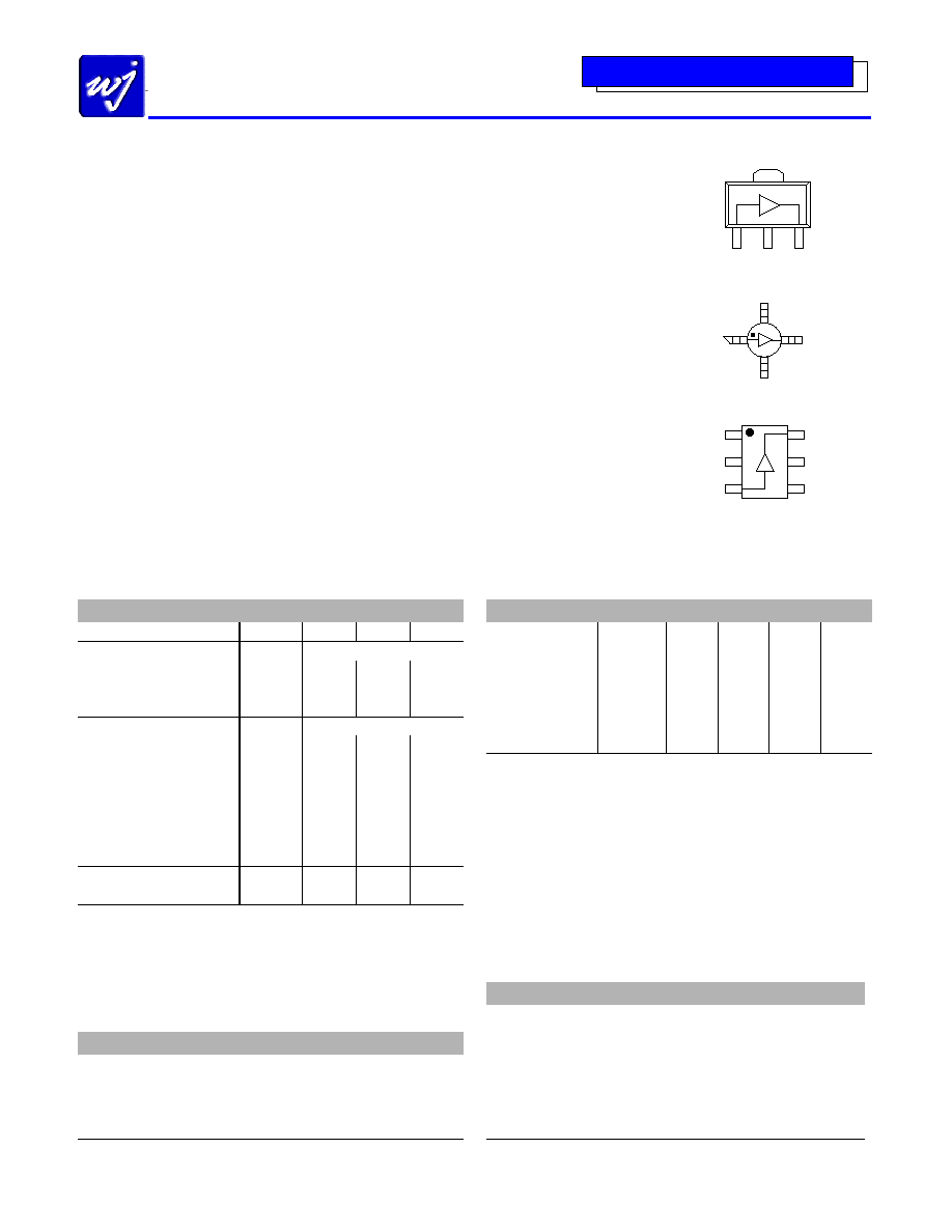
Available in SOT-363, SOT-86,
and lead-free / green SOT-89
Package Styles
x
Internally matched to 50
:
Applications
x
Mobile Infrastructure
x
CATV / DBS
x
W-LAN / ISM
x
RFID
x
Defense / Homeland Security
x
Fixed Wireless
Product Description
The ECG006 is a general-purpose buffer amplifier that
offers high dynamic range in a low-cost surface-mount
package. At 1000 MHz, the ECG006 typically provides 15
dB of gain, +32 dBm Output IP3, and +15.5 dBm P1dB.
The ECG006 consists of Darlington pair amplifiers using
the high reliability InGaP/GaAs HBT process technology
and only requires DC-blocking capacitors, a bias resistor,
and an inductive RF choke for operation. The device is
ideal for wireless applications and is available in low-cost,
surface-mountable plastic SOT-86, SOT-363, and SOT-89
packages. The ECG006 is also available in a lead-
free/green/RoHS-compliant SOT-89 package. All devices
are 100% RF and DC tested.
The broadband MMIC amplifier can be directly applied to
various current and next generation wireless technologies
such as GPRS, GSM, CDMA, and W-CDMA. In addition,
the ECG006 will work for other various applications within
the DC to 5.5 GHz frequency range such as CATV and
fixed wireless.
Functional Diagram
RF IN
GND
RF OUT
GND
1
2
3
4
ECG006B / ECG006B-G
RF Out
RF In
GND
GND
1
2
3
4
ECG006C
RF IN
GND
RF OUT
GND
GND
GND 1
2
3
4
6
5
ECG006F
Specifications
(1)
Parameter
Units Min Typ Max
Operational Bandwidth
MHz
DC
5500
Test Frequency
MHz
1000
Gain
dB
15
Output P1dB
dBm
+15.4
Output IP3
(2)
dBm
+32
Test Frequency
MHz
2000
Gain
dB
14
Large-signal Gain
(3)
dB
11.5
13
Input Return Loss
dB
18
Output Return Loss
dB
14
Output P1dB
dBm
15.0
Output IP3
(2)
dBm
32
Noise Figure
dB
4.0
Device Voltage
V
3.5
3.9
4.3
Device Current
mA
45
1. Test conditions unless otherwise noted: 25� C, Supply Voltage = +5 V, Rbias = 24.3
�
, 50
�
System.
2. 3OIP measured with two tones at an output power of +2 dBm/tone separated by 1 MHz. The
suppression on the largest IM3 product is used to calculate the 3OIP using a 2:1 rule.
3. Large-signal gain is tested with an input power level of +2 dBm.
Absolute Maximum Rating
Parameter
Rating
Operating Case Temperature
-40 to +85
qC
Storage Temperature
-55 to +150
qC
Device Current
150 mA
RF Input Power (continuous)
+12 dBm
Junction Temperature
+250
qC
Operation of this device above any of these parameters may cause permanent damage.
Typical Performance
(4)
Parameter
Units
Typical
Frequency
MHz
500
900
1900
2140
S21
dB
15.5
15
14.2
14
S11
dB
-20
-14
-17.4
-18
S22
dB
-16
-13
-14.5
-15
Output P1dB
dBm
+15.8 +15.4
+15
+15
Output IP3
(2)
dBm
+32
+32
+30
+30
Noise Figure
dB
3.7
3.7
3.7
3.7
4. Test conditions: T = 25� C, Supply Voltage = +5 V, Device Voltage = +3.9V, R
bias
= 24.3
�
, 50
�
System.
Ordering Information
Part No.
Description
ECG006B
InGaP HBT Gain Block
(leaded SOT-89 Pkg)
ECG006B-G
InGaP HBT Gain Block
(lead-free/green/RoHS-compliant SOT-89 Pkg)
ECG006C
InGaP HBT Gain Block (SOT-86 Pkg)
ECG006F
InGaP HBT Gain Block (SOT-363 Pkg)
ECG006B-PCB
700 � 2400 MHz Fully Assembled Eval. Board
ECG006C-PCB
700 � 2400 MHz Fully Assembled Eval. Board
ECG006F-PCB
700 � 2400 MHz Fully Assembled Eval. Board
Specifications and information are subject to change without notice
WJ Communications, Inc
Phone 1-800-WJ1-4401
FAX: 408-577-6621
e-mail: sales@wj.com
Web site: www.wj.com
December 2004 Rev 1
ECG006
InGaP HBT Gain Block
Product Information
The Communications Edge
TM
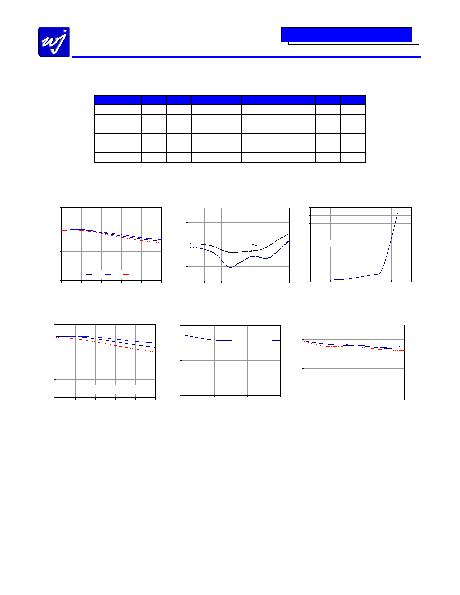
Typical Device RF Performance
Supply Bias = +5 V, R
bias
= 24.3
:, I
cc
= 45 mA
Frequency
MHz
100
500
900
1900
2140
2400
3500
5800
S21
dB
15.3
15.2
15.1
14.5
14.3
14.1
13.9
10.2
S11
dB
-20
-18
-14
-17
-18
-20
-17
-12.5
S22
dB
-29
-16
-13
-14
-14
-15
-15
-9.5
Output P1dB
dBm
+15.8 +15.4 +15.2 +15.0 +14.9 +14.6
+14
Output IP3
dBm
+31
+31.5
+32
+30
+30
+29.6
Noise Figure
dB
3.8
3.7
3.6
3.6
3.6
3.6
1. Test conditions: T = 25� C, Supply Voltage = +5 V, Device Voltage = +3.9 V, Rbias = 24.3
�
, Icc = 45 mA typical, 50
�
System.
2. 3OIP measured with two tones at an output power of +2 dBm/tone separated by 1 MHz. The suppression on the largest IM3 product is used to calculate the 3OIP using a 2:1 rule.
3. Data is shown as device performance only. Actual implementation for the desired frequency band will be determined by external components shown in the application circuit.
Gain vs. Frequency
8
10
12
14
16
18
500
1000
1500
2000
2500
3000
Frequency (MHz)
G
a
i
n
+25C
-40C
+85C
S11, S22 vs. Frequency
-25
-20
-15
-10
-5
0
0
1
2
3
4
5
6
Frequency (GHz)
S
1
1
,
S
2
2
(
d
B
)
S22
S11
Vde vs. Icc
0
10
20
30
40
50
60
70
80
90
0.0
1.0
2.0
3.0
4.0
5.0
Vde (V)
I
c
c
(
m
A
)
+25�C
OIP3 vs. Frequency
15
20
25
30
35
500
1000
1500
2000
2500
3000
Frequency (MHz)
O
I
P
3
(
d
B
m
)
+25�C
-40�C
+85�C
Noise Figure vs. Frequency
2
2.5
3
3.5
4
500
1000
1500
2000
Frequency (MHz)
N
F
(
d
B
)
P1dB vs. Frequency
8
10
12
14
16
18
500
1000
1500
2000
2500
3000
Frequency (MHz)
P
1
d
B
(
d
B
m
)
+25�C
-40�C
+85�C
Specifications and information are subject to change without notice
WJ Communications, Inc
Phone 1-800-WJ1-4401
FAX: 408-577-6621
e-mail: sales@wj.com
Web site: www.wj.com
December 2004 Rev 1
ECG006
InGaP HBT Gain Block
Product Information
The Communications Edge
TM
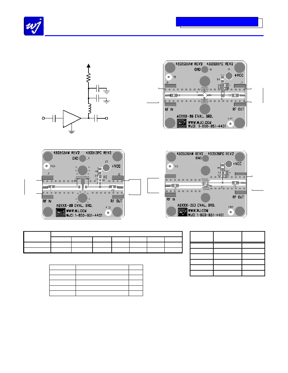
Recommended Application Circuit
ECG006B-PCB
ECG006C-PCB
ECG006F-PCB
Recommended Component Values
Reference
Frequency (MHz)
Designator
50
500
900
1900
2200
2500
3500
L1
820 nH
220 nH
68 nH
27 nH
22 nH
18 nH
15 nH
C1, C2, C4
.018 �F
1000 pF
100 pF
68 pF
68 pF
56 pF
39 pF
1. The proper values for the components are dependent upon the intended frequency of operation.
2. The following values are contained on the evaluation board to achieve optimal broadband performance:
Ref. Desig.
Value / Type
Size
L1
39 nH wirewound inductor
0603
C1, C2
56 pF chip capacitor
0603
C3
0.018
PF chip capacitor
0603
C4
Do Not Place
R4
24.3
: 1% tolerance
0805
Recommended Bias Resistor Values
Supply
Voltage
R1 value
Size
5 V
24.4 ohms
0805
6 V
46.7 ohms
0805
8 V
91 ohms
1210
9 V
113 ohms
1210
10 V
136 ohms
2010
12 V
180 ohms
2010
The proper value for R1 is dependent upon the supply
voltage and allows for bias stability over temperature.
WJ recommends a minimum supply bias of +5 V.
A
1% tolerance resistor is recommended.
C1
Blocking
Capacitor
RF OUT
L1
RF Choke
C3
0.018 �F
R4
Bias
Resistor
RF IN
C4
Bypass
Capacitor
C2
Blocking
Capacitor
Vcc
Icc = 45 mA
ECG006
Specifications and information are subject to change without notice
WJ Communications, Inc
Phone 1-800-WJ1-4401
FAX: 408-577-6621
e-mail: sales@wj.com
Web site: www.wj.com
December 2004 Rev 1
ECG006
InGaP HBT Gain Block
Product Information
The Communications Edge
TM
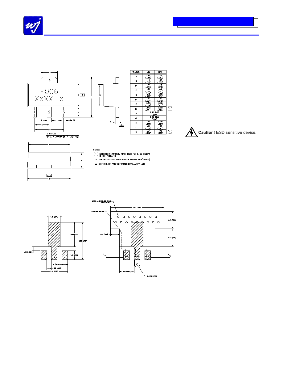
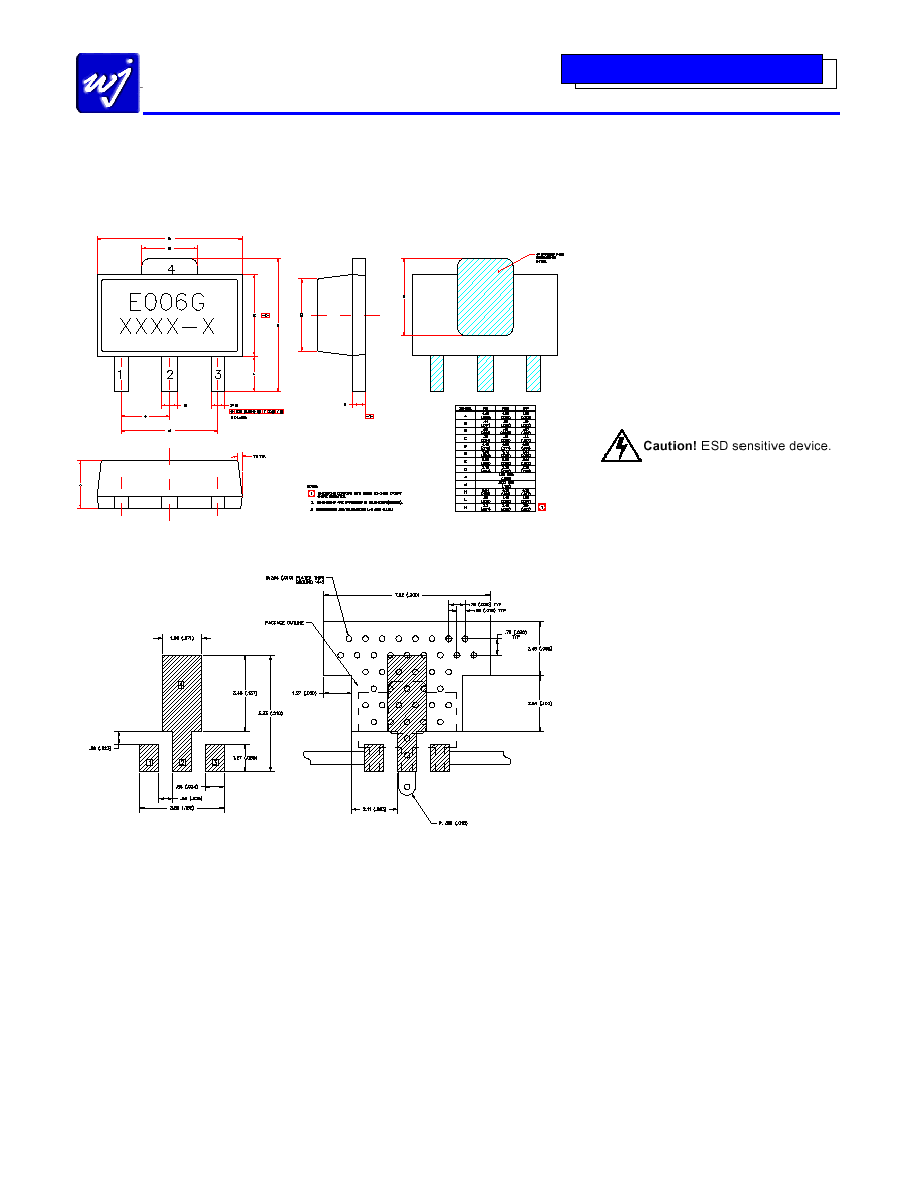
ECG006B (SOT-89 Package) Mechanical Information
This package may contain lead-bearing materials. The plating material on the leads is SnPb.
Outline Drawing
Land Pattern
Product Marking
The component will be marked with an
"E006" designator with an alphanumeric lot
code on the top surface of the package.
Tape and reel specifications for this part are
located on the website in the "Application
Notes" section.
MSL / ESD Rating
ESD Rating: Class 1A
Value:
Passes between 250 and 500V
Test:
Human Body Model (HBM)
Standard:
JEDEC Standard JESD22-A114
MSL Rating: Level 3 at +235
�
C convection reflow
Standard:
JEDEC Standard J-STD-020
Mounting Config. Notes
1. Ground / thermal vias are critical for the proper
performance of this device. Vias should use a .35mm
(#80 / .0135" ) diameter drill and have a final plated
thru diameter of .25 mm (.010" ).
2. Add as much copper as possible to inner and outer
layers near the part to ensure optimal thermal
performance.
3. Mounting screws can be added near the part to fasten
the board to a heatsink. Ensure that the ground /
thermal via region contacts the heatsink.
4. Do not put solder mask on the backside of the PC board
in the region where the board contacts the heatsink.
5. RF trace width depends upon the PC board material
and construction.
6. Use 1 oz. Copper minimum.
7. All dimensions are in millimeters (inches). Angles are
in degrees.
Specifications and information are subject to change without notice
WJ Communications, Inc
�
Phone 1-800-WJ1-4401
�
FAX: 408-577-6621
�
e-mail: sales@wj.com
�
Web site: www.wj.com
December 2004 Rev 1
ECG006
InGaP HBT Gain Block
Product Information
The Communications Edge
TM
ECG006B-G (Green / Lead-free SOT-89 Package) Mechanical Information
This package is lead-free/Green/RoHS-compliant. It is compatible with both lead-free (maximum 260
qC reflow temperature) and leaded
(maximum 245
qC reflow temperature) soldering processes. The plating material on the leads is NiPdAu.
Outline Drawing
Land Pattern
Product Marking
The component will be marked with an
" E006G" designator with an alphanumeric lot
code on the top surface of the package.
Tape and reel specifications for this part are
located on the website in the " Application
Notes" section.
MSL / ESD Rating
ESD Rating: Class 1A
Value:
Passes between 250 and 500V
Test:
Human Body Model (HBM)
Standard:
JEDEC Standard JESD22-A114
MSL Rating: Level 3 at +260
�
C convection reflow
Standard:
JEDEC Standard J-STD-020
Mounting Config. Notes
1. Ground / thermal vias are critical for the proper
performance of this device. Vias should use a .35mm
(#80 / .0135" ) diameter drill and have a final plated
thru diameter of .25 mm (.010" ).
2. Add as much copper as possible to inner and outer
layers near the part to ensure optimal thermal
performance.
3. Mounting screws can be added near the part to fasten
the board to a heatsink. Ensure that the ground /
thermal via region contacts the heatsink.
4. Do not put solder mask on the backside of the PC board
in the region where the board contacts the heatsink.
5. RF trace width depends upon the PC board material
and construction.
6. Use 1 oz. Copper minimum.
7. All dimensions are in millimeters (inches). Angles are
in degrees.
Specifications and information are subject to change without notice
WJ Communications, Inc
�
Phone 1-800-WJ1-4401
�
FAX: 408-577-6621
�
e-mail: sales@wj.com
�
Web site: www.wj.com
December 2004 Rev 1
ECG006
InGaP HBT Gain Block
Product Information
The Communications Edge
TM
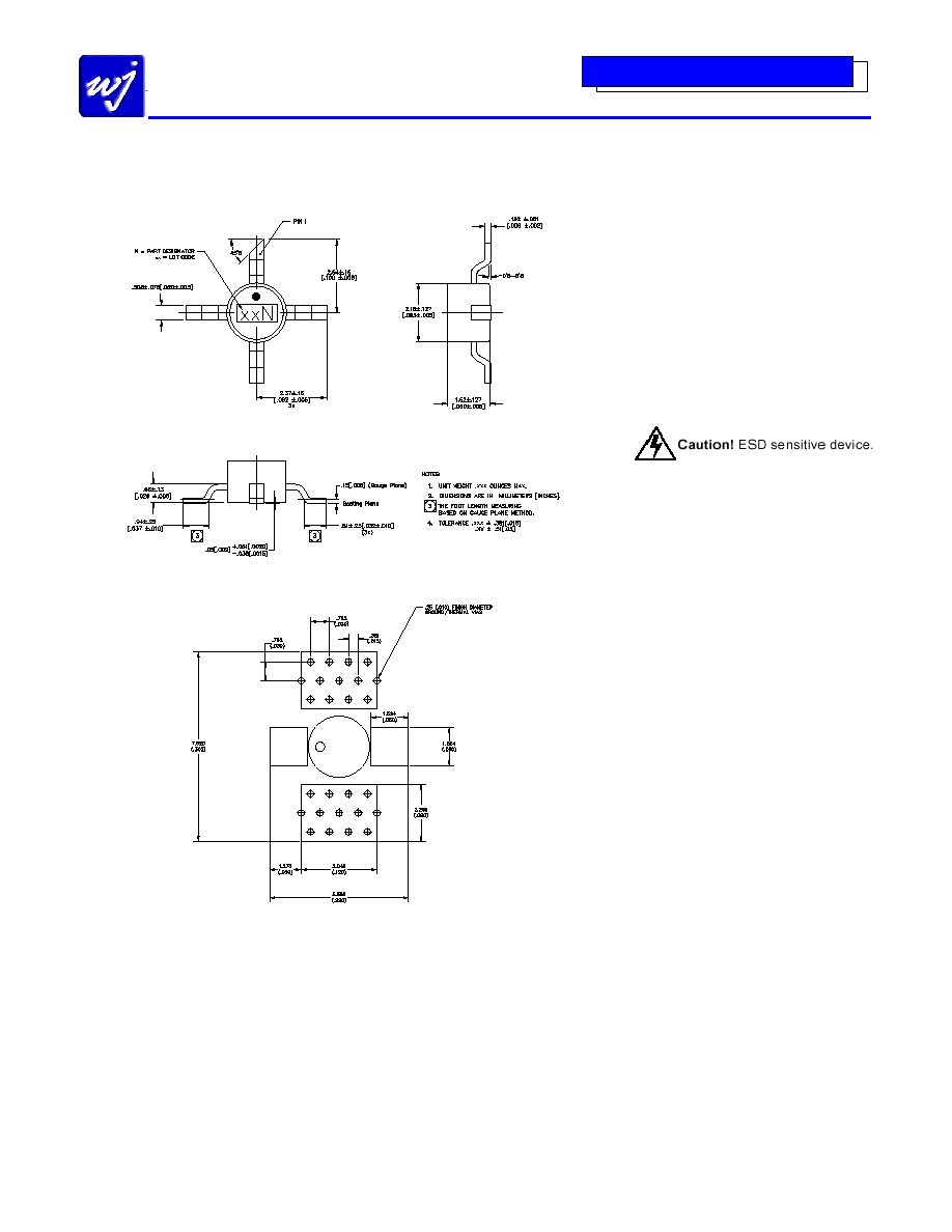
ECG006C (SOT-86 Package) Mechanical Information
Outline Drawing
Land Pattern
Product Marking
The component will be marked with a two-
digit numeric lot code followed by an " N"
designator on the top surface of the
package.
Tape and reel specifications for this part are
located on the website in the " Application
Notes" section.
MSL / ESD Rating
ESD Rating: Class 1A
Value:
Passes between 250 and 500V
Test:
Human Body Model (HBM)
Standard:
JEDEC Standard JESD22-A114
MSL Rating: Level 1 at +235
�
C convection reflow
Standard:
JEDEC Standard J-STD-020
Mounting Config. Notes
1. Ground / thermal vias are critical for the proper
performance of this device. Vias should use
a .35mm (#80 / .0135" ) diameter drill and have a
final plated thru diameter of .25 mm (.010" ).
2. Add as much copper as possible to inner and outer
layers near the part to ensure optimal thermal
performance.
3. Mounting screws can be added near the part to fasten
the board to a heatsink. Ensure that the ground /
thermal via region contacts the heatsink.
4. Do not put solder mask on the backside of the PC
board in the region where the board contacts the
heatsink.
5. RF trace width depends upon the PC board material
and construction.
6. Use 1 oz. Copper minimum.
7. All dimensions are in millimeters (inches). Angles
are in degrees.
Specifications and information are subject to change without notice
WJ Communications, Inc
�
Phone 1-800-WJ1-4401
�
FAX: 408-577-6621
�
e-mail: sales@wj.com
�
Web site: www.wj.com
December 2004 Rev 1
ECG006
InGaP HBT Gain Block
Product Information
The Communications Edge
TM
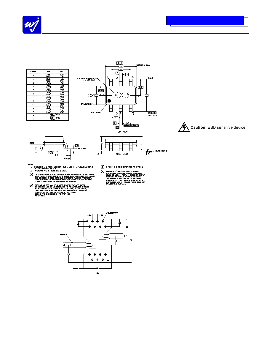
ECG006F (SOT-363 Package) Mechanical Information
Outline Drawing
Land Pattern
Product Marking
The component will be marked with a two-
digit numeric lot code (shown as " XX" )
followed with a " 3" designator on the top
surface of the package.
Tape and reel specifications for this part are
located on the website in the " Application
Notes" section.
MSL / ESD Rating
ESD Rating: Class 1A
Value:
Passes between 250 and 500V
Test:
Human Body Model (HBM)
Standard:
JEDEC Standard JESD22-A114
MSL Rating: Level 3 at +235
�
C convection reflow
Standard:
JEDEC Standard J-STD-020
Mounting Config. Notes
1. Ground / thermal vias are critical for the proper
performance of this device. Vias should use a .35mm
(#80 / .0135" ) diameter drill and have a final plated
thru diameter of .25 mm (.010" ).
2. Add as much copper as possible to inner and outer
layers near the part to ensure optimal thermal
performance.
3. Mounting screws can be added near the part to fasten
the board to a heatsink. Ensure that the ground /
thermal via region contacts the heatsink.
4. Do not put solder mask on the backside of the PC board
in the region where the board contacts the heatsink.
5. RF trace width depends upon the PC board material
and construction.
6. Use 1 oz. Copper minimum.
7. All dimensions are in millimeters (inches). Angles are
in degrees.

Specifications and information are subject to change without notice
WJ Communications, Inc
�
Phone 1-800-WJ1-4401
�
FAX: 408-577-6621
�
e-mail: sales@wj.com
�
Web site: www.wj.com
December 2004 Rev 1
ECG006
InGaP HBT Gain Block
Product Information
The Communications Edge
TM
Typical Device S-Parameters � ECG006B / ECG006B-G
S-Parameters (V
device
= +3.9 V, I
CC
= 45 mA, T = 25
�
C, calibrated to device leads)
Freq (MHz)
S11 (dB)
S11 (ang)
S21 (dB)
S21 (ang)
S12 (dB)
S12 (ang)
S22 (dB)
S22 (ang)
50
-16.18
-2.18
15.76
178.02
-18.89
-0.38
-14.36
-2.29
500
-16.13
-22.13
15.57
160.12
-18.77
-2.87
-14.40
-26.41
1000
-15.97
-44.58
15.21
141.76
-18.46
-5.33
-14.15
-51.57
1500
-15.79
-68.38
14.80
124.56
-17.94
-9.45
-13.78
-77.30
2000
-15.34
-96.24
14.57
108.50
-17.29
-14.37
-13.23
-104.15
2500
-14.99
-124.42
14.34
91.11
-16.69
-21.48
-12.79
-131.75
3000
-14.73
-153.90
14.02
74.20
-16.16
-29.16
-12.22
-160.58
3500
-14.29
174.59
13.65
56.77
-15.76
-38.37
-11.63
170.65
4000
-13.38
141.41
13.22
39.56
-15.49
-47.75
-10.44
143.61
4500
-11.80
110.87
12.66
22.19
-15.29
-57.59
-9.04
117.68
5000
-9.66
85.53
12.00
5.48
-15.28
-68.56
-7.50
96.34
5500
-7.85
63.77
11.20
-10.89
-15.43
-79.10
-6.12
76.71
6000
-6.37
47.01
10.36
-26.75
-15.69
-89.87
-4.95
59.58
Typical Device S-Parameters � ECG006C
S-Parameters (V
device
= +3.9 V, I
CC
= 45 mA, T = 25
�
C, calibrated to device leads)
Freq (MHz)
S11 (dB)
S11 (ang)
S21 (dB)
S21 (ang)
S12 (dB)
S12 (ang)
S22 (dB)
S22 (ang)
50
-13.66
-1.22
15.30
178.47
-18.67
-0.33
-12.25
-1.92
500
-13.64
-13.39
15.23
164.32
-18.59
0.29
-12.33
-20.62
1000
-14.11
-23.99
15.01
149.00
-18.38
0.78
-12.52
-41.41
1500
-15.20
-35.45
14.72
134.06
-17.99
0.29
-13.08
-62.51
2000
-17.86
-52.47
14.44
119.89
-17.52
-0.93
-14.31
-82.78
2500
-20.46
-93.43
14.06
105.18
-17.12
-3.33
-15.20
-99.71
3000
-18.86
-135.97
13.53
91.27
-16.59
-6.24
-15.01
-124.98
3500
-17.20
-158.47
12.99
77.75
-16.21
-10.91
-14.89
-157.99
4000
-16.45
-171.80
12.38
65.03
-15.93
-15.16
-14.50
170.24
4500
-17.31
166.84
11.76
52.68
-15.73
-19.74
-13.75
147.52
5000
-16.22
136.42
11.25
40.65
-15.52
-24.35
-12.08
133.59
5500
-13.68
110.91
10.56
28.09
-15.42
-29.98
-10.21
119.31
6000
-11.01
97.79
9.95
17.28
-15.43
-34.96
-8.73
106.39
Typical Device S-Parameters � ECG006F
S-Parameters (V
device
= +3.9 V, I
CC
= 45 mA, T = 25
�
C, calibrated to device leads)
Freq (MHz)
S11 (dB)
S11 (ang)
S21 (dB)
S21 (ang)
S12 (dB)
S12 (ang)
S22 (dB)
S22 (ang)
50
-16.22
-0.52
15.76
178.32
-18.82
-0.82
-14.16
-2.06
500
-14.87
-18.97
15.63
165.77
-18.87
1.49
-12.83
-24.91
1000
-16.45
-51.46
15.51
151.31
-18.40
1.44
-14.19
-55.98
1500
-16.41
-95.69
15.22
137.15
-18.07
0.35
-14.59
-93.37
2000
-14.08
-118.65
14.79
123.39
-17.74
-1.31
-13.52
-120.99
2500
-12.50
-114.48
14.48
112.93
-17.16
-2.57
-13.05
-122.53
3000
-12.18
-126.96
14.14
100.74
-16.80
-4.49
-12.19
-138.80
3500
-11.70
-139.53
13.94
88.52
-16.16
-8.66
-11.93
-159.41
4000
-10.97
-158.51
13.57
75.28
-15.72
-12.48
-11.00
174.63
4500
-10.24
178.62
13.03
62.14
-15.50
-19.07
-9.10
151.63
5000
-9.06
161.58
12.33
51.12
-15.19
-24.71
-7.50
139.14
5500
-8.32
150.77
11.60
42.08
-15.22
-28.00
-6.87
136.14
6000
-7.84
140.56
10.95
33.72
-15.14
-30.97
-6.78
137.51
Device S-parameters are available for download off of the website at: http://www.wj.com