Stock No. 23033-A
Advance Information - Subject to Change Without Notice
1
EM128L08
Advance Information
NanoAmp Solutions, Inc.
1982 Zanker Road, San Jose, CA 95112
ph: 408-573-8878, FAX: 408-573-8877
www.nanoamp.com
EM128L08 Family
128Kx8 Bit Ultra-Low Power Asynchronous Static RAM
Overview
The EM128L08 is an integrated memory device
containing a low power 1 Mbit Static Random
Access Memory organized as 131,072 words by 8
bits. The device is fabricated using NanoAmp's
advanced CMOS process and high-speed/low-
power circuit technology. This device is designed
for very low voltage operation making it quite suit-
able for battery powered devices. It is also
designed for both very low operating and standby-
currents. The device pinout is compatible with
other standard 128Kx8 SRAMs.
Features
�
Wide Voltage Range:
2.3 to 3.6 Volts
�
Extended Temperature Range:
-40 to +85
o
C
�
Fast Cycle Time:
T
ACC
< 55 ns @ 3.0V
�
Very Low Operating Current:
I
CC
< 10 mA typical at 3V, 10 Mhz
�
Very Low Standby Current:
I
SB
< 10
�
A
@ 55
o
C
�
32-Pin TSOP, STSOP, Packages Available
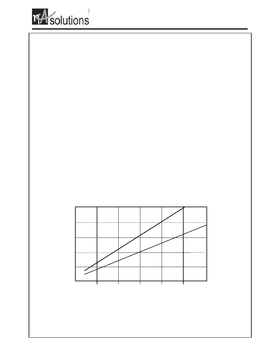
FIGURE 1: Typical Operating Current Curves
12.5
10.0
7.5
5.0
2.5
0.0
T
y
p
i
c
a
l
I
C
C
Operating Frequency (Mhz)
0 2.5 5.0 7.5 10.0 12.5 15.0
3.6 Volts
2.3 Volts
Stock No. 23033-A
Advance Information - Subject to Change Without Notice
2
EM128L08
NanoAmp Solutions, Inc.
Advance Information
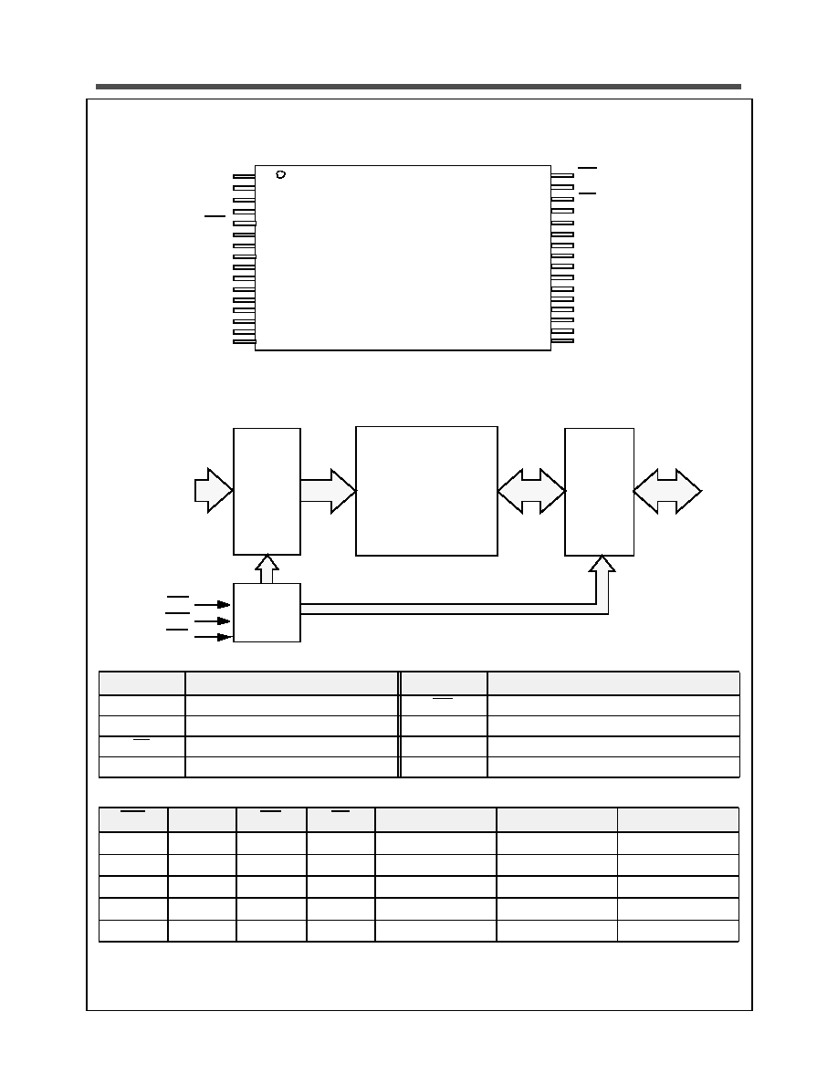
FIGURE 1: Pin Configuration
FIGURE 2: Functional Block Diagram
TABLE 1: Pin Description
TABLE 2: Functional Description
*The device will consume active power in this mode whenever addresses are changed
Pin Name
Pin Function
Pin Name
Pin Function
A0-A16
Address Inputs
WE
Write Enable (Active Low)
D0-D7
Data Inputs/Outputs
V
CC
Power
CE
Chip Enable (Active Low)
V
SS
Ground
OE
Output Enable (Active Low)
NC
Not Connected (Do not connect signal)
CE1
CE2
WE
OE
D0-D7
MODE
POWER
H
X
X
X
High Z
Standby
Standby
X
L
X
X
High Z
Standby
Standby
L
H
L
X
Data In
Write
Active -> Standby*
L
H
H
L
Data Out
Read
Active -> Standby*
L
H
H
H
High Z
Active
Standby*
EM128L08
STSOP, TSOP
2
3
4
5
1
6
7
8
9
10
11
12
13
14
15
16
23
18
17
22
21
20
19
27
26
25
24
31
30
29
28
32
A11
A9
A8
A13
WE
A15
VCC
NC
A16
A14
A12
A7
A6
A5
A4
A2
A10
CE
VSS
A3
A1
A0
D0
D1
D2
D3
D4
D5
D6
D7
O E
CE2
Control
Logic
128K x 8
RAM Array
Address
Decode
Logic
Address
Inputs
A
0
- A
16
CE
WE
OE
Input/
Output
Mux
and
Buffers
Data I/O
D
0
- D
7
Stock No. 23033-A
Advance Information - Subject to Change Without Notice
3
EM128L08
NanoAmp Solutions, Inc.
Advance Information
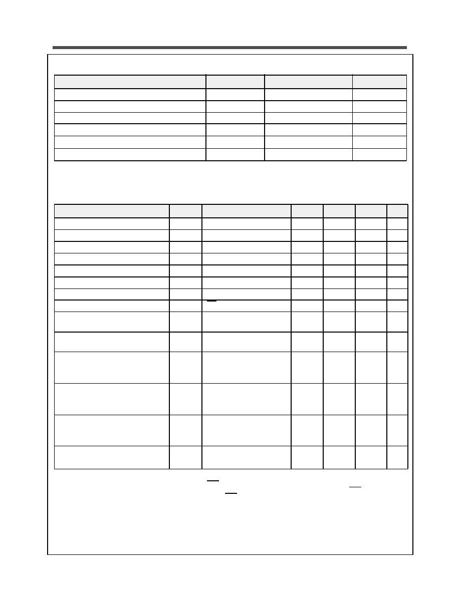
TABLE 3: Absolute Maximum Ratings*
* Stresses greater than those listed above may cause permanent damage to the device. This is a stress rating only and functional
operation of the device at these or any other conditions above those indicated in the operating section of this specification is not
implied. Exposure to absolute maximum rating conditions for extended periods may affect reliability.
TABLE 4: Operating Characteristics (Over specified Temperature Range)
Note 1. This device assumes a standby mode if either CE1 is disabled (high) or CE2 is disabled (low). It will also automatically go
into a standby mode whenever all input signals are quiescent (not toggling) regardless of the state of CE1 or CE2. In order
to achieve low standby current in the enabled mode (CE1 low and CE2 high), all inputs must be within 0.2 volts of either
V
CC
or V
SS
.
Item
Symbol
Rating
Unit
Voltage on any pin relative to V
SS
V
IN,OUT
�0.3 to V
CC
+0.3
V
Voltage on V
CC
Supply Relative to V
SS
V
CC
�0.3 to 4.0
V
Power Dissipation
P
D
500
mW
Storage Temperature
T
STG
�40 to 125
o
C
Operating Temperature
T
A
-40 to +85
o
C
Soldering Temperature and Time
T
SOLDER
260
o
C, 10sec(Lead only)
o
C
Item
Symbol
Test Conditions
Min
Typ
Max
Unit
Supply Voltage
V
CC
2.3
3.6
V
Data Retention Voltage
V
DR
Chip Disabled (Note 3)
1.8
3.6
V
Input High Voltage
V
IH
0.7V
CC
V
CC
+0.5
V
Input Low Voltage
V
IL
�0.5
0.3V
CC
V
Output High Voltage
V
OH
I
OH
= 0.2mA
V
CC
�0.2
V
Output Low Voltage
V
OL
I
OL
= -0.2mA
0.2
V
Input Leakage Current
I
LI
V
IN
= 0 to V
CC
0.5
�
A
Output Leakage Current
I
LO
OE = V
IH
or Chip Disabled
0.5
�
A
Read/Write Operating Supply Cur-
rent @ 1
�
S Cycle Time
I
CC1
VCC=3.6 V, V
IN
=V
IH
or V
IL
Chip Enabled, IOL = 0
3.0
mA
Read/Write Operating Supply Cur-
rent @ 70 nS Cycle Time
I
CC2
VCC=3.6 V, V
IN
=V
IH
or V
IL
Chip Enabled, IOL = 0
14.0
mA
Read/Write Quiescent Operating
Supply Current (Note 1)
I
CC3
V
IN
= V
CC
or 0V
Chip Enabled, IOL = 0 f = 0,
t
A
= 85
o
C, VCC = 3.3 V
20
�
A
Operating Standby Current
(Note 1)
I
SB1
V
IN
= V
CC
or 0V
Chip Disabled
t
A
= 55
o
C, VCC = 3.3V
10
�
A
Maximum Standby Current
(Note 1)
I
SB2
V
IN
= V
CC
or 0V
Chip Disabled
t
A
= 85
o
C, VCC = 3.3V
20
�
A
Maximum Data Retention Current
(Note 1)
I
DR
Vcc = 2.0V, V
IN
= V
CC
or 0
Chip Disabled, t
A
= 85
o
C
10
�
A
Stock No. 23033-A
Advance Information - Subject to Change Without Notice
4
EM128L08
NanoAmp Solutions, Inc.
Advance Information
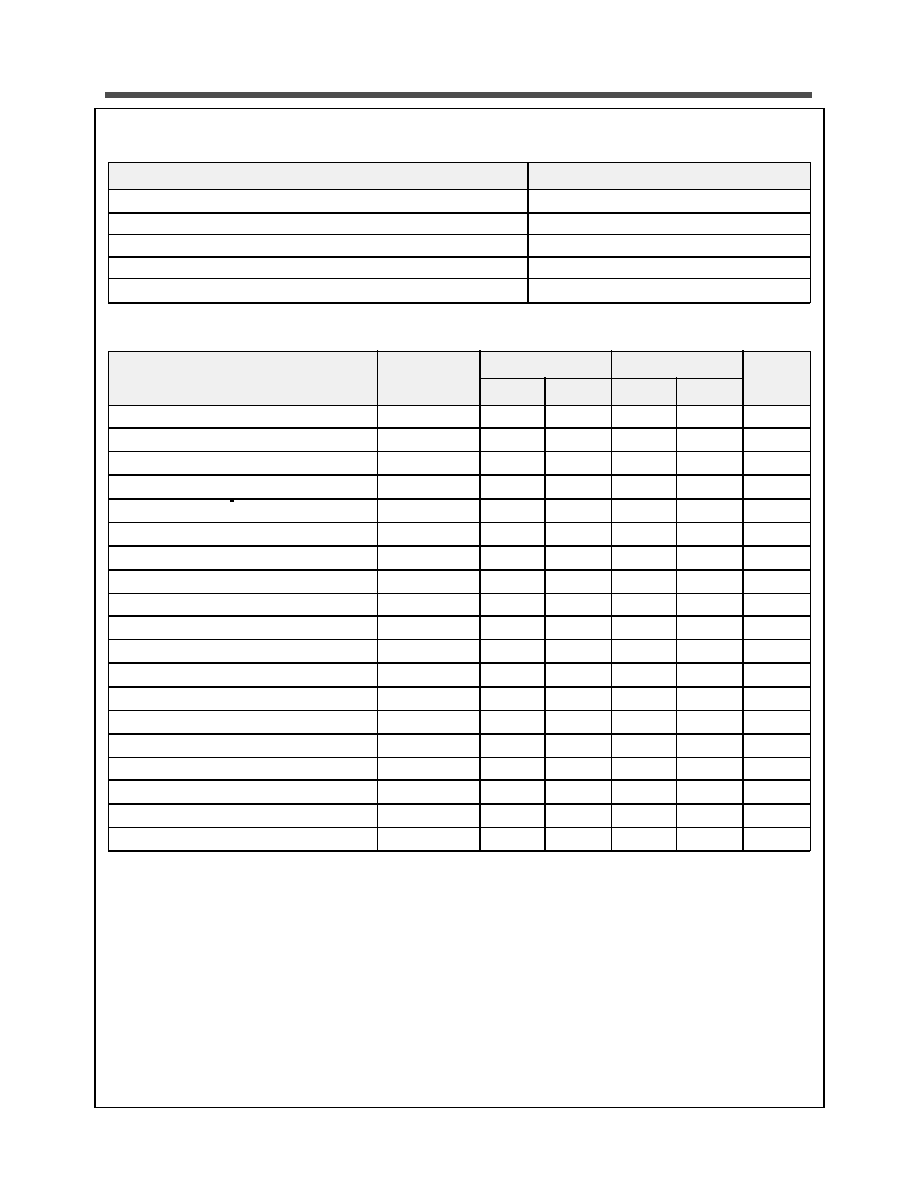
TABLE 5: Timing Test Conditions
TABLE 6: Timing
Item
Input Pulse Level
0.1V
CC
to 0.9 V
CC
Input Rise and Fall Time
5ns
Input and Output Timing Reference Levels
0.5 V
CC
Output Load
CL = 30pF
Operating Temperature
-40 to +85
o
C
Item
Symbol
2.3 - 3.6 V
3.0 - 3.6 V
Units
Min.
Max.
Min.
Max.
Read Cycle Time
t
RC
70
55
ns
Address Access Time
t
AA
70
55
ns
Chip Enable to Valid Output
t
CO
70
55
ns
Output Enable to Valid Output
t
OE
25
20
ns
Chip Enable to Low-Z output
t
LZ
10
10
ns
Output Enable to Low-Z Output
t
OLZ
5
5
ns
Chip Disable to High-Z Output
t
HZ
0
20
0
15
ns
Output Disable to High-Z Output
t
OHZ
0
20
0
15
ns
Output Hold from Address Change
t
OH
10
10
ns
Write Cycle Time
t
WC
70
55
ns
Chip Enable to End of Write
t
CW
50
45
ns
Address Valid to End of Write
t
AW
50
45
ns
Write Pulse Width
t
WP
40
35
ns
Address Setup Time
t
AS
0
0
ns
Write Recovery Time
t
WR
0
0
ns
Write to High-Z Output
t
WHZ
20
15
ns
Data to Write Time Overlap
t
DW
40
35
ns
Data Hold from Write Time
t
DH
0
0
ns
End Write to Low-Z Output
t
OW
5
5
ns

Stock No. 23033-A
Advance Information - Subject to Change Without Notice
5
EM128L08
NanoAmp Solutions, Inc.
Advance Information
FIGURE 3: Read Cycle Timing (WE = V
IH
)
FIGURE 4: Write Cycle Timing (OE clock)
A0-A16
CE1/CE2
OE
D0-D7
t
RC
t
CE
t
OE
t
OHZ
t
HZ
t
AA
Data Valid
t
LZ
t
OH
t
OLZ
Enable Valid
A0-A16
OE
CE1/CE2
WE
Data In
Data Out
t
WC
t
AW
t
CW
t
WP
t
WHZ
t
DW
t
DH
Data
High-Z
t
WR
t
OHZ
t
OW
t
AS
Enable Valid