This Data Sheet may be revised by subsequent versions ©2003 Eon Silicon Solution, Inc., www.essi.com.tw
or modifications due to changes in technical specifications.
1
EN29F002A / EN29F002AN
Rev. A, Issue Date: 2003/03/26
FEATURES
· 5.0V ± 10% for both read/write operation
· Read Access Time
- 45ns, 55ns, 70ns, and 90ns
· Fast Read Access Time
- 70ns with C
load
= 100pF
- 45ns, 55ns with C
load
= 30pF
· Sector Architecture:
One 16K byte Boot Sector, Two 8K byte
Parameter Sectors, one 32K byte and
three 64K byte main Sectors
· Boot Block Top/Bottom Programming
Architecture
· High performance program/erase speed
- Byte program time: 10µs typical
- Sector erase time: 500ms typical
- Chip erase time: 3.5s typical
· Low Standby Current
- 1µA CMOS standby current-typical
- 1mA TTL standby current
· Low Power Active Current
- 30mA active read current
- 30mA program / erase current
· JEDEC Standard program and erase
commands
· JEDEC standard DATA polling and toggle
bits feature
· Hardware
RESET
Pin
(n/a on EN29F002AN)
· Single Sector and Chip Erase
· Sector Protection / Temporary Sector
Unprotect (RESET = V
ID
)
· Sector Unprotect Mode
· Embedded Erase and Program Algorithms
· Erase Suspend / Resume modes:
Read and program another sector during
Erase Suspend Mode
· 0.23 µm triple-metal double-poly
triple-well CMOS Flash Technology
· Low Vcc write inhibit < 3.2V
· 100K endurance cycle
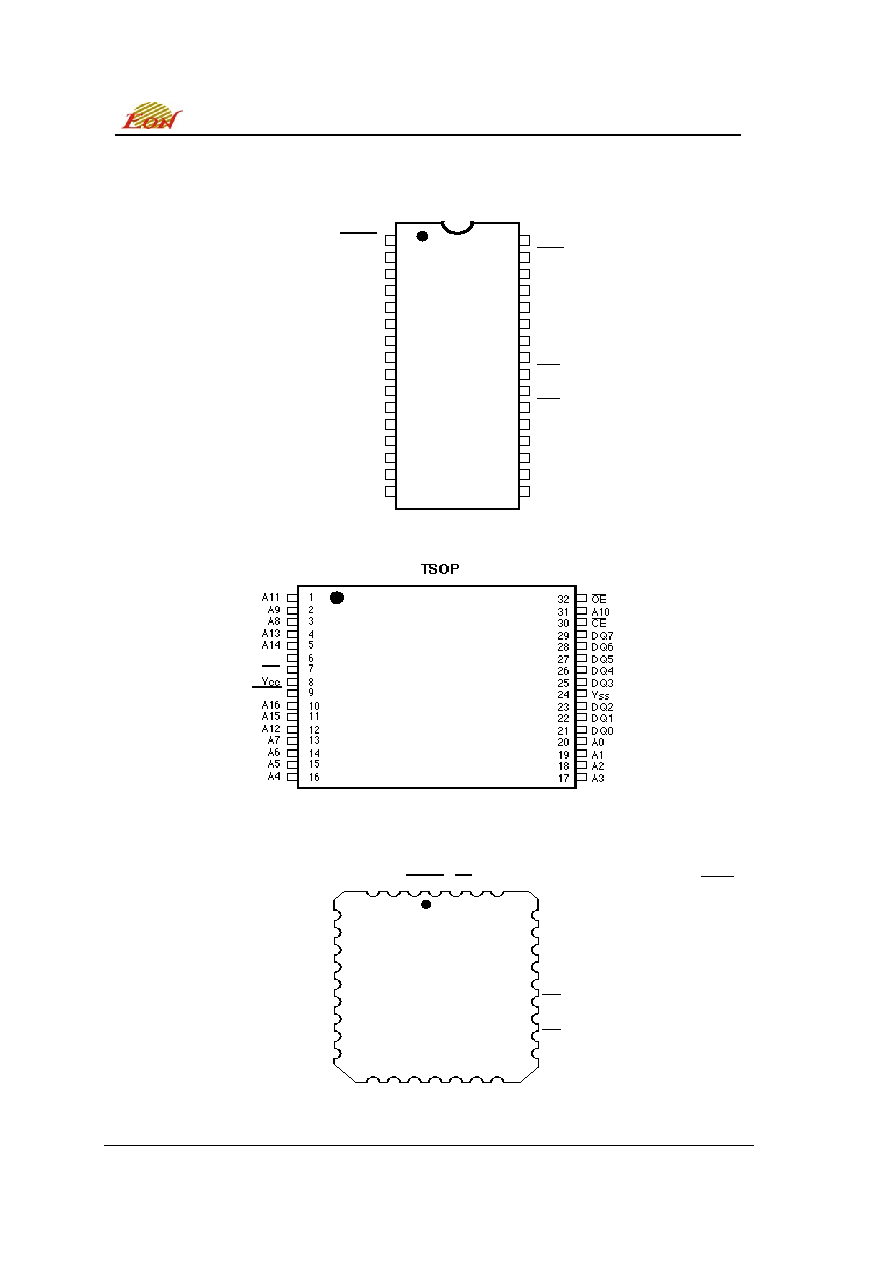
· Package Options
- 32-pin PDIP
- 32-pin PLCC
- 32-pin TSOP (Type 1)
· Commercial and Industrial Temperature
Ranges
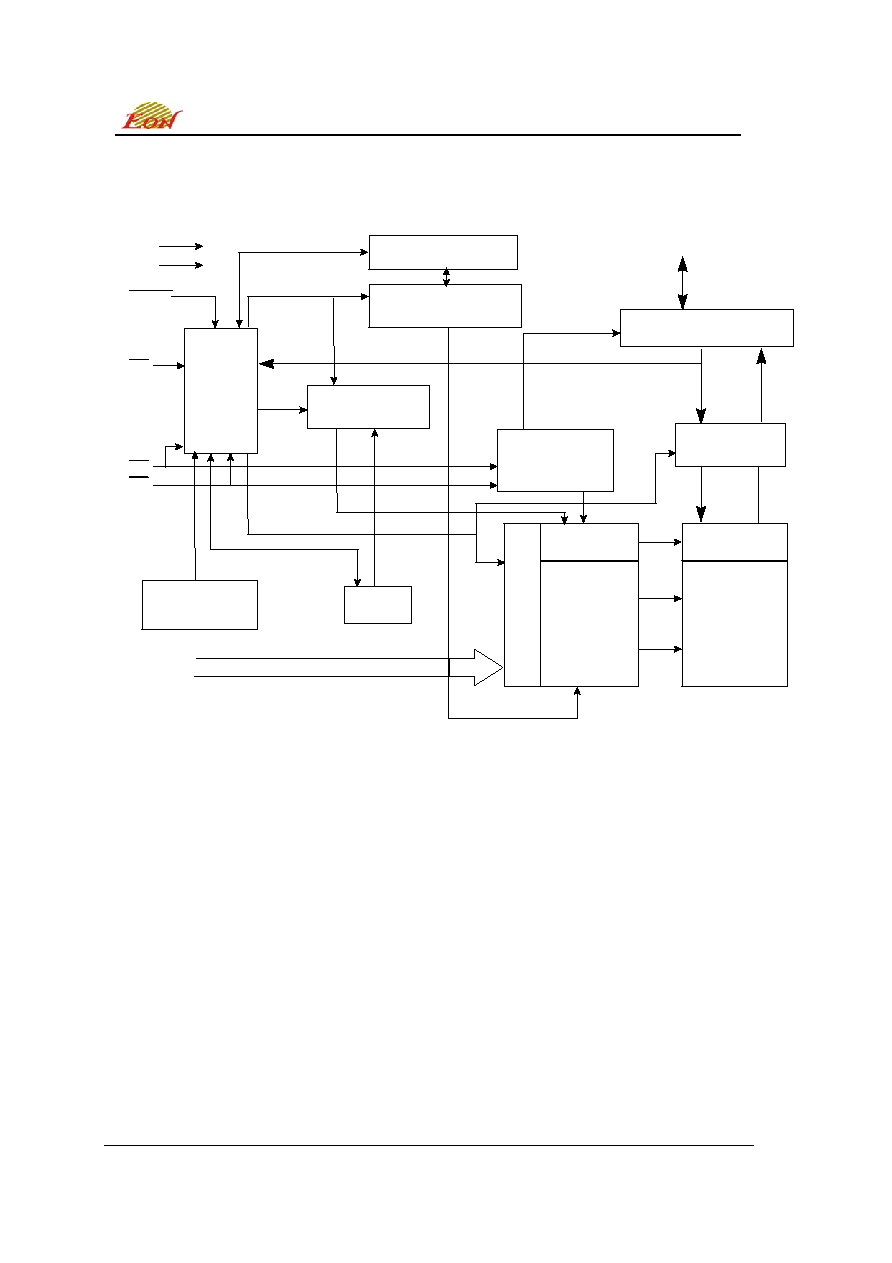
GENERAL DESCRIPTION
The EN29F002A / EN29F002AN is a 2-Megabit, electrically erasable, read/write non-volatile flash memory.
Organized into 256K words with 8 bits per word, the 2M of memory is arranged in seven sectors (with
top/bottom configuration), including one 16K Byte Boot Sector, two 8K Byte Parameter sectors, and four main
sectors (one 32K Byte and three 64K Byte). Any byte can be programmed typically at 10µs. The EN29F002A /
EN29F002AN features 5.0V voltage read and write operation. The access times are as fast as 45ns to
eliminate the need for WAIT states in high-performance microprocessor systems.
The EN29F002A / EN29F002AN has separate Output Enable ( OE ), Chip Enable (
CE
), and Write
Enable (
W E
) controls which eliminate bus contention issues. This device is designed to allow
either single sector or full chip erase operation, where each sector can be individually protected
against program/erase operations or temporarily unprotected to erase or program. The device can
sustain a minimum of 100K program/erase cycles on each sector.
EN29F002A / EN29F002AN
2 Megabit (256K x 8-bit) Flash Memory
This Data Sheet may be revised by subsequent versions ©2003 Eon Silicon Solution, Inc., www.essi.com.tw
or modifications due to changes in technical specifications.
2
EN29F002A / EN29F002AN
Rev. A, Issue Date: 2003/03/26
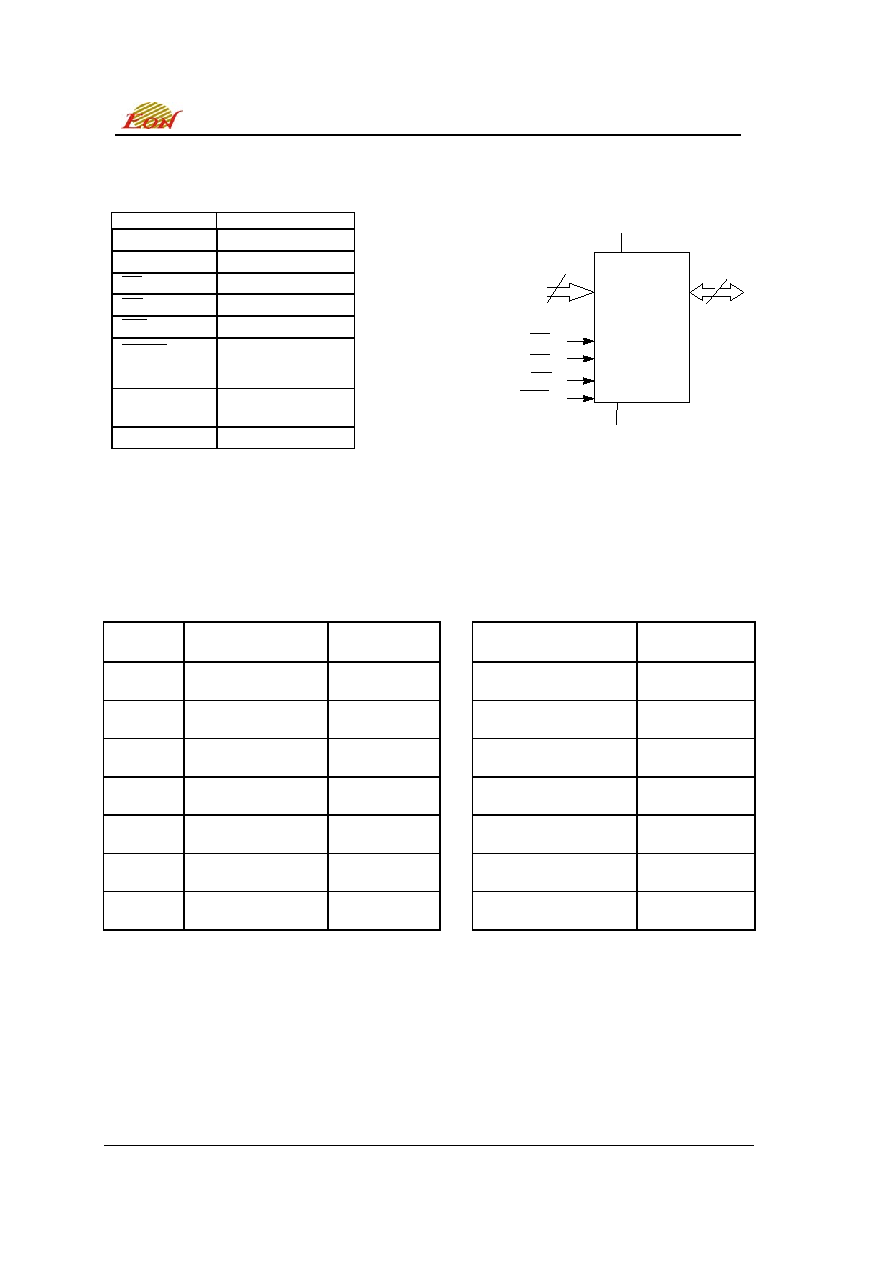
TABLE 1. PIN DESCRIPTION
FIGURE 1. LOGIC DIAGRAM
Pin Name
Function
A0-A17 Addresses
DQ0-DQ7 Data
Input/Outputs
CE
Chip Enable
OE
Output Enable
W E
Write Enable
RESET
(n/a for
EN29F002AN)
Hardware Reset
Sector Unprotect
Vcc Supply
Voltage
(5V
± 10% )
Vss Ground
TABLE 2. BLOCK ARCHITECTURE
TOP BOOT BLOCK
BOTTOM BOOT BLOCK
SECTOR
ADDRESSES
SIZE (Kbytes)
ADDRESSES
SIZE (Kbytes)
6
3C000h - 3FFFFh
16
30000h - 3FFFFh
64
5
3A000h - 3BFFFh
8
20000h - 2FFFFh
64
4
38000h - 39FFFh
8
10000h - 1FFFFh
64
3
30000h - 37FFFh
32
08000h - 0FFFFh
32
2
20000h - 2FFFFh
64
06000h - 07FFFh
8
1
10000h - 1FFFFh
64
04000h - 05FFFh
8
0
00000h - 0FFFFh
64
00000h - 03FFFh
16
EN29F002AT/B
8
DQ0 - DQ7
A0 - A17
18
Vcc
WE
CE
OE
RESET
Vss
N/A on EN29F002AN
This Data Sheet may be revised by subsequent versions ©2003 Eon Silicon Solution, Inc., www.essi.com.tw
or modifications due to changes in technical specifications.
5
EN29F002A / EN29F002AN
Rev. A, Issue Date: 2003/03/26
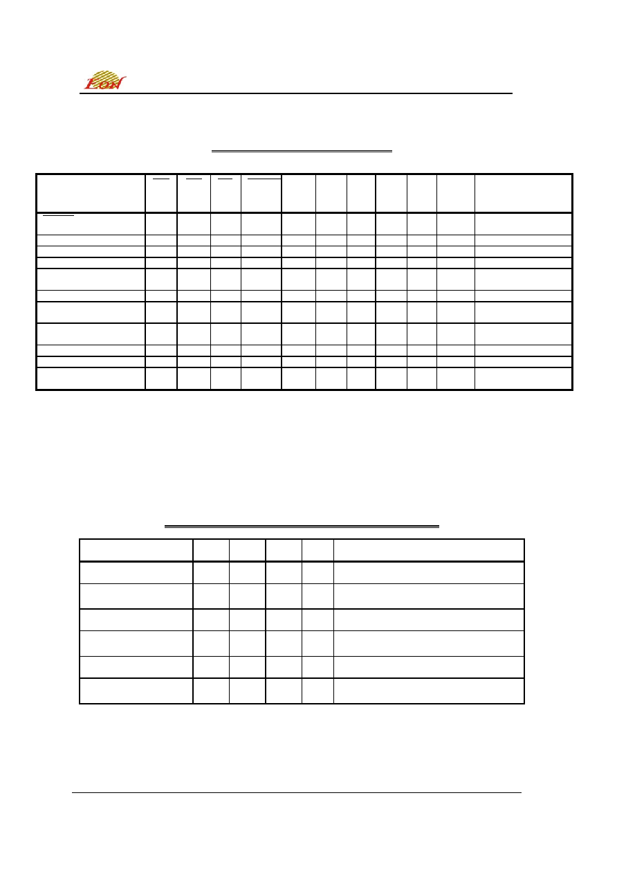
TABLE 3. OPERATING MODES
2M FLASH USER MODE TABLE
USER MODE
C E
WE
OE
R ESE T
A9 A8
A6
A1
A0
Ax/y
DQ(0-7)
RESET
(n/a on EN29F002AN)
X X X L X X X X X X
HI-Z
STANDBY H
X
X
H
X
X
X
X
X
X
HI-Z
READ L
H
L
H
A9
A8
A6
A1
A0
Ax/y
DQ(0-7)
OUTPUT
DISABLE
L H H H X X X X X X
HI-Z
READ
MANUFACTURER ID
L H L H VID
L/H
L L L X MANUFACTURER
ID
READ DEVICE ID
L
H
L
H
VID
L/H
L
L
H
X
DEVICE ID(T/B)
VERIFY SECTOR
PROTECT
L H L H VID X L H L X
01h(protected)
00h(unprotected)
ENABLE SECTOR
PROTECT
L L
VID H VID
X L X X X
X
SECTOR
UNPROTECT L L VID H VID X H H L X
X
WRITE L
L
H
H
A9
A8
A6
A1
A0
Ax/y
DIN(0-7)
TEMPORARY SECTOR
UNPROTECT
X X X VID X X X X X X
X
NOTES:
1) L = V
IL
, H = V
IH
, V
ID
= 11.0V
± 0.5V
2) X = Don't care, either V
IH
or V
IL
TABLE 4. DEVICE IDENTIFICTION
2M FLASH MANUFACTURER/DEVICE ID TABLE
A8
A6
A1
A0
DQ(7-0)
HEX
READ
MANUFACTURER ID
L L L L CONTINUATION
MANUFACTURER
ID
7F
READ
MANUFACTURER ID
*
H
L
L
L
MANUFACTURER ID
1C
READ DEVICE ID
(Top Architecture)
L
L
L
H
CONTINUATION DEVICE ID
7F
READ DEVICE ID
*
(Top Architecture)
H L L H
DEVICE
ID
92
READ DEVICE ID
(Bottom Architecture)
L
L
L
H
CONTINUATION DEVICE ID
7F
READ DEVICE ID
*
(Bottom Architecture)
H L L H
DEVICE
ID
97
NOTES:
These modes (A8=H) are recommended for Manufacture/Device ID check.