
ESS Technology, Inc.
SAM0523B-031804
1
ESS Technology, Inc.
ES6168A
Vibratto-S DVD Processor
Product Brief
DESCRIPTION
The ES6168A Vibratto
S DVD processor is a super high-
performance single-chip MPEG video decoding solution
that provides not only DVD decoding, but also MPEG-4
support, allowing users to view video clips (from the
Internet, a camcorder, or other source) on DVD players.
The ES6168A integrates a state-of-the-art progressive-
scan video feature to provide brilliant and sharp, flicker-
free output to the video display, built-in CPRM, and S/PDIF
input and output support. The ES6168A performs
audio/video stream data processing, TV encoding,
Macrovision
copy protection, DVD system navigation,
system control, and housekeeping functions.
The Vibratto-S DVD processor is built on the ESS
p rop rie tar y d u al CPU P ro g ra m m ab l e M u l ti m e d i a
Processor (PMP) core consisting of 32-bit RISC and 64-bit
DSP processors and offers the best DVD feature set. The
processing units enable simultaneous parallel execution of
system commands and data processing to perform
specialized encoding and decoding tasks.
The RISC processor performs bit stream parsing, control
audio data output, transfer video and audio data to the
v e c t o r e n g i n e a n d s e r v i c e s y s t e m c o n t r o l a n d
housekeeping functions. The vector engine performs
audio and video micro-code processing required by A/V
standards, such as Dolby
Digital, MPEG and JPEG
imaging. These processing tasks include video motion
compensation and estimation, loop filtering, Discrete
Cosine Transforms (DCT), inverse DCT, quantization, and
inverse quantization.
The Vibratto-S DVD processor supports both parallel and
serial DVD loader interfaces, industry standard I
2
S audio
data input and output, EPROM and DRAM access, and
audio/video data buffering. It also supports both letterbox
and pan-and-scan displays, sub-picture overlay, and On-
Screen Display (OSD). In addition, the Vibratto-S DVD
solution plays Karaoke, CD+G, DVD-Audio, HDCD, CD-
DA, MP3, and WMA.
The ES6168A DVD processor is available in a 208-pin
Plastic Quad Flat Pack (PQFP) device package.
FEATURES
�
Single-chip DVD processor.
�
MPEG-4 Advanced Simple Profile* at full screen (D1).
�
Integrated NTSC/PAL encoder with pixel-adaptive
de-interlacer and five 10-bit 54 MHz video DACs.
�
High-quality progressive scan video output for flicker-free
video display.
�
DVD-Video, DVD-VR, VCD 1.1 and 2.0, and SVCD.
�
Full DVD-Audio support including MLP and LPCM
decode, CPPM decryption, and watermark detection.
�
Media playback with CD-ROM, CD-R/RW, DVD-R/RW,
DVD+R/RW, and DVD-RAM.
�
Up to 7.1 channel audio outputs.
�
Interface for IDE devices, A/V DVD loaders.
�
Interface for CF, MS, SD, MMC, and SM memory cards.
�
Direct interface of 8-/16-bit DRAM up to 128-Mb capacity.
�
Direct interface for up to 4 banks of 8-/16-bit EPROM or
Flash EPROM for up to 4-MB for each bank.
�
Macrovision 7.1 for NTSC/PAL interlaced video.
�
Macrovision NTSC/PAL (480p/576p) progressive scan
video.
�
Simultaneous composite, S-video, and YUV outputs.
�
CCIR 656/601 YUV 4:2:2 input and output.
�
On-Screen Display controller supports 256 colors in 8
degrees of transparency.
�
Subpicture Unit (SPU) decoder supports karaoke lyric,
subtitles, and EIA-608 compliant Line 21 Captioning.
�
SmartLogo
for custom JPEG wallpaper.
�
JPEG digital photo support (Kodak Picture CD
and
Fujifilm FujiColor CD
).
�
ESS Music SlideshowTM.
�
Bass management.
�
Dolby Digital (AC-3), Dolby Pro LogicTM, and Pro Logic II.
�
DTS
surround.
�
S/PDIF digital audio input and output.
�
MPEG AAC and Multichannel.
�
SRS TruSurround
and
TruSurround
XT
.
�
WindowsTM Media Audio decoding.
�
Professional karaoke with full scoring scheme.
ESS Technology, Inc.
SAM0523B-031804
3
ES6168A PRODUCT BRIEF
ES6168A PIN DESCRIPTION
ES6168A PIN DESCRIPTION
Table 1 lists the pin descriptions for the ES6168A.
Table 1 ES6168A Pin Description
Name
Pin Numbers
I/O
Definition
VEE
1,18, 27, 59, 68, 75,
92, 99, 104, 130,
148, 157, 159, 164,
183, 193, 201
P
I/O power supply.
LA[21:0]
2-7, 10-16, 19-23,
204-207
O
RISC port address bus.
VSS
8, 17, 26, 34, 43,
60, 67, 76, 84, 91,
98, 103, 120, 129,
138, 147, 156, 163,
171, 177, 184, 192,
200, 208
G
Ground.
VCC
9, 35, 44, 83, 121,
139, 172
P
Core power supply.
RESET#
24
I
Reset input; (5V tolerant input).
TDMDX
25
O
TDM transmit data output.
RSEL
I
LCS3 ROM Boot Data Width Select. Strapped to VCC or ground via 4.7-k
resistor; read only during reset.
TDMDR
28
I
TDM receive data input; (5V tolerant input).
TDMCLK
29
I
TDM clock input; (5V tolerant input).
TDMFS
30
I
TDM frame sync input; (5V tolerant input).
TDMTSC#
31
O
TDM output enable.
TWS
32
O
Audio transmit frame sync output.
SEL_PLL2
I
System and DSCK output clock frequency selection is made at the rising edge of
RESET#. The matrix below lists the available clock frequencies and their
respective PLL bit settings. Strapped to VCC or ground via 4.7-k
resistor; read
only during reset.
RSEL
Selection
0
16-bit ROM
1
8-bit ROM
SEL_PLL2
SEL_PLL1
SEL_PLL0
PLL Settings
0
0
0
DCLK
� 4
.5
0
0
1
DCLK
�
5.0
0
1
0
Bypass
0
1
1
DCLK
�
4.0
1
0
0
DCLK
�
4.25
1
0
1
DCLK
�
4.75
1
1
0
DCLK
�
5.5
1
1
1
DCLK
�
6.0
4
SAM0523B-031804
ESS Technology, Inc.
ES6168A PRODUCT BRIEF
ES6168A PIN DESCRIPTION
TSD0
33
O
Audio transmit serial data output 0.
SEL_PLL0
I
Refer to the description and matrix for SEL_PLL2 pin 32.
TSD1
36
O
Audio transmit serial data output 1.
SEL_PLL1
I
Refer to the description and matrix for SEL_PLL2 pin 32.
TSD2
37
O
Audio transmit serial data output 2. This pin must be pulled down to VSS via a
4.7-k
resistor for proper operation.
TSD3
38
O
Audio transmit serial data output 3.
MCLK
39
I/O
Audio master clock for audio DAC.
TBCK
40
I/O
Audio transmit bit clock. TBCK is an input during reset and subsequently is
programmed as an output via the AUDIOXMT register (addr 0x2000D00Ch, bit 4).
SEL_PLL3
41
I
Clock source select. Strapped to VCC or ground via 4.7-k
resistor; read only
during reset.
SPDIF_OUT
O
S/PDIF output.
SPDIF_IN
42
I
S/PDIF input; (5V tolerant input).
RSD
45
I
Audio receive serial data; (5V tolerant input).
RWS
46
I
Audio receive frame sync; (5V tolerant input).
RBCK
47
I
Audio receive bit clock; (5V tolerant input).
CAMIN3
48
I
Camera YUV 3.
PIXIN3
I
CCIR656 input pixel 3.
XIN
49
I
27-MHz crystal input.
XOUT
50
O
27-MHz crystal output.
AVEE
51
P
Analog power for PLL.
AVSS
52
G
Analog ground for PLL.
DMA[11:0]
53-58, 61-66
O
DRAM address bus.
DCAS#
69
O
DRAM column address strobe.
DOE#
70
O
DRAM output enable.
DSCK_EN
O
DRAM clock enable.
DWE#
71
O
DRAM write enable.
DRAS#
72
O
DRAM row address strobe.
DMBS0
73
O
DRAM bank select 0.
DMBS1
74
O
DRAM bank select 1.
DB[15:0]
77-82, 85-90, 93-96
I/O
DRAM data bus.
DCS[1:0]#
97,100
O
DRAM chip select.
DQM
101
O
Data input/output mask.
DSCK
102
O
Output clock to DRAM.
Table 1 ES6168A Pin Description (Continued)
Name
Pin Numbers
I/O
Definition
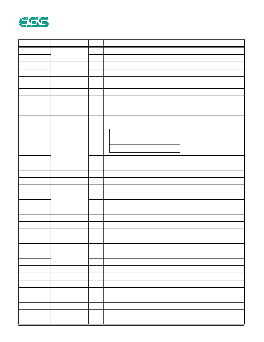
SEL_PLL3
Clock Source
0
Crystal oscillator
1
DCLK input

