 | –≠–ª–µ–∫—Ç—Ä–æ–Ω–Ω—ã–π –∫–æ–º–ø–æ–Ω–µ–Ω—Ç: ESC1621 | –°–∫–∞—á–∞—Ç—å:  PDF PDF  ZIP ZIP |

p. 1
Last update: 2004-03-05 12:03
***********************************************************************************************************
General Descriptions
The ESC1621 is a 128-pattern (32x4), memory mapping, and multi-function LCD driver. The
S/W configuration feature of the ESC1621 makes it suitable for multiple LCD applications includ-
ing LCD modules and display subsystems. Only three or four lines are required for the interface
between the host controller and the ESC1621. The ESC1621 contains a power down command to
reduce power consumption.
Features
∑
Operating voltage: 2.4V~5.2V.
∑
Built-in 256kHz RC oscillator.
∑
External 32.768kHz crystal or 256kHz frequency source input.
∑
Selection of 1/2 or 1/3 bias, and selection of 1/2 or 1/3 or 1/4 duty LCD applications.
∑
Internal time base frequency sources.
∑
Two selectable buzzer frequencies (2kHz/4kHz).
∑
Built-in time base generator and WDT.
∑
Time base or WDT overflow output.
∑
Power down command reduces power Consumption.
∑
8 kinds of time base/WDT clock sources.
∑
32x4 LCD driver.
∑
Built-in 32x4 bit display RAM.
∑
3-wire serial interface.
∑
Internal LCD driving frequency source.
∑
Software configuration feature.
∑
Data mode and command mode instructions.
∑
R/W address auto increment.
∑
Three data accessing modes.
∑
VLCD pin for adjusting LCD operating voltage.
RAM Mapping 32 X 4 LCD Controller for I/O uC

ESC1621
p. 2
Last update: 2004-03-05 12:13
Block Diagram
Note:
CS: Chip selection
BZ,
BZ: Tone outputs
WR,
RD, DATA: Serial interface
IRQ: Time base or WDT overflow output
COM0~COM3, SEG0~SEG31: LCD outputs
Tone
Generator
Watchdog Timer
&
Time Base Generator
Control
Logic
&
Timing
Generator
LCD Driver
&
Bias Circuit
Display Memory
OSCO
OSCI
DATA
GND
VDD
VLCD
COM0
COM3
SEG0
SEG31
BZ
BZ
CS
RD
WR
IRQ
ESC1621
p. 3
Last update: 2004-03-05 12:13
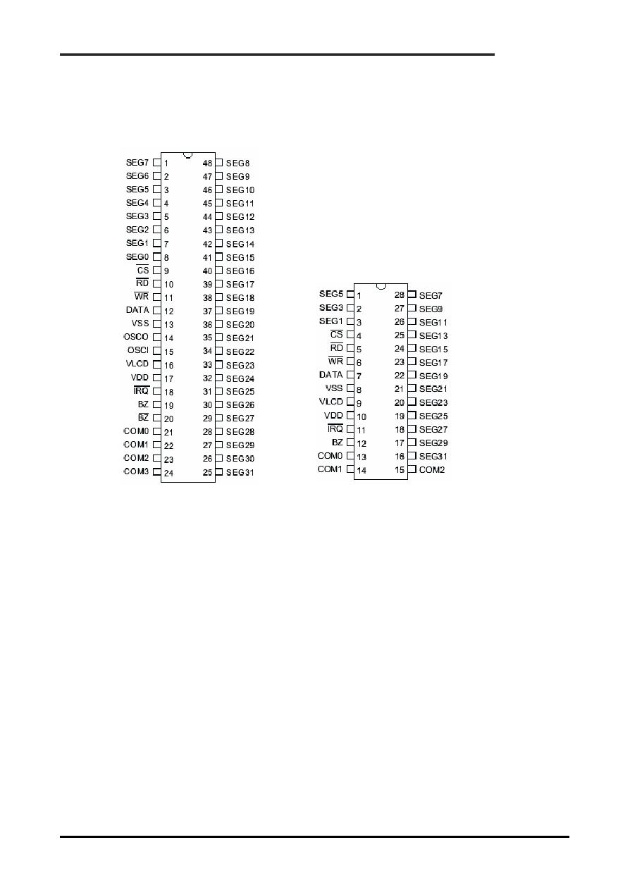
Pin Assignment
ESC1621B-48SSOP
ESC1621D-28SKDIP

ESC1621
p. 4
Last update: 2004-03-05 12:13
Pad Description
Pad No.
Pad Name
I/O
Function
1
CS
I
Chip selection input with pull-high resistor
When the
CS
is logic high, the data and command read from or written
to the ESC1621 are disabled. The serial interface circuit is also reset. But
if
CS
is at logic low level and is input to the
CS
pad, the data and com-
mand transmission between the host controller and the ESC1621 are all
enabled.
2
RD
I
READ clock input with pull-high resistor
Data in the RAM of the ESC1621 are clocked out on the falling edge of
the
RD
signal. The clocked out data will appear on the DATA line. The
host controller can use the next rising edge to latch the clocked out data.
3
WR
I
WRITE clock input with pull-high resistor
Data on the DATA line are latched into the ESC1621 on the rising edge
of the
WR
signal.
4
DATA
I/O Serial data input/output with pull-high resistor
5
GND
-- Negative power supply, ground
6
OSCO
O
7
OSCI
I
The OSCI and OSCO pads are connected to a 32.768kHz crystal in order
to generate a system clock. If the system clock comes from an external
clock source, the external clock source should be connected to the OSCI
pad. But if and on-chip RC oscillator is selected instead, the OSCI and
OSCO pads can be left open.
8
VLCD
I
LCD power input
9
VDD
-- Positive power supply
10
IRQ
O
Time base or WDT overflow flag, NMOS open drain output
11,12
BZ,
BZ
O
2kHz or 4kHz tone frequency output pair
13~16
COM0~COM3
O
LCD common outputs
48~17
SEG0~SEG31
O
LCD segment outputs
Absolute Maximum Ratings
Supply Voltage....................... -0.3V ~ 5.5V
Input Voltage... ... ... V
SS
- 0.3V ~ V
DD
+ 0.3V
Storage Temperature... ... ... ... ... -50
∞
C ~ 125
∞
C
Operating Temperature... ... ... ... . . -25
∞
C ~ 75
∞
C
Note: These are stress ratings only. Stresses exceeding the range specified under "Absolute Maxi-
mum Ratings" may cause substantial damage to the device. Functional operation of this de-
vice at other conditions beyond those listed in the specification is not implied and prolonged
exposure to extreme conditions may affect device reliability.
ESC1621
p. 5
Last update: 2004-03-05 12:13
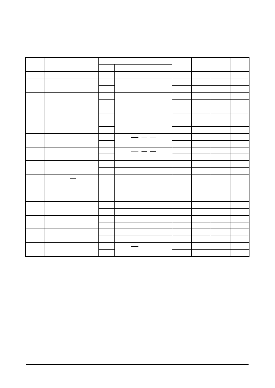
D.C. Characteristics
Test Conditions
Symbol
Parameter
V
DD
Conditions
Min.
Typ.
Max.
Unit
V
DD
Operating Voltage
--
--
2.4
--
5.2
V
3V
--
220
300
µA
I
DD1
Operating Current
5V
No load/LCD ON
On-chip RC oscillator
--
450
600
µA
3V
--
90
120
µA
I
DD2
Operating Current
5V
No load/LCD ON
Crystal oscillator
--
180
240
µA
3V
--
150
200
µA
I
DD3
Operating Current
5V
No load/LCD ON
External clock source
--
300
400
µA
3V
--
0.1
5
µA
I
STB
Standby Current
5V
No load
Power down mode
--
0.3
10
µA
3V
0
--
0.6
V
V
IL
Input Low Voltage
5V
DATA,
WR
,
CS
,
RD
0
--
1.0
V
3V
2.4
--
3.0
V
V
IH
Input High Voltage
5V
DATA,
WR
,
CS
,
RD
4.0
--
5.0
V
3V
V
OL
=0.3V
0.5
1.2
--
mA
I
OL1
DATA, BZ,
BZ
,
IRQ
5V
V
OL
=0.5V
1.3
2.6
--
mA
3V
V
OH
=2.7V
-0.4
-0.8
--
mA
I
OH1
DATA, BZ,
BZ
5V
V
OH
=4.5 V
-0.9
-1.8
--
mA
3V
V
OL
=0.3V
80
150
--
µA
I
OL2
LCD Common Sink Current
5V
V
OL
=0.5V
150
250
--
µA
3V
V
OH
=2.7V
-80
-120
--
µA
I
OH2
LCD Common Source Cur-
rent
5V
V
OH
=4.5 V
-120
-200
--
µA
3V
V
OL
=0.3V
60
120
--
µA
I
OL3
LCD Segment Sink Current
5V
V
OL
=0.5V
120
200
--
µA
3V
V
OH
=2.7V
-40
-70
--
µA
I
OH3
LCD Segment Source Cur-
rent
5V
V
OH
=4.5 V
-70
-100
--
µA
3V
40
80
150
kO
R
PH
Pull-high Resistor
5V
DATA,
WR
,
CS
,
RD
30
60
100
kO
ESC1621
p. 6
Last update: 2004-03-05 12:13
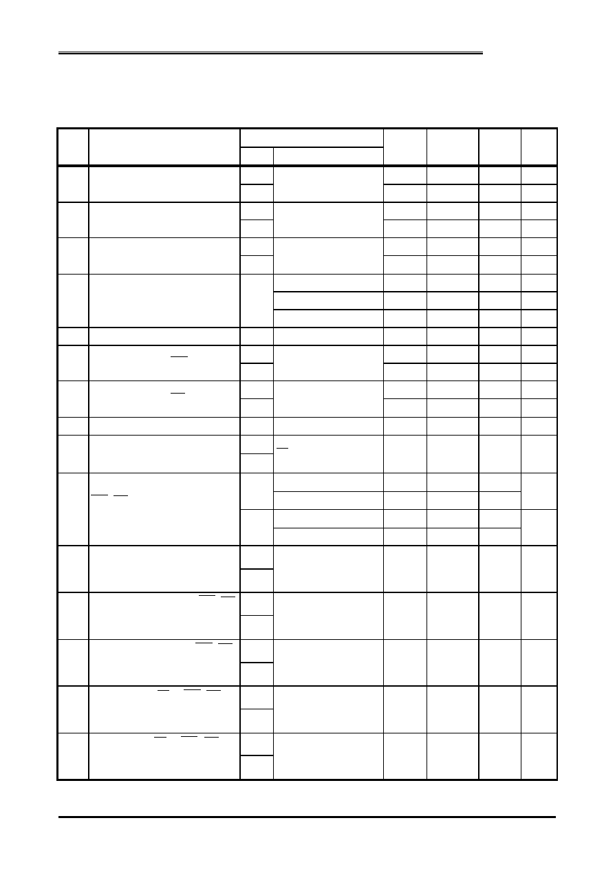
A.C. Characteristics
Test Conditions
Sym.
Parameter
V
DD
Conditions
Min.
Typ.
Max.
Unit
3V
--
256
--
kHz
f
SYS1
System Clock
5V
On-chip RC oscillator
--
256
--
kHz
3V
--
32.768
--
kHz
f
SYS2
System Clock
5V
Crystal oscillator
--
32.768
--
kHz
3V
--
256
--
kHz
f
SYS3
System Clock
5V
External clock source
--
256
--
kHz
On-chip RC oscillator
--
F
SYS1
/1024
--
Hz
Crystal oscillator
--
F
SYS2
/128
--
Hz
f
LCD
LCD Clock
--
External clock source
--
F
SYS3
/1024
--
Hz
t
COM
LCD Common Period
n: Number of COM
--
n/f
LCD
--
s
3V
--
150
kHz
f
CLK1
Serial Data Clock (
WR
Pin)
5V
Duty cycle 50%
--
300
kHz
3V
--
75
kHz
f
CLK2
Serial Data Clock (
RD
Pin)
5V
Duty cycle 50%
--
150
kHz
f
TONE
Tone Frequency
On-chip RC oscillator
--
2.0 or 4.0
--
kHz
3V
t
CS
Serial Interface Reset Pulse Width
(Figure 3) 5V
CS
--
250
--
ns
Write mode
3.34
--
--
3V
Read mode
6.67
--
--
µs
Write mode
1.67
--
--
t
CLK
WR
,
RD
Input Pulse Width
(Figure 1)
5V
Read mode
3.34
--
--
µs
3V
t
r,
t
f
Rise/Fall Time Serial Data Clock
Width
(Figure 1) 5V
--
--
120
--
ns
3V
t
su
Setup Time for DATA to
WR
,
RD
Clock Width
(Figure 2) 5V
--
--
120
--
ns
3V
t
h
Hold Time for DATA to
WR
,
RD
Clock Width
(Figure 2) 5V
--
--
120
--
ns
3V
t
su1
Setup Time for
CS
to
WR
,
RD
Clock Width
(Figure 3) 5V
--
--
100
--
ns
3V
t
h1
Hold Time for
CS
to
WR
,
RD
Clock Width
(Figure 3) 5V
--
--
100
--
ns
ESC1621
p. 7
Last update: 2004-03-05 12:13
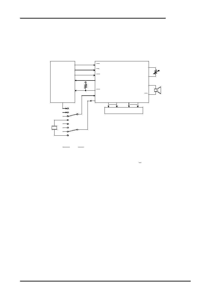
Application Circuits
Host controller with a ESC1621 display system
Note: The connection of
IRQ
and
RD
pin can be selected depending on the requirement of the µC.
The voltage applied to V
LCD
pin must be lower than V
DD.
Adjust VR to fit LCD display, at V
DD
=5V, V
LCD
=4V, VR=15kO+20%
Adjust R (external pull-high resistance) to fit user's time base clock.
DATA
OSCI
OSCO
COM0 COM3
~
SEG0 SEG31
~
VLCD
VDD
BZ
1/2 or 1/3 Bias; 1/2, 1/3 or 1/4 Duty
LCD PANEL
µC
ESC1621
Clock Out
External Clock 1
External Clock 2
On-chip OSC
Crystal
32768Hz
R
*
*
VR
*
Piezo
BZ
IRQ
WR
RD
CS