 | –≠–ª–µ–∫—Ç—Ä–æ–Ω–Ω—ã–π –∫–æ–º–ø–æ–Ω–µ–Ω—Ç: F0522501Q | –°–∫–∞—á–∞—Ç—å:  PDF PDF  ZIP ZIP |
Features
∑ Up to 2.7 Gb/s (FEC available)
high speed operation
∑ Clocked (MS-D/FF) or Non-clocked
operation can be selected
∑ Disable function of modulation current
and bias current
∑ Bias current monitoring
∑ Mark density monitoring
∑ +5 V or -5 V single power supply
∑ Up to 60 mA p-p modulation current
∑ Up to 50 mA bias current
∑ Differential ECL compatible interface
∑ On-chip 50
terminations
∑ Internal voltage reference for AC coupling
Applications
∑ Laser diode driver of an optical transmitter circuit up to 2.7 Gb/s (FEC available)
Functional Description
The F0522501Q is a high performance GaAs laser diode driver IC applicable in an opti-
cal transmitter circuit up to 2.7 Gb/s NRZ data rate (especially suitable for SDH [STM-16] /
SONET [OC-48]) , featuring the capable operation for the FEC signal.
The F0522501Q specifies the rise time and the fall time of 70 ps (20 %-80 %) typically. It
features the single +5 V or -5 V supply operation, the modulation current between 1 mA and
60 mA, and the bias current between 1 mA and 50 mA while the dissipating power is around
the typical value of 1 W.
01.08.28
Laser Diode Driver
2.7 Gb/s NRZ Data Rate
F0522501Q

F0522501Q
2.7 Gb/s Laser Diode Driver
Absolute Maximum Ratings
T
a
=25
∞
C, unless specified
Recommended Operating Conditions
r
e
t
e
m
a
r
a
P
l
o
b
m
y
S
e
u
l
a
V
s
t
i
n
U
e
g
a
t
l
o
V
y
l
p
p
u
S
V
D
D
V
-
S
S
0
.
7
+
o
t
5
.
0
-
V
t
n
e
r
r
u
C
y
l
p
p
u
S
n
o
c
I
0
5
2
A
m
D
(
e
g
a
t
l
o
V
t
u
p
n
I
N
I
D
,
B
N
I
K
C
,
N
I
K
C
,
B
N
I
)
V
N
I
V
S
S
V
o
t
D
D
5
.
0
+
V
S
I
D
(
e
g
a
t
l
o
V
t
u
p
n
I
N
I
L
E
S
,
N
I
)
V
1
C
N
I
V
S
S
V
o
t
D
D
5
.
0
+
V
V
(
e
g
a
t
l
o
V
t
u
p
n
I
N
I
M
V
,
N
I
B
)
V
2
C
N
I
V
S
S
V
o
t
S
S
5
.
1
+
V
T
U
O
,
T
U
O
(
e
g
a
t
l
o
V
t
u
p
t
u
O
B
T
U
O
,
S
A
I
B
)
V
T
U
O
V
D
D
V
o
t
0
.
2
-
D
D
5
.
0
+
V
K
R
M
,
K
R
M
(
e
g
a
t
l
o
V
t
u
p
t
u
O
B
M
B
,
M
B
,
B
)
V
M
T
U
O
V
S
S
V
o
t
D
D
5
.
0
+
V
V
(
e
g
a
t
l
o
V
n
o
i
t
a
n
i
m
r
e
T
D
T
T
V
,
K
C
T
T
)
V
T
T
V
D
D
V
o
t
5
.
2
-
D
D
5
.
0
+
V
e
r
u
t
a
r
e
p
m
e
T
e
g
a
r
o
t
S
g
t
s
T
5
2
1
+
o
t
5
5
-
∞
C
e
r
u
t
a
r
e
p
m
e
T
g
n
i
t
a
r
e
p
O
t
n
e
i
b
m
A
T
a
0
7
+
o
t
0
∞
C
Supply Voltage
Output Voltage
Ambient Operating Temperature
V
DD
-V
SS
V
OUT
T
a
Min.
4.75
V
DD
-1.6
0
Typ.
5.00
V
DD
-1.0
25
Max.
5.46
V
DD
70
V
V
∞
C
Value
Parameter
Symbol
Units

2.7 Gb/s Laser Diode Driver
F0522501Q
Electrical Characteristics
T
a
=25
∞
C, V
DD
- V
SS
=4.75 to 5.46 V
(1) Excluding the input current, the modulation current and the bias current.
(2) Modulation peak current is measured at "OUT" pin.
(3) Rise time and fall time are measured at "OUT" pin.
r
e
t
e
m
a
r
a
P
l
o
b
m
y
S
s
n
o
i
t
i
d
n
o
C
t
s
e
T
e
u
l
a
V
s
t
i
n
U
.
n
i
M
.
p
y
T
.
x
a
M
t
n
e
r
r
u
C
t
i
u
c
r
i
C
)
1
(
I
T
K
C
V
N
I
M
V
=
N
I
B
V
=
S
S
-
0
0
1
0
3
1
A
m
)
L
C
E
(
e
g
a
t
l
o
V
t
u
p
n
I
V
H
I
t
u
p
n
I
l
a
i
t
n
e
r
e
f
f
i
D
V
D
D
0
.
1
-
V
D
D
9
.
0
-
V
D
D
7
.
0
-
V
V
L
I
V
D
D
9
.
1
-
V
D
D
7
.
1
-
V
D
D
6
.
1
-
V
)
C
A
(
e
g
a
t
l
o
V
t
u
p
n
I
V
N
I
t
u
p
n
I
l
a
i
t
n
e
r
e
f
f
i
D
6
.
0
8
.
0
2
.
1
V
p
-
p
r
o
t
s
i
s
e
R
t
u
p
n
I
R
N
I
-
-
0
5
-
k
a
e
P
n
o
i
t
a
l
u
d
o
M
t
n
e
r
r
u
C
)
2
(
I
X
A
M
M
V
N
I
M
V
=
S
S
V
5
.
1
+
0
6
-
-
A
m
I
N
I
M
M
V
N
I
M
V
=
S
S
-
-
0
.
1
A
m
I
S
I
D
M
V
N
I
S
I
D
V
=
D
D
V
5
.
1
-
-
-
5
.
0
A
m
t
n
e
r
r
u
C
s
a
i
B
I
X
A
M
B
V
N
I
B
V
=
S
S
V
5
.
1
+
0
5
-
-
A
m
I
N
I
M
B
V
N
I
B
V
=
S
S
-
-
0
.
1
A
m
I
S
I
D
B
V
N
I
S
I
D
V
=
D
D
V
5
.
1
-
-
-
5
.
0
A
m
)
L
E
S
(
e
g
a
t
l
o
V
t
u
p
n
I
V
H
I
L
E
S
.
p
o
d
e
k
c
o
l
C
-
n
o
N
V
D
D
5
.
1
-
-
V
D
D
V
V
L
I
L
E
S
n
o
i
t
a
l
e
p
o
d
e
k
c
o
l
C
V
S
S
N
E
P
O
V
S
S
5
.
1
+
V
)
S
I
D
(
e
g
a
t
l
o
V
t
u
p
n
I
V
H
I
S
I
D
n
o
i
t
a
l
e
p
o
e
l
b
a
s
i
D
V
D
D
5
.
1
-
-
V
D
D
V
V
L
I
S
I
D
n
o
i
t
a
l
e
p
o
e
l
b
a
n
E
V
S
S
N
E
P
O
V
S
S
5
.
1
+
V
r
o
t
s
i
s
e
R
r
o
t
i
n
o
M
s
a
i
B
R
M
B
-
0
1
-
r
o
t
i
n
o
M
y
t
i
s
n
e
D
k
r
a
M
e
g
a
t
l
o
V
V
(
K
R
M
-
V
B
K
R
M
)
e
d
o
M
l
a
i
t
n
e
r
e
f
f
i
D
"
H
"
ll
A
:
e
t
a
D
-
2
.
1
-
V
e
m
i
T
e
s
i
R
)
3
(
r
t
5
1
=
L
R
%
0
8
-
%
0
2
-
0
7
0
5
1
s
p
e
m
i
T
ll
a
F
)
3
(
f
t
5
1
=
L
R
%
0
2
-
%
0
8
-
0
7
0
5
1
s
p
e
m
i
T
p
u
t
e
S
s
t
-
0
0
1
-
s
p
e
m
i
T
d
l
o
H
h
t
-
0
5
-
s
p
k
c
o
l
C
m
u
m
i
x
a
M
y
c
n
e
u
q
e
r
F
x
a
m
f
V
L
E
S
r
o
N
E
P
O
=
V
S
S
V
o
t
S
S
V
5
.
1
+
7
.
2
-
-
z
H
G
e
t
a
R
a
t
a
D
m
u
m
i
x
a
M
r
p
o
f
V
L
E
S
V
=
D
D
V
o
t
V
5
.
1
-
D
D
7
.
2
-
-
s
p
b
G
F0522501Q
2.7 Gb/s Laser Diode Driver
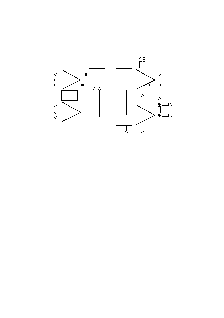
Block Diagram
Pin Descriptions
D
IN
: Positive data input
D
INB
: Negative data input
V
TTD
: Termination for data input
CK
IN
: Positive clock input
CK
INB
: Negative clock input
V
TTCK
: Termination for clock input
OUT
: Positive modulation output (LD should be connected to this pin.)
OUT
B
: Negative modulation output (R
OUTB
=15
typ.)
OUT
BIAS
: Bias output (R
BM
=10
typ., R
BMO
=R
BMOB
=3 k
typ.)
V
MIN
: Voltage input that sets the LD modulation peak current
V
BIN
: Voltage input that sets the LD bias current
DIS
IN
: Voltage input that controls turning on/off the modulation current and the bias
current
SEL
IN
: Voltage input that selects clocked or non-clocked operation
BM
: Bias current monitor positive output
BM
B
: Bias current monitor negative output
MRK
: Mark density monitor positive output (R
MRK
=25 k
typ.)
MRK
B
: Mark density monitor negative output (R
MRKB
=25 k
typ.)
+
Mod.
Circuit
≠
Bias
circuit
+
Input
Buffer
≠
Vref
Generator
+
Input
Buffer
≠
Control
Circuit
Selector
D/FF
DIN
VTTD
DINB
CKIN
VTTCK
CKINB
SELIN DISIN
VBIN
VMIN
RMRK
RMRKB
ROUTB
RBM
RBMOB
RBMO
MRK MRKB
OUT
OUTB
OUTBIAS
BM
BMb
2.7 Gb/s Laser Diode Driver
F0522501Q
Function Table
(1) Clocked Operation (V
IN
@SEL
IN
=OPEN or V
SS
to V
SS
+1.5V)
: Clock transition from low to high
: Don't care
Q
O
: Previous current output status @OUT before clock pulse
Q
OB
: Previous current output status @OUTB before clock pulse
(2) Non-clocked Operation (V
IN
@SEL
IN
=V
DD
-1.5V to V
DD
)
Input
D
IN
H
L
CK
IN
L
Current@OUT
ON
OFF
Q
O
Current@OUTB
OFF
ON
Q
OB
Output
Input
D
IN
H
L
CK
IN
Current@OUT
ON
OFF
Current@OUTB
OFF
ON
Output