EFST
F49L040A
Elite Flash Storage Technology Inc.
Publication Date : Apr. 2005
Revision: 1.0 1/41
4 Mbit (512K x 8)
3V Only CMOS Flash Memory
1. FEATURES
Single supply voltage 3.0V-3.6V
Fast access time: 70/90 ns
Compatible with JEDEC standard
- Pin-out, packages and software commands
compatible with single-power supply Flash
Low power consumption
- 7mA typical active current
- 25uA typical standby current
10,000 minimum program/erase cycles
Command register architecture
- Byte programming (9us typical)
- Sector Erase(sector structure: eight 64 KB)
Auto Erase (chip & sector) and Auto Program
- Any combination of sectors can be erased
concurrently; Chip erase also provided.
- Automatically program and verify data at specified
address
Erase Suspend/Erase Resume
- Suspend or Resume erasing sectors to allow the
read/program in another sector
End of program or erase detection
- Data polling
- Toggle bits
Sector Protection /Un-protection
- Hardware Protect/Unprotect any combination of sectors
from a program or erase operation.
Low V
CC
Write inhibit is equal to or less than 2.0V
Boot Sector Architecture
- U = Upper Boot Sector
- B = Bottom Boot Sector
Packages available:
- 32-pin TSOPI
- 32-pin PLCC
2. ORDERING INFORMATION
Part No
Boot
Speed
Package
Part No
Boot
Speed
Package
F49L040A-70T
Upper/Bottom
70 ns
TSOPI
F49L040A-90T
Upper/Bottom
90 ns
TSOPI
F49L040A-70N
Upper/Bottom
70 ns
PLCC
F49L040A-90N
Upper/Bottom
90 ns
PLCC
3. GENERAL DESCRIPTION
The F49L040A is a 4 Megabit, 3V only CMOS Flash
memory device organized as 512K bytes of 8 bits. This
device is packaged in standard 32-pin TSOPI and 32-pin
PLCC. It is designed to be programmed and erased both
in system and can in standard EPROM programmers.
With access times of 70 ns and 90 ns, the F49L040A
allows the operation of high-speed microprocessors. The
device has separate chip enable CE, write enable WE ,
and output enable
OE
controls. EFST's memory devices
reliably store memory data even after 100,000 program
and erase cycles.
The F49L040A is entirely pin and command set
compatible with the JEDEC standard for 4 Megabit Flash
memory devices. Commands are written to the command
register using standard microprocessor write timings.
The F49L040A features a sector erase architecture.
The device memory array is divided into eight 64 Kbytes.
Sectors can be erased individually or in groups without
affecting the data in other sectors. Multiple-sector erase
and whole chip erase capabilities provide the flexibility to
revise the data in the device.
The sector protect/unprotect feature disables both
program and erase operations in any combination of the
sectors of the memory. This can be achieved in-system or
via programming equipment.
A low V
CC
detector inhibits write operations on loss of
power. End of program or erase is detected by the Data
Polling of DQ7, or by the Toggle Bit I feature on DQ6.
Once the program or erase cycle has been successfully
completed, the device internally resets to the Read mode.
EFST
F49L040A
Elite Flash Storage Technology Inc.
Publication Date : Apr. 2005
Revision: 1.0 2/41
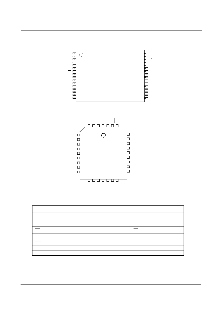
4. PIN CONFIGURATIONS
4.1 32-pin TSOP I
4.2 32-pin PLCC
4.3 Pin Description
Symbol Pin
Name
Functions
A0~A18 Address
Input
To provide memory addresses.
DQ0~DQ7 Data
Input/Output
To output data when Read and receive data when Write.
The outputs are in tri-state when OE or CE is high.
CE
Chip Enable
To activate the device when CE is low.
OE
Output Enable
To gate the data output buffers.
WE
Write Enable
To control the Write operations.
V
CC
Power Supply
To provide power
GND Ground
5
6
7
8
9
10
11
12
13
A7
A6
A5
A4
A3
A2
A1
A0
DQ0
2 9
2 8
2 7
2 6
2 5
2 4
2 3
2 2
2 1
A14
A13
A8
A9
A11
OE
A10
C E
DQ7
DQ
6
DQ
5
DQ
4
DQ
3
GN
D
DQ
2
DQ
1
32 31 30
A1
7
WE
V
CC
A1
8
A1
6
A1
5
A1
2
14 15 16 17 18 19 20
4 3 2 1
1
2
3
4
5
6
7
8
9
10
11
12
13
14
15
16
A11
A9
A8
A13
A14
A17
WE
VCC
A18
A16
A15
A12
A7
A6
A5
A4
32
31
30
29
28
27
26
25
24
23
22
21
20
19
18
17
OE
A10
CE
DQ 7
DQ 6
DQ 5
DQ 4
DQ 3
G ND
DQ 2
DQ 1
DQ 0
A0
A1
A2
A3
F49L040A
EFST
F49L040A
Elite Flash Storage Technology Inc.
Publication Date : Apr. 2005
Revision: 1.0 5/41
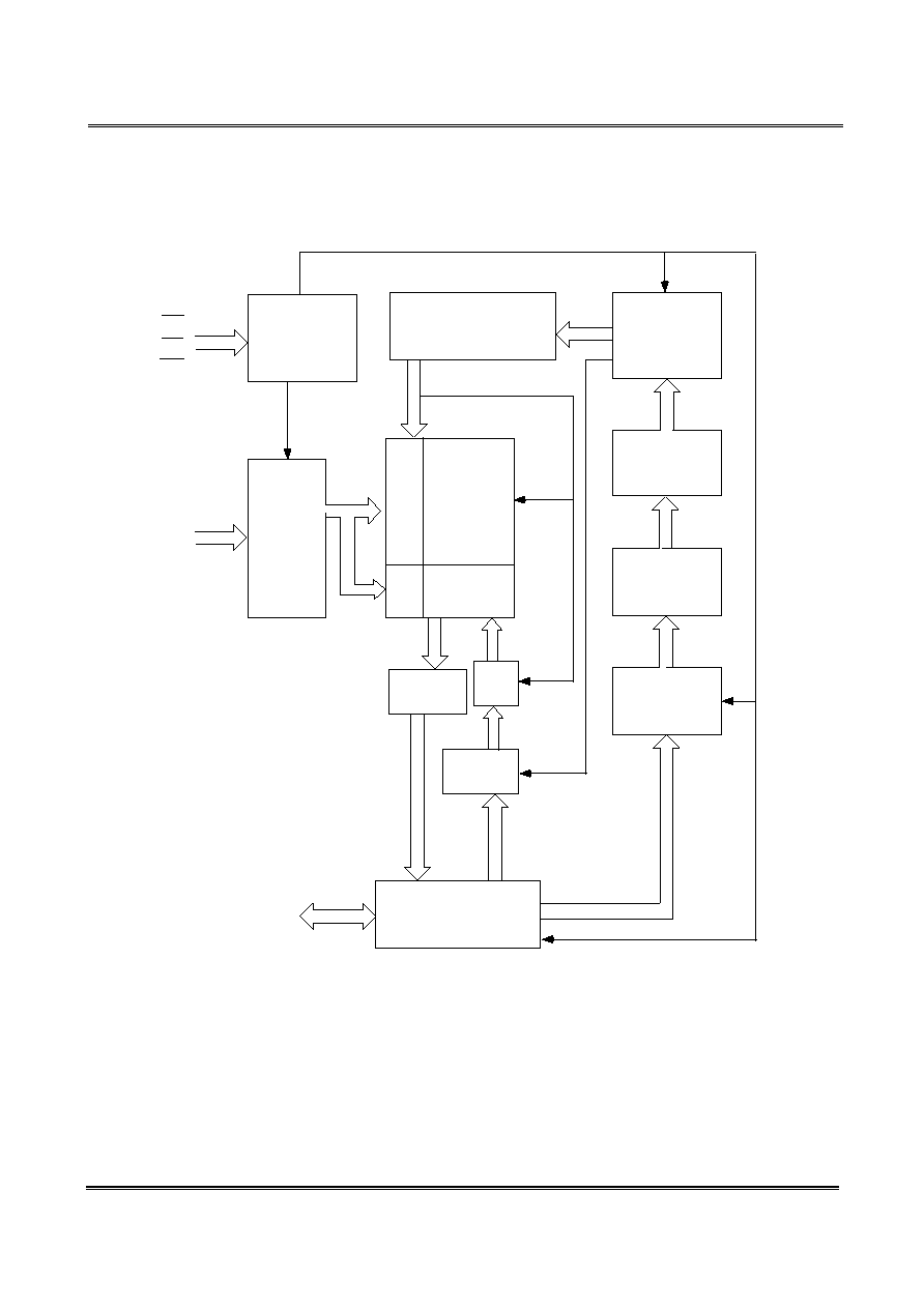
7. FUNCTIONAL DESCRIPTION
7.1 Device operation
This section describes the requirements and use
of the device bus operations, which are initiated
through the internal command register. The
register is composed of latches that store the
command, address and data information needed
to execute the command. The contents of the
register serve as inputs to the internal state
machine. The state machine outputs dictate the
function of the device. The F49L040A features
various bus operations as Table 2.
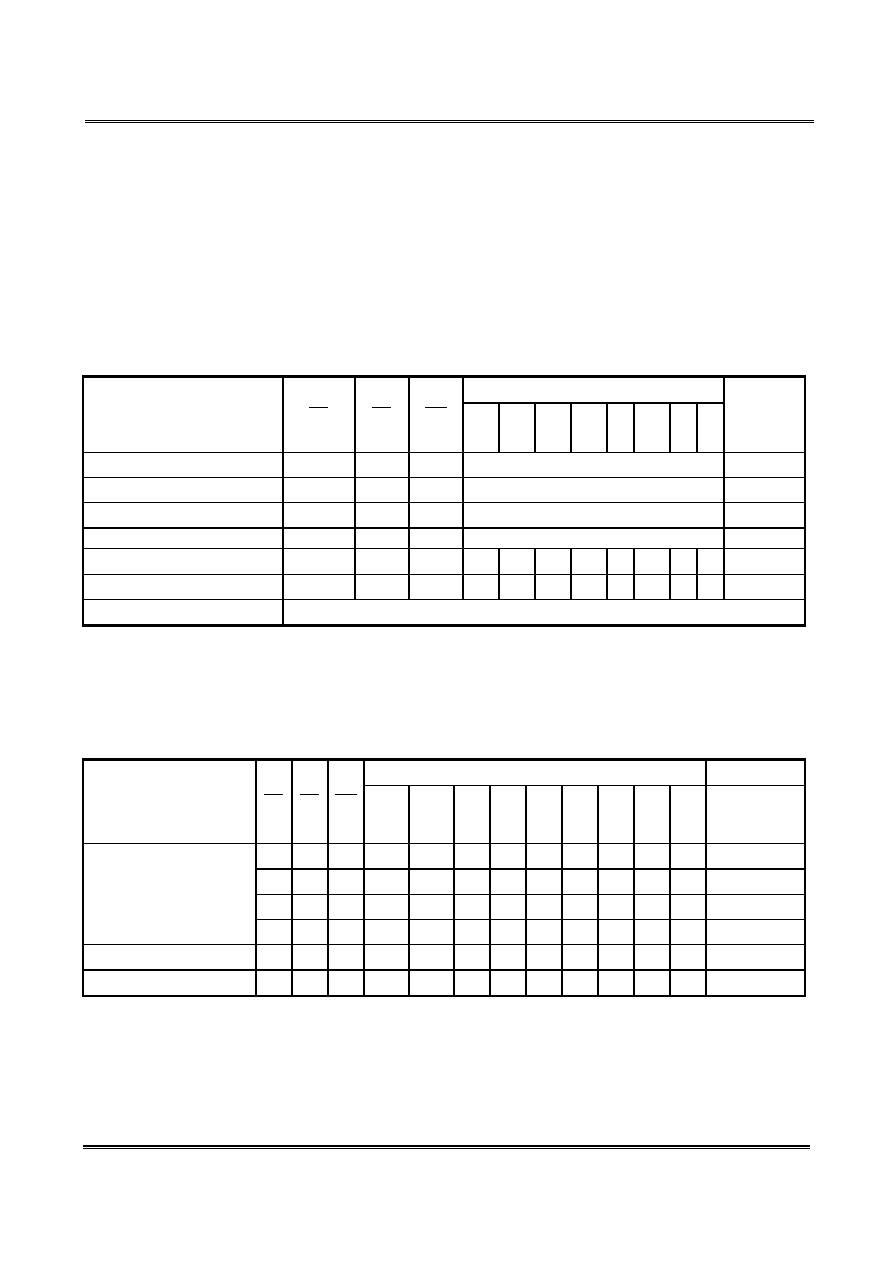
Table 2. F49L040A Operation Modes Selection
ADDRESS
DESCRIPTION
CE
OE
WE
A18
|
A13
A12
|
A10
A9
A8
|
A7
A6
A5
|
A2
A1 A0
DQ0~DQ7
Read L
L
H
AIN
Dout
Write L
H
L
AIN
DIN
Output Disable
L
H
H
X
High Z
Standby
H
X X
X
High
Z
Sector Protect(2)
L
H
L
SA
X
V
ID
X
L
X H L
DIN
Sector Unprotect(2)
L
H
L
SA
X
V
ID
X
H
X H L
DIN
Auto-select
See Table 3
Notes:
1.
L= Logic Low = V
IL
, H= Logic High = V
IH
, X= Don't Care, SA= Sector Address, V
ID
=11.5V to 12.5V.
AIN= Address In, DIN = Data In, Dout = Data Out.
2. The sector protect and unprotect functions may also be implemented via programming equipment.
Table 3. F49L040A Auto-Select Mode (High Voltage Method)
ADDRESS DQ0~DQ7
DESCRIPTION
CE OE WE A18
|
A13
A12
|
A10
A9
A8
|
A4
A6
A3
A2
A1 A0
L L H X X V
ID
X
X
L H
L L
7FH
L L H X X V
ID
X
X
H
L L L
7FH
L L H X X V
ID
X
X
H
H
L L
7FH
(Manufacturer ID:EFST)
L L H X X V
ID
X
X
L L L L
8CH
(Device ID: F49L040A)
L L H X X V
ID
X
X
X
X
L
H
4FH
Sector Protection Verify
L
L
H
SA
X
V
ID
X
L X
X
H L Code(2)
Notes :
1.Manufacturer and device codes may also be accessed via the software command sequence in Table 4.
2. Code=00H means unprotected.
Code =01H means protected.