OUTPUT SPECIFICATIONS
Output power
5 Watts max
Voltage accuracy Full load and nominal Vin
Ī 2%
Minimum load (Note 1)
10% of FL
Line regulation LL to HL at Full Load
Ī 0.2%
Load regulation
10% to 100% FL Single
Dual
Ī 0.2%
Ī 1%
Cross regulation (Dual) Asymmetrical load 25% / 100% FL
Ī 5%
Ripple and noise 20MHz bandwidth
50mVp-p
Temperature coefficient
I
0.02% / ļC, max
Transient response
recovery time
25% load step change
FL to 1/2 FL
I
1% error band
Single 200uS
Dual 200uS
Over load protection
% of FL at nominal input
170% typ
Short circuit protection
Continuous, automatics recovery
INPUT SPECIFICATIONS
Input voltage range
FDC05
FDC05-W
12V nominal input
24V nominal input
48V nominal input
24V nominal input
48V nominal input
9 ≠ 18VDC
18 ≠ 36VDC
36 ≠ 75VDC
9 ≠ 36VDC
18 ≠ 75VDC
Input filter
Pi
type
Input surge voltage
100mS max
12V input
24V input
48V input
36VDC
50VDC
100VDC
Input reflected ripple (Note 2)
Nominal Vin and full load
20mAp-p
Start up time
Nominal Vin and constant resistor load
600mS typ
Remote ON/OFF (Note 3)
(Positive logic)
(Negative logic)
Remote off input current
DC-DC ON
DC-DC OFF
DC-DC ON
DC-DC OFF
Nominal Vin
Open or 3.5V < Vr < 12V
Short or 0V < Vr < 1.2V
Short or 0V < Vr < 1.2V
Open or 3.5V < Vr < 12V
2.5mA
GENERAL SPECIFICATIONS
Efficiency See
table
Isolation Voltage Input to Output to Case
1600VDC, min
Isolation resistance
10
9
ohms, min
Isolation capacitance
300pF, max
Switching frequency
Standard
"W" series
300KHz, typ
200KHz, typ
Approvals and standard
IEC60950, UL1950, EN60950
Case material
Nickel-coated copper
Base material
Non-conducted black plastic
Potting material
Epoxy (UL94-V0)
Dimensions
2.00 X 1.00 X 0.40 Inch
(50.8 X 25.4 X 10.2 mm)
Weight
27g (0.95oz)
MTBF (Note 4)
3.145 x 10
6
hrs
ENVIRONMENTAL SPECIFICATIONS
Operating temperature range
(Reference derating curve)
Standard
M1 (Note 5)
M2 (W series)
-25ļC ~ +85ļC (with derating)
-40ļC ~ +85ļC (non-derating)
-40ļC ~ +85ļC (with derating)
Maximum case temperature
+100ļC
Storage temperature range
-55ļC ~ +105ļC
Thermal impedance (Note 6)
Nature convection
Nature convection with heat-sink
12ļC/watt
10ļC/watt
Thermal shock
MIL-STD-810D
Vibration
10~55Hz, 2G, 30minutes along X,Y and Z
Relative humidity
5% to 95% RH
EMC CHARACTERISTICS
Conducted emissions
EN55022
Level A
Radiated emissions
EN55022
Level A
ESD EN61000-4-2
Perf.
Criteria2
Radiated immunity
EN61000-4-3
Perf. Criteria2
Fast transient
EN61000-4-4
Perf. Criteria2
Surge EN61000-4-5
Perf.
Criteria2
Conducted immunity
EN61000-4-6
Perf. Criteria2
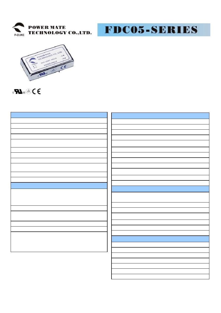
The FDC05 and FDC05-W series offer 5 watts of output power from a 2 x 1 x 0.4 inch
package without derating to 71ļC ambient temperature. FDC05 series have 2:1 wide input
voltage of 9-18, 18-36 and 36-75VDC. FDC05-W series have 4:1 ultra wide input voltage of
9-36 and 18-75VDC. The FDC05 and FDC05-W features 1600VDC of isolation, short-circuit
protection, as well as six sided shielding. The safety approve with EN60950 and UL1950. All
models are particularly suited to telecommunications, industrial, mobile telecom and test
equipment applications. According the extended operation temperature range, there are
"M1" and "M2" version for special application.
T E C H N I C A L S P E C I F I C A T I O N
All specifications are typical at nominal input, full load and 25ļC otherwise noted
UL E193009
TUV R3-50007936
CB JPTUV-003641
CE MARK
∑
5 WATTS OUTPUT POWER
∑
2:1 AND 4:1 WIDE INPUT VOLTAGE RANGE
∑
INTERNATIONAL SAFETY STANDARD APPROVAL
∑
SIX-SIDED CONTINUOUS SHIELD
∑
HIGH EFFICIENCY UP TO 83%
∑
STANDARD 2" X 1" X 0.4" PACKAGE
∑
FIXED SWITCHING FREQUENCY
Model
Number
Input
Range
Output
Voltage
Output
Current
Input
Current
(7)
Eff
(8)
(%)
Capacitor
Load max
(9)
FDC05-12S33
9 ≠ 18 VDC
3.3 VDC
1000mA
387mA
75
3700uF
FDC05-12S05
9 ≠ 18 VDC
5 VDC
1000mA
556mA
79 1700uF
FDC05-12S12
9 ≠ 18 VDC
12 VDC
470mA
610mA
81
290uF
FDC05-12S15
9 ≠ 18 VDC
15 VDC
400mA
658mA
80
188uF
FDC05-12D05
9 ≠ 18 VDC
Ī 5 VDC
Ī 500mA
595mA
74
Ī 850uF
FDC05-12D12
9 ≠ 18 VDC
Ī 12 VDC
Ī 230mA
597mA
81
Ī 140uF
FDC05-12D15
9 ≠ 18 VDC
Ī 15 VDC
Ī 190mA
609mA
82
Ī 47uF
FDC05-24S33 (W)
18 ≠ 36 (9 ≠ 36) VDC
3.3 VDC
1000mA
199 (196mA)
73 (74)
3700uF
FDC05-24S05 (W)
18 ≠ 36 (9 ≠ 36) VDC
5 VDC
1000mA
282 (274mA)
78 (80)
1700uF
FDC05-24S12 (W)
18 ≠ 36 (9 ≠ 36) VDC
12 VDC
470mA
305 (301mA)
81 (82)
290uF
FDC05-24S15 (W)
18 ≠ 36 (9 ≠ 36) VDC
15 VDC
400mA
325 (325mA)
81 (81)
188uF
FDC05-24D05 (W)
18 ≠ 36 (9 ≠ 36) VDC
Ī 5 VDC
Ī 500mA
289 (289mA)
76 (76)
Ī 850uF
FDC05-24D12 (W)
18 ≠ 36 (9 ≠ 36) VDC
Ī 12 VDC
Ī 230mA
295 (295mA)
82 (82)
Ī 140uF
FDC05-24D15 (W)
18 ≠ 36 (9 ≠ 36) VDC
Ī 15 VDC
Ī 190mA
308 (301mA)
81 (83)
Ī 47uF
FDC05-48S33 (W)
36 ≠ 75 (18 ≠ 75) VDC
3.3 VDC
1000mA
100 (100mA)
73 (73)
3700uF
FDC05-48S05 (W)
36 ≠ 75 (18 ≠ 75) VDC
5 VDC
1000mA
145 (149mA)
76 (74)
1700uF
FDC05-48S12 (W)
36 ≠ 75 (18 ≠ 75) VDC
12 VDC
470mA
151 (151mA)
82 (82)
290uF
FDC05-48S15 (W)
36 ≠ 75 (18 ≠ 75) VDC
15 VDC
400mA
160 (163mA)
82 (81)
188uF
FDC05-48D05 (W)
36 ≠ 75 (18 ≠ 75) VDC
Ī 5 VDC
Ī 500mA
149 (149mA)
74 (74)
Ī 850uF
FDC05-48D12 (W)
36 ≠ 75 (18 ≠ 75) VDC
Ī 12 VDC
Ī 230mA
149 (149mA)
81 (81)
Ī 140uF
FDC05-48D15 (W)
36 ≠ 75 (18 ≠ 75) VDC
Ī 15 VDC
Ī 190mA
154 (154mA)
81 (81)
Ī 47uF
PIN CONNECTION
PIN
SINGLE
DUAL OUTPUT
1
+ INPUT
+ INPUT
2
- INPUT
- INPUT
3
+ OUTPUT
+ OUTPUT
4
NO PIN
COMMON
5
- OUTPUT
- OUTPUT
6
CTRL (Option)
CTRL (Option)
1. All dimensions in Inches (mm)
2. Pin Pitch tolerance
I
0.014(0.35)
2
.
00(
50
.
8
)
0.40
(10.2)
0.40
(10.2)
0.50
(12.7)
1.00(25.4)
0.10(2.5)
0.20(5.1)
0.
8
0
(
2
0.
3)
0.
6
0
(
1
5.
2)
0.22(5.6)
0.40
(10.2)
D
I
A
.
0.
04
(
1
.
0
)
1 2
3
4
5
6
Bottom
View
Note
1.
The FDC05 (W) series required a minimum 10% loading on the output to maintain specified
regulation. Operation under no-load condition will not damage these devices, however they may not
meet all listed specification
2.
Simulated source impedance of 12uH. 12uH inductor on series with + Vin.
3.
The ON/OFF control is option function. There are positive logic and negative logic. The pin voltage is
referenced to negative input
To order positive logic ON-OFF control add the suffix-P (Ex: FDC05-24S05-P)
To order negative logic ON-OFF control add the suffix-N (Ex: FDC05-24S05-N)
4.
BELLCORE TR-NWT-000332. Case I: 50% Stress, Temperature at 40ļC.
(Ground fixed and controlled environment)
5. M1 version is more efficient, therefore, it can be operated in a more extensive temperature range than
standard and M2 version.
6.
Heat sink is optional and P/N: 7G-0020A.
7. Maximum value at nominal input voltage and full load of standard type.
8.
Typical value at nominal input voltage and full load.
9.
Test by minimum Vin and constant resistor load.
0.4
0.6
0.8
1.0
0.05 0.2
45
65
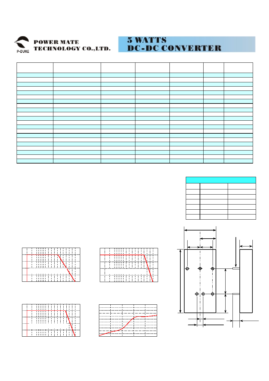
OUTPUT LOAD (A)
E
FFI
CIE
N
CY
(
%
)
FDC05-48S05
Efficiency VS Output load
82
81
80
79
78
77
76
75
70
50 60 70 80 90 100
-40 -25
0
-10
25
50
75
100
0
AMBIENT TEMPERATURE (ļC)
OU
TPU
T
PO
W
E
R
(
%
)
FDC05-48S05 Derating Curve
Nature convection
50 60 70 80 90 100
-40 -25
0
-10
25
50
75
100
0
AMBIENT TEMPERATURE (ļC)
O
U
TP
UT
P
O
W
E
R (
%
)
FDC05-48S05-M1 Derating Curve
Nature convection
50 60 70 80 90 100
-40 -25
0
-10
25
50
75
100
0
AMBIENT TEMPERATURE (ļC)
OU
T
P
U
T
P
O
W
E
R
(%
)
FDC05-48S05 Derating Curve
With HEAT-SINK (Note5)
Nature convection