OUTPUT SPECIFICATIONS
Output power
30
Watts max
Voltage accuracy Full load and nominal Vin Single/Dual
± 1%
Voltage adjustability
± 10%
Minimum load
Single/Dual
0%
Line regulation LL to HL at Full Load
Single
Dual
± 0.2%
± 0.5
Load regulation 10% to 100% FL
Single
Dual
± 0.5%
± 1%
Cross regulation (Dual) Asymmetrical load 25% / 100% FL
± 5%
Ripple and noise
20MHz bandwidth
(Measured with a 104pF/50V MLCC)
See table
Temperature coefficient
±
0.02% / ∫C, max
Transient response recovery time
25% load step change
300uS
Over voltage protection
Zener diode clamp
1.5V output
1.8V output
2.5V output
3.3V output
5V output
12V output
15V output
3.9V
3.9V
3.9V
3.9V
6.2V
15V
18V
Over load protection
% of FL at nominal input
150%,max
Short circuit protection
Hiccup, automatics recovery
INPUT SPECIFICATIONS
Input voltage range
12V nominal input
24V nominal input
48V nominal input
9 ≠ 18VDC
18 ≠ 36VDC
36 ≠ 75VDC
Under voltage lockout
12V input
24V input
48V input
DC-DC ON
DC-DC OFF
DC-DC ON
DC-DC OFF
DC-DC ON
DC-DC OFF
9VDC
8VDC
17.8VDC
16VDC
36VDC
33VDC
Input filter
L-C
type
Input voltage variation dv/dt
5V/ms,max
(Complies with ETS300 132 part 4.4)
Input surge voltage
100mS max
12V input
24V input
48V input
36VDC
50VDC
100VDC
Input reflected ripple
(Note1)
Nominal Vin and full load
30mAp-p
Start up time
Nominal Vin and
constant resistive load
Power up
Remote ON/OFF
25mS typ
25mS typ
Remote ON/OFF (Note 2)
(Positive logic)
Remote off input current
DC-DC ON
DC-DC OFF
Nominal Vin
Open or 3.5V < Vr < 12V
Short or 0V < Vr < 1.2V
2.5mA
GENERAL SPECIFICATIONS
Efficiency
See table
Isolation voltage
Input to Output
Input (Output) to Case
1600VDC, min
Isolation resistance
10
9
ohms, min
Isolation capacitance
1000pF, max
Switching frequency
300KHz, typ
Approvals and standard
IEC60950-1, UL60950-1, EN60950-1
Case material
Nickel-coated copper
Base material
Non-conductive black plastic
Potting material
Epoxy (UL94-V0)
Dimensions
2.00 X 1.60 X 0.40 Inch
(50.8 X 40.6 X 10.2 mm)
Weight
48g (1.69oz)
MTBF (Note 3)
1.535 x 10
6
hrs
ENVIRONMENTAL SPECIFICATIONS
Operating temperature range
-40∫C ~ +85∫C (with derating)
Maximum case temperature
100∫C
Storage temperature range
-55∫C ~ +105∫C
Over temperature protection
115∫C, typ
Thermal impedance (Note 4)
Nature convection
Nature convection with heat-sink
10∫C/Watt
8.24∫C/Watt
Thermal shock
MIL-STD-810D
Vibration
10~55Hz, 10G, 30minutes along X,Y and Z
Relative humidity
5% to 95% RH
EMC CHARACTERISTICS
(Note 5)
Conducted emissions
EN55022
Class A
Radiated emissions
EN55022
Class A
ESD
EN61000-4-2
Perf. Criteria B
Radiated immunity
EN61000-4-3
Perf. Criteria A
Fast transient
EN61000-4-4
Perf. Criteria B
Surge
EN61000-4-5
Perf. Criteria B
Conducted immunity
EN61000-4-6
Perf. Criteria A
The FEC30 series offer 30 Watts of output power from a 2 x 1.6 x 0.4 inch package.
The FEC30 series with 2:1 wide input voltage of 9-18VDC,18-36VDC and 36-75VDC
and features 1600VDC of isolation, short-circuit and over-voltage protection,as well
as six sided shielding. A safety approval to EN60950-1 and UL60950-1. All models are
particularly suited to telecommunications, industrial, mobile telecom and test
equipment applications.
T E C H N I C A L S P E C I F I C A T I O N
All specifications are typical at nominal input, full load and 25∫C otherwise noted
UL E193009
TUV
CB
CE MARK
∑
OFFER SINGLE AND DUAL OUTPUT
∑
30 WATTS MAXIMUM OUTPUT POWER
∑
2:1 WIDE INPUT VOLTAGE RANGE
∑
INTERNATIONAL SAFETY STANDARD APPROVAL
∑
SIX-SIDED CONTINUOUS SHIELD
∑
HIGH EFFICIENCY UP TO 90%
∑
STANDARD 2" x 1.6" x 0.4" PACKAGE
∑
FIXED SWITCHING FREQUENCY
VER:04 1 / 3
VER:04 2 / 3
Model
Number
Input
Range
Output
Voltage
Output
Current
Output
Ripple&Noise
Input
Current
(6)
Eff
(7)
(%)
Capacitor
(8)
Load max
FEC30-12S1P5
9-18 VDC
1.5 VDC
6000mA
50mVp-p
1014mA
78
85800uF
FEC30-12S1P8
9-18 VDC
1.8VDC
6000mA
50mVp-p
1169mA
81
65000uF
FEC30-12S2P5 9-18
VDC 2.5VDC
6000mA
50mVp-p
1582mA
83
33000uF
FEC30-12S3P3
9-18 VDC
3.3 VDC
6000mA
50mVp-p
2037mA
85
19500uF
FEC30-12S05
9-18 VDC
5 VDC
6000mA
50mVp-p
3012mA
87
10200uF
FEC30-12S12
9-18 VDC
12 VDC
2500mA
75 mVp-p
2976mA
88
3240uF
FEC30-12S15
9-18 VDC
15VDC
2000mA
75 mVp-p
2976mA
88
1100uF
FEC30-12D12
9-18 VDC
±
12 VDC
±1250mA
100 mVp-p
3012mA
87
±1020uF
FEC30-12D15 9-18
VDC
±
15 VDC
±1000mA 100
mVp-p
3012mA
87 ±675uF
FEC30-24S1P5
18 ≠ 36 VDC
1.5 VDC
6000mA
50mVp-p
493mA
80
85800uF
FEC30-24S1P8
18 ≠ 36 VDC
1.8 VDC
6000mA
50mVp-p
580mA
82
65000uF
FEC30-24S2P5
18 ≠ 36 VDC
2.5 VDC
6000mA
50mVp-p
780mA
84
33000uF
FEC30-24S3P3
18 ≠ 36 VDC
3.3 VDC
6000mA
50mVp-p
1010mA
86
19500uF
FEC30-24S05
18 ≠ 36 VDC
5 VDC
6000mA
50mVp-p
1490mA
88
10200uF
FEC30-24S12
18 ≠ 36 VDC
12 VDC
2500mA
75 mVp-p
1470mA
89
3300uF
FEC30-24S15
18 ≠ 36 VDC
15 VDC
2000mA
75 mVp-p
1470mA
89
1100uF
FEC30-24D12
18 ≠ 36 VDC
±
12 VDC
±1250mA
100 mVp-p
1488mA
88
±1020uF
FEC30-24D15
18 ≠ 36 VDC
±
15 VDC
±1000mA
100 mVp-p
1488mA
88
±675uF
FEC30-48S1P5
36 ≠ 75 VDC
1.5 VDC
6000mA
50mVp-p
244mA
81
85800uF
FEC30-48S1P8
36 ≠ 75 VDC
1.8 VDC
6000mA
50mVp-p
290mA
83
65000uF
FEC30-48S2P5
36 ≠ 75 VDC
2.5 VDC
6000mA
50mVp-p
390mA
85
33000uF
FEC30-48S3P3
36 ≠ 75 VDC
3.3 VDC
6000mA
50mVp-p
500mA
87
19500uF
FEC30-48S05
36 ≠ 75 VDC
5 VDC
6000mA
50mVp-p
740mA
89
10200uF
FEC30-48S12
36 ≠ 75 VDC
12 VDC
2500mA
75 mVp-p
730mA
90
3300uF
FEC30-48S15
36 ≠ 75 VDC
15 VDC
2000mA
75 mVp-p
730mA
90
1100uF
FEC30-48D12
36 ≠ 75 VDC
±
12 VDC
±1250mA
100 mVp-p
744mA
88
±1020uF
FEC30-48D15
36 ≠ 75 VDC
±
15 VDC
±1000mA 100
mVp-p
744mA
88 ±675uF
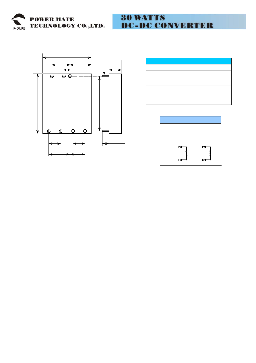
Note
1.
Please add an external filter at converter input terminals when measuring input
reflected ripple, as figure 1.
L: Simulated source impedance of 12uH.
C: Nippon chemi-con KMF series, 220
F/100V.
2.
The ON/OFF control pin voltage is referenced to negative input
3.
BELLCORE TR-NWT-000332. Case I: 50% Stress, Temperature at 40∫C. (Ground
fixed and controlled environment)
4.
Heat sink is optional and P/N: 7G-0011A.
5.
An external filter capacitor is required for
EMC testing
. The capacitor should be
capable of handing 1A ripple current for 12V/24V/48V models. Power mate suggest:
C: Nippon chemi-con KMF series, 220
F/100V, ESR 90m
.
6.
Maximum value at nominal input voltage and full load.
7.
Typical value at nominal input voltage and full load.
8.
Test by minimum Vin and constant resistive load.
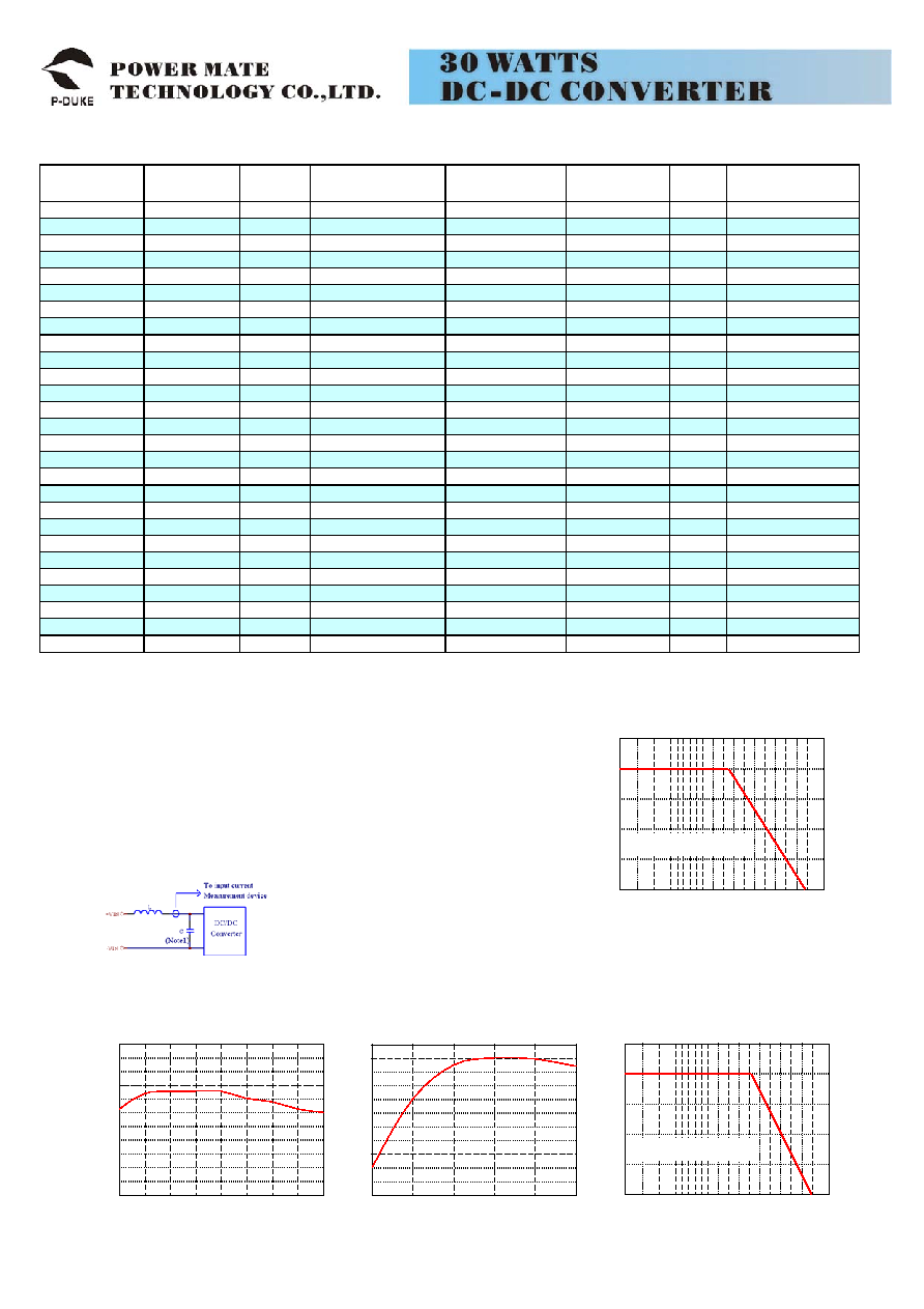
50 60 70 80 90 100
-40 -25
0
-10
25
50
75
100
0
AMBIENT TEMPERATURE (∫C)
OUTPUT
POWER (%)
FEC30-48S05
Derating Curve without Heat-Sink
Nature convection
50 60 70 80 90 100
-40 -25
0
-10
25
50
75
100
0
AMBIENT TEMPERATURE (∫C)
OUTPUT
POWER (%)
FEC30-48S05 (Note 5)
Derating Curve with Heat-Sink
Nature convection
60 65
70 75
36 50
40
82
83
INPUT VOLTAGE (V)
EFFICIENCY
(%)
FEC30-48S05
Efficiency VS Input voltage
92
91
90
89
88
87
86
85
84
45 55
3
4
5
6
1 2
74
76
OUTPUT LOAD (A)
EFFICIENCY
(%)
FEC30-48S05
Efficiency VS Output load
90
89
88
87
86
85
84
80
78
Figure 1