OUTPUT SPECIFICATIONS
Output power
40 Watts max
Voltage accuracy FL and nominal Vin
Single / Dual
Triple Main
Auxiliary
± 1%
± 1%
± 5%
Voltage adjustability (Note 1)
Single output only
± 10%
Minimum load (Note 2)
Single and Dual Positive
Dual and Triple
0%
10% of FL
Line regulation LL to HL at Full Load
Single/Dual
Triple(main)
Triple(auxiliary)
± 0.5%
± 1%
± 5%
Load regulation
(Note 3)
10% to 100% FL
Single
Dual
Triple Main
Auxiliary
± 0.5%
± 1%
± 2%
± 5%
Load cross regulation
(Note 4)
Triple(main)
Dual/Triple(auxiliary)
± 1%
± 5%
Ripple and noise
(Note 5)
20MHz bandwidth
(Measured with a 104pF/50V MLCC)
See table
Temperature coefficient
±
0.02% / ∫C, max
Transient response recovery time
25% load step change
250uS
Over voltage protection
Zener diode clamp
1.5V output
1.8V output
2.5V output
3.3V output
5V output
12V output
15V output
3.9V
3.9V
3.9V
3.9V
6.2V
15V
18V
Over load protection
% of FL at nominal input
150% max
Short circuit protection
Hiccup, automatics recovery
INPUT SPECIFICATIONS
Input voltage range
12V nominal inpu
24V nominal input
48V nominal input
9 ≠ 18VDC
18 ≠ 36VDC
36 ≠ 75VDC
Under voltage lockout
12V input
24V input
48V input
DC-DC ON
DC-DC OFF
DC-DC ON
DC-DC OFF
DC-DC ON
DC-DC OFF
9VDC
8VDC
17.8VDC
16VDC
36VDC
34VDC
Input filter
L-C
type
Input voltage variation dv/dt
5V/ms,max
(Complies with ETS300 132 part 4.4)
Input surge voltage
100mS max
24V input
48V input
50VDC
100VDC
Input reflected ripple (Note 6)
Nominal Vin and full load
40mAp-p
Start up time
Nominal Vin and
constant resistive load
Powe up
Remote ON/OFF
25mS typ
25mS typ
Remote ON/OFF (Note 7)
Remote off input current
DC-DC ON
DC-DC OFF
Nominal Vin
Open or 3.5V < Vr < 12V
Short or 0V < Vr < 1.2V
2.5mA
GENERAL SPECIFICATIONS
Efficiency
See table
Isolation voltage
Input to Output
Input(Output) to Case
1600VDC, min
1600VDC, min
Isolation resistance
10
9
ohms, min
Isolation capacitance
1000pF, max
Switching frequency (Note 8)
300KHz, typ
Approvals and standard
IEC60950-1, UL60950-1, EN60950-1
Case material
Nickel-coated copper
Base material
Non-conductive black FR4
Potting material
Epoxy (UL94-V0)
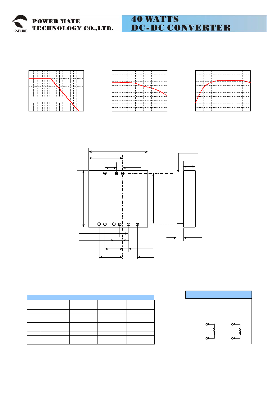
Dimensions
2.00 X 2.00 X 0.40 Inch
(50.8 X 50.8 X 10.2 mm)
Weight
60g (2.11oz)
MTBF (Note 9)
1.398 x 10
6
hrs
ENVIRONMENTAL SPECIFICATIONS
Operating temperature range
-40∫C ~ +85∫C (with derating)
Maximum case temperature
+100∫C
Storage temperature range
-55∫C ~ +105∫C
Over temperature protection
115∫C, typ
Thermal impedance
(Note 10)
Nature convection
Heat-sink with 20LFM
Heat-sink with 500LFM
9.2∫C/Watt
8.5∫C/Watt
2.8∫C/Watt
Thermal shock
MIL-STD-810D
Vibration
10~55Hz,10G, 30minutes along X,Y and Z
Relative humidity
5% to 95% RH
EMC CHARACTERISTICS
(Note 11)
Conducted emissions
EN55022
Class A
Radiated emissions
EN55022
Class A
ESD
EN61000-4-2
Perf. Criteria B
Radiated immunity
EN61000-4-3
Perf. Criteria A
Fast transient
EN61000-4-4
Perf. Criteria B
Surge
EN61000-4-5
Perf. Criteria B
Conducted immunity
EN61000-4-6
Perf. Criteria A
The FEC40 series offer 40 watts of output power from a 2 x 2 x 0.4 inch package. The FEC40 series
with 2:1 wide input voltage of 9-18VDC,18-36VDC and 36-75VDC and features 1600VDC of
isolation, short-circuit and over-voltage protection, as well as six sided shielding. All models are
particularly suited to telecommunications, industrial, mobile telecom and test equipment applications.
T E C H N I C A L S P E C I F I C A T I O N
All specifications are typical at nominal input, full load and 25∫C otherwise noted
UL E193009
TUV
CB
CE MARK
Patent No.144566
∑
OFFER SINGLE, DUAL,DUAL POSITIVE(TOTAL OUTPUT
CURRENT 8A) AND TRIPLE OUTPUT
∑
40 WATTS MAXIMUM OUTPUT POWER
∑
2:1 WIDE INPUT VOLTAGE RANGE
∑
INTERNATIONAL SAFETY STANDARD APPROVAL
∑
SIX-SIDED CONTINUOUS SHIELD
∑
HIGH EFFICIENCY UP TO 90%
∑
STANDARD 2" x 2" x 0.4" PACKAGE
∑
FIXED SWITCHING FREQUENCY
VER:05 1 / 3
Note
1.
Maximum output deviation is 10% inclusive of remote sense and trim. If remote sense is not being used, the +Vsense should be
connected to its corresponding +OUTPUT and likewise the sense should be connected to its corresponding ≠OUTPUT.
2.
The dual and triple output required a minimum 10% loading on the output to maintain specified regulation. Operation under no-load
condition will not damage these devices, however they may not meet all listed specification
3.
Load regulation for triple output:
Main output(V1):10 to 100% with 10% to 100% balanced on auxiliaries.
Auxiliary outputs(V2 and V3):10% to 100% balanced on all outputs.
4.
Cross regulation for dual output: asymmetrical load 25% / 100% FL
Cross regulation for triple output:
Main output 100% load, auxiliary 100%,other auxiliary25% to 100%.
Auxiliary outputs(V2 and V3):main output 100% load, auxiliary 100%, other auxiliary 25% to 100% or main output 25%,auxiliary
25%,other auxiliary 25% to 100%.
5.
The models of FEC40-XXD3305 are specified with a 1uF ceramic output capacitors.
6.
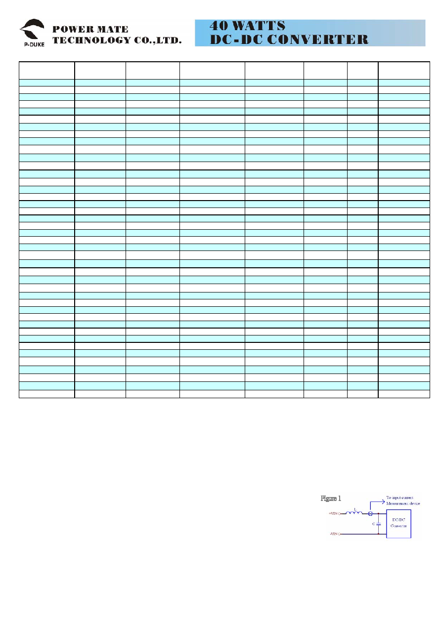
Please add an external filter at converter input terminals when measuring input reflected ripple, as
Figure 1. L : Simulated source impedance of 12uH.
C: Nippon chemi-con KMF series, 220
F/100V
7.
The ON/OFF control pin voltage is referenced to negative input.
8.
Switching frequency for dual output:
master (5Vo) 300KHz slave (3.3Vo) 500KHz
9.
BELLCORE TR-NWT-000332. Case I: 50% Stress, Temperature at 40∫C. (Ground fixed and controlled environment).
10. Heat sink is optional and P/N
7G-0026A.
11. An external filter capacitor is required for
EMC testing
. The capacitor should be capable
of handing 1A ripple current for 12V/24V/48V models. Power mate suggest: Nippon chemi-con KMF
series, 220
F/100V, ESR 90m
.
12. Any condition of dual output (3.3V/5V) rated Iout current, not to exceed 8A of total output currents. The product safety approval pending..
13. Maximum value at nominal input voltage and full load.
14. Typical value at nominal input voltage and full load.
15. Test by minimum Vin and constant resistive load.
Model
Number
Input
Range
Output
Voltage
Output
Current
Output
Ripple & Noise
Input
Current
(13)
Eff
(14)
(%)
Capacitor
(15)
Load max
FEC40-12S1P5
9 ≠ 18 VDC
1.5 VDC
8000mA
50mVp-p
1250mA
84
45000uF
FEC40-12S1P8
9 ≠ 18 VDC
1.8 VDC
8000mA
50mVp-p
1538mA
82
37700uF
FEC40-12S2P5
9 ≠ 18 VDC
2.5 VDC
8000mA
50mVp-p
2083mA
84
27000uF
FEC40-12S3P3
9 ≠ 18 VDC
3.3 VDC
8000mA
50mVp-p
2683mA
86
21000uF
FEC40-12S05
9 ≠ 18 VDC
5 VDC
8000mA
50mVp-p
4065mA
86
13600uF
FEC40-12S12
9 ≠ 18 VDC
12 VDC
3333mA
75mVp-p
4065mA
86
2360uF
FEC40-12S15
9 ≠ 18 VDC
15 VDC
2666mA
75mVp-p
4015mA
87
1510uF
FEC40-12D12
9 ≠ 18 VDC
± 12 VDC
± 1800mA
120mVp-p
4444mA
85
± 1200uF
FEC40-12D15
9 ≠ 18 VDC
± 15 VDC
± 1400mA
150mVp-p
4321mA
85
± 750uF
FEC40-12D3305
9 ≠ 18 VDC
3.3 / 5 VDC
4A / 4A (total 8A)
(12)
100mVp-p
3416mA
85
11000 / 6800uF
FEC40-12T3312
9 ≠ 18 VDC
3.3 /
±
12 VDC
6000mA /
±
400mA
50 / 75mVp-p
3063mA
84
13000 /
±
330uF
FEC40-12T3315
9 ≠ 18 VDC
3.3 /
±
15 VDC
6000mA /
±
300mA
50 / 75mVp-p
3000mA
84
13000 /
±
110uF
FEC40-12T0512
9 ≠ 18 VDC
5 /
±
12 VDC
6000mA /
±
400mA
50 / 75mVp-p
4024mA
86
6800 /
±
330uF
FEC40-12T0515
9 ≠ 18 VDC
5 /
±
15 VDC
6000mA /
±
300mA
50 / 75mVp-p
3963mA
86
6800 /
±
110uF
FEC40-24S1P5
18 ≠ 36 VDC
1.5 VDC
8000mA
50mVp-p
649mA
81
45000uF
FEC40-24S1P8
18 ≠ 36 VDC
1.8 VDC
8000mA
50mVp-p
759mA
83
37700uF
FEC40-24S2P5
18 ≠ 36 VDC
2.5 VDC
8000mA
50mVp-p
1016mA
86
27000uF
FEC40-24S3P3
18 ≠ 36 VDC
3.3 VDC
8000mA
50mVp-p
1325mA
87
21000uF
FEC40-24S05
18 ≠ 36 VDC
5 VDC
8000mA
50mVp-p
1961mA
89
13600uF
FEC40-24S12
18 ≠ 36 VDC
12 VDC
3333mA
75mVp-p
2048mA
88
2360uF
FEC40-24S15
18 ≠ 36 VDC
15 VDC
2666mA
75mVp-p
1985mA
89
1510uF
FEC40-24D12
18 ≠ 36 VDC
± 12 VDC
± 1800mA
120mVp-p
2169mA
87
± 1200uF
FEC40-24D15
18 ≠ 36 VDC
± 15 VDC
± 1400mA
150mVp-p
2108mA
87
± 750uF
FEC40-24D3305
18 ≠ 36 VDC
3.3 / 5 VDC
4A / 4A (total 8A)
(12)
100mVp-p
1689mA
86
11000 / 6800uF
FEC40-24T3312
18 ≠ 36 VDC
3.3 /
±
12 VDC
6000mA /
±
400mA
50 / 75mVp-p
1512mA
85
13000 /
±
330uF
FEC40-24T3315
18 ≠ 36 VDC
3.3 /
±
15 VDC
6000mA /
±
300mA
50 / 75mVp-p
1481mA
85
13000 /
±
110uF
FEC40-24T0512
18 ≠ 36 VDC
5 /
±
12 VDC
6000mA /
±
400mA
50 / 75mVp-p
1989mA
87
6800 /
±
330uF
FEC40-24T0515
18 ≠ 36 VDC
5 /
±
15 VDC
6000mA /
±
300mA
50 / 75mVp-p
1958mA
87
6800 /
±
110uF
FEC40-48S1P5
36 ≠ 75 VDC
1.5 VDC
8000mA
50mVp-p
321mA
82
45000uF
FEC40-48S1P8
36 ≠ 75 VDC
1.8 VDC
8000mA
50mVp-p
375mA
84
37700uF
FEC40-48S2P5
36 ≠ 75 VDC
2.5 VDC
8000mA
50mVp-p
508mA
86
27000uF
FEC40-48S3P3
36 ≠ 75 VDC
3.3 VDC
8000mA
50mVp-p
655mA
88
21000uF
FEC40-48S05
36 ≠ 75 VDC
5 VDC
8000mA
50mVp-p
969mA
90
13600uF
FEC40-48S12
36 ≠ 75 VDC
12 VDC
3333mA
75mVp-p
1000mA
89
2360uF
FEC40-48S15
36 ≠ 75 VDC
15 VDC
2666mA
75mVp-p
992mA
89
1510uF
FEC40-48D12
36 ≠ 75 VDC
± 12 VDC
± 1800mA
120mVp-p
1084mA
87
± 1200uF
FEC40-48D15
36 ≠ 75 VDC
± 15 VDC
± 1400mA
150mVp-p
1054mA
87
± 750uF
FEC40-48D3305
36 ≠ 75 VDC
3.3 / 5 VDC
4A / 4A (total 8A)
(12)
100mVp-p
823mA
88
11000 / 6800uF
FEC40-48T3312
36 ≠ 75 VDC
3.3 /
±
12 VDC
6000mA /
±
400mA
50 / 75mVp-p
747mA
86
13000 /
±
330uF
FEC40-48T3315
36 ≠ 75 VDC
3.3 /
±
15 VDC
6000mA /
±
300mA
50 / 75mVp-p
732mA
86
13000 /
±
110uF
FEC40-48T0512
36 ≠ 75 VDC
5 /
±
12 VDC
6000mA /
±
400mA
50 / 75mVp-p
982mA
88
6800 /
±
330uF
FEC40-48T0515
36 ≠ 75 VDC
5 /
±
15 VDC
6000mA /
±
300mA
50 / 75mVp-p
967mA
88
6800 /
±
110uF
VER:05 2 / 3