 | –≠–ª–µ–∫—Ç—Ä–æ–Ω–Ω—ã–π –∫–æ–º–ø–æ–Ω–µ–Ω—Ç: FM30C256 | –°–∫–∞—á–∞—Ç—å:  PDF PDF  ZIP ZIP |
This product conforms to specifications per the terms of the Ramtron
Ramtron International Corporation
standard warranty. Production processing does not necessarily in-
1850 Ramtron Drive, Colorado Springs, CO 80921
clude testing of all parameters.
(800) 545-FRAM, (719) 481-7000, Fax (719) 481-7058
www.ramtron.com
Rev 2.1
Dec. 2002
Page 1 of 18
FM30C256
256Kb Data Collector
Features
256K bit Ferroelectric Nonvolatile RAM
∑
Organized as 32,768 x 8 bits
∑
High Endurance 10 Billion (10
10
) Read/Writes
∑
10 year Data Retention
∑
NoDelayTM Writes
∑
Advanced High-Reliability Ferroelectric Process
Fast Two-wire Serial Interface
∑
Up to 1 MHz Maximum Bus Frequency
∑
Supports Legacy Timing for 100 kHz & 400 kHz
∑
Clock Registers Accessed via 2-wire Interface
Real-time Clock/Calendar
∑
Backup Current under 1
µ
A
∑
Tracks Seconds through Centuries (BCD format)
∑
Tracks Leap Years through 2099
∑
Uses Standard 32.768 kHz Crystal (6pF)
∑
Software Calibration
System Supervisor
∑
Active-low Reset Output for V
DD
Out-of-Tolerance
∑
Tamper Detect Input with Battery Backup and
Time Stamp
Description
The FM30C256 is a 256-kilobit data collection
subsystem including nonvolatile RAM, timekeeping,
CPU supervisor, and system tamper detection. Non-
volatile RAM is provided by FRAM technology,
which is ideal for collection data and requires no
battery backup for nonvolatile storage. In other
respects, it provides the same features as SRAM.
FRAM performs write operations at bus speed with
no write delays. Write cycles can be continuous
without block limitations. In addition, it offers much
higher write endurance than other nonvolatile
memories. The FM30C256 supports up to 10
10
read/write cycles.
The FM30C256 also includes timekeeping with
external battery backup. The timekeeper consists of
registers that represent time and date information in
BCD format. The clock includes a calibration mode
that allows a software adjustment for timekeeping
accuracy.
To maintain system data integrity, the FM30C256
provides a reset signal asserted when VDD is out of
tolerance. /RST remains active for 100 ms after VDD
returns to proper levels. The FM30C256 also
provides a battery-backed tamper detect circuit that
records a rising edge on the TIN input. A battery-
backed flag is set when the event occurs, but can only
be cleared by software.
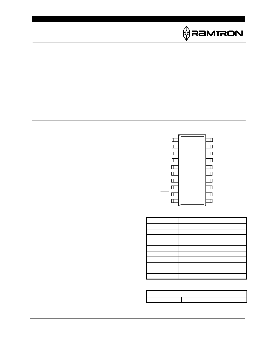
The FM30C256 is provided in a 20-pin SOIC
package and is guaranteed over an industrial
temperature range of ≠40∞C to +85∞C.
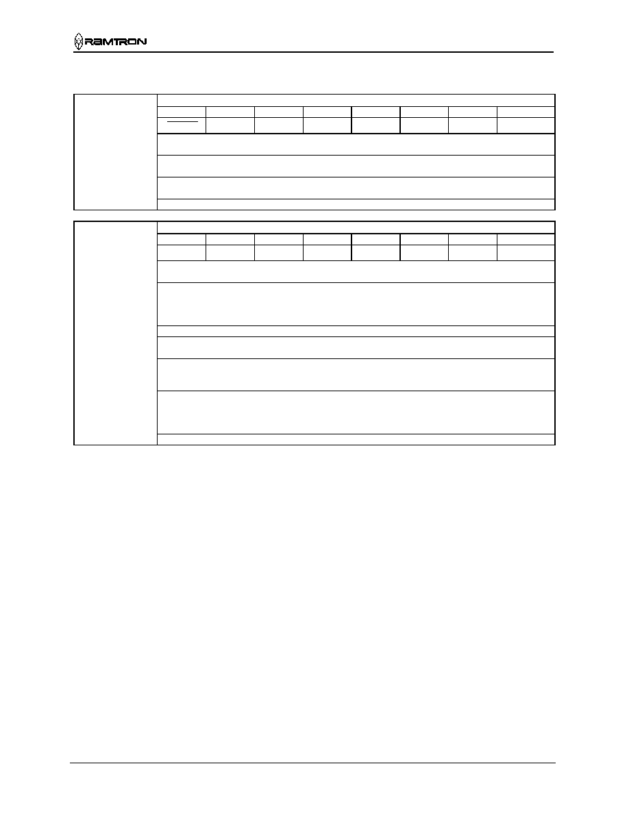
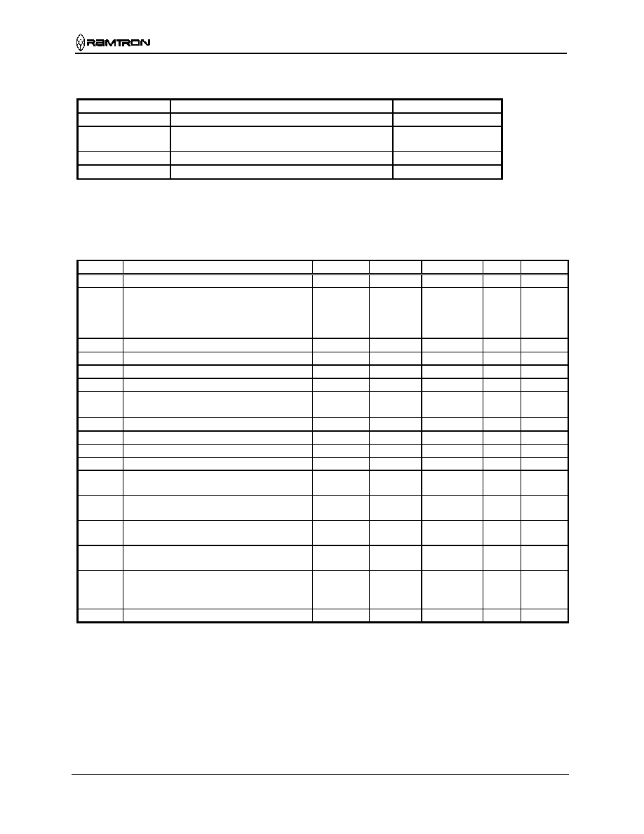
Pin Configuration
Pin Names
Function
TIN
Tamper Detect input
A0-A2 Device
Select
inputs
CAL
Clock Calibration output
/RST Reset
Output
X1, X2
Crystal Connections
SDA Serial
Data
SCL Serial
Clock
VDD Supply
Voltage
5V
VBAK Battery-Backup
input
VSS Ground
Ordering Information
FM30C256-S 20-pin
SOIC
VDD
VBAK
SCL
SDA
VSS
X1
X2
CAL
TIN
NC
NC
NC
NC
RST
NC
A0
A1
A2
NC
NC
1
2
3
4
5
6
7
8
9
10
20
19
18
17
16
15
14
13
12
11
FM30C256
Rev 2.1
Dec. 2002
Page 2 of 18
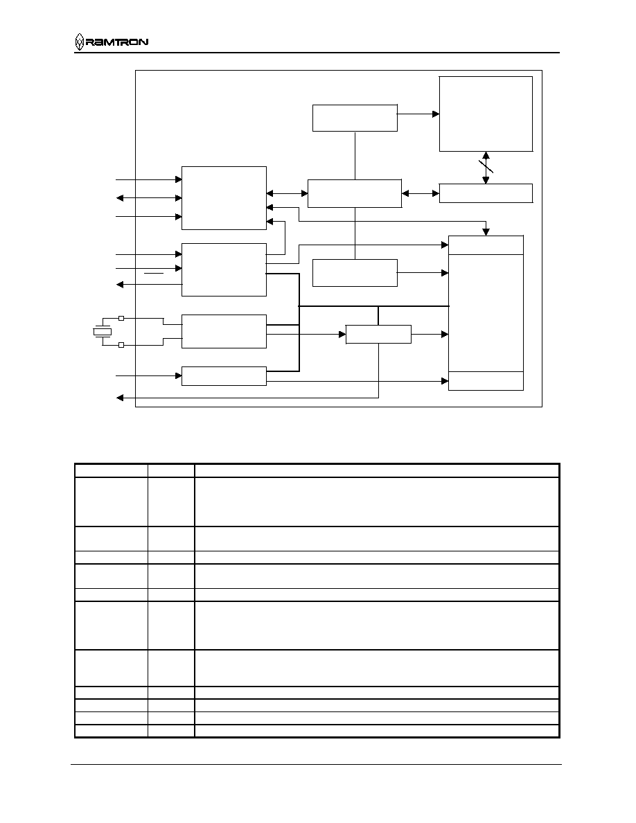
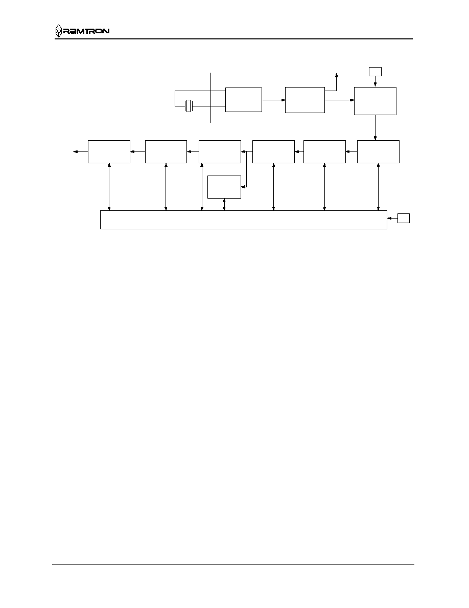
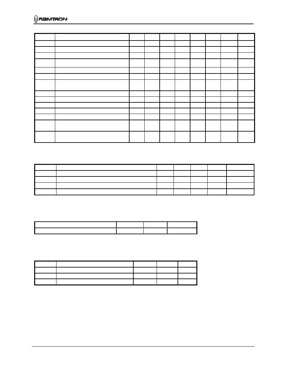
Figure 1. Block Diagram
Pin Descriptions
Pin Name
Type
Pin Description
A2-A0
Input
Device select inputs are used to address the part on a serial bus. To select the device,
the address value on the three pins must match the corresponding bits contained in
the device address. Note that these are not address pins for read/write operations.
The address pins are pulled down internally.
TIN
Input
Tamper detect is a battery backed input that stores a 1 in the Flags/Control register
when it detects a rising edge on the TIN pin.
CAL
Output
512 Hz square-wave output for clock calibration
X1, X2
I/O
32.768 kHz crystal connection. When using an external oscillator source, use X2 as
the oscillator input and leave X1 floating.
/RST
Output
Active low reset output (open drain)
SDA
I/O
Serial Data Address. This is a bi-directional line for the two-wire interface. It is
open-drain and is intended to be wire-OR'd with other devices on the two-wire bus.
The input buffer incorporates a Schmitt trigger for noise immunity and the output
driver includes slope control for falling edges. A pull-up resistor is required.
SCL
Input
Serial Clock. The serial clock line for the two-wire interface. Data is clocked out of
the part on the falling edge, and in on the rising edge. The SCL input also
incorporates a Schmitt trigger input for noise immunity.
VBAK
Supply
Battery backup supply voltage (3V)
VDD Supply
Supply
Voltage
(5V)
VSS Supply
Ground
NC -
No
connect
Address Latch &
Counter
32K x 8
FRAM Array
RTC Address
Latch & Counter
Serial to Parallel
Converter
Data Latch
8
Protocol &
Device Select
Real-time Clock
Registers
Power Isolation
Tamper Flag
Counters
Power
Management
RTC Oscillator
Tamper Latch
Battery-backed power
CAL
TIN
X2
X1
RST
VBAK
VDD
SCL
SDA
A2-A0
32.768
kHz
FM30C256
Rev 2.1
Dec. 2002
Page 3 of 18
Overview
The FM30C256 data collector combines a 256Kb
serial nonvolatile RAM with a real-time clock (RTC),
a power monitor, and a tamper detect circuit. The
FM30C256 integrates these complementary but
distinct functions under a common interface in a
single package. Despite providing multiple interface
Ids as explained below, the product is a single
monolithic device.
The memory is organized as 32Kx8 of FRAM and is
accessed via a separate 2-wire device ID from the
remaining functions. This allows the user to preserve
addressing information when switching between
memory and RTC functions. Modularity in software
design is preserved as well.
The real-time clock function and the tamper detection
is accessed under its own 2-wire device ID. This
allows clock data to be read while maintaining the
last (most recently used) memory address in the other
device. The clock and tamper functions are controlled
by 9 registers that are backed up by the external
battery. Clock and tamper functions continue to
operate from battery power when V
DD
drops below
the battery voltage.
In addition to the software-controlled functions, the
FM30C256 also provides reset signal for an external
microcontroller host. This signal is asserted when
V
DD
drops below the specified trip point (V
TP
). It
remains asserted until V
DD
returns above V
TP
for the
hold-off period (t
RPU
). The power monitor has no
interaction with other software-controlled functions.
Any access to the device will be ignored when V
DD
<
V
TP
.
Memory Operation
When accessing the FM30C256, the user addresses
32,768 locations each with 8 data bits. These data bits
are shifted in and out serially. The 32,768 addresses
are accessed using the two-wire protocol, which
includes a slave address (to distinguish from other
non-memory devices), and an extended 16-bit
address. The decoder uses only the lower 15 bits for
accessing the memory. The upper address bit should
be set to 0 for compatibility with larger devices in the
future.
The memory is read or written at the speed of the
two-wire bus. The interface protocol is described
further below.
RTC Register Map
The interface to clock and tamper functions is via 9
address locations mapped to a separate 2-wire device
ID. The interface protocol is described below. The
registers contain timekeeping data, control bits, or
information flags. A short description of each register
follows. Detailed descriptions follow the register
summary section.
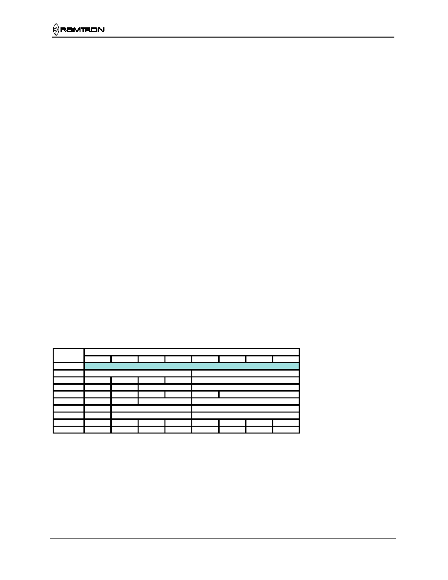
Register Map Summary Table
Data
Address
D7
D6
D5
D4
D3
D2
D1
D0
Function
Range
9-F
8
10 years
years
Years
00-99
7
0
0
0
10 mo
months
Month
1-12
6
0
0
10 date
date
Date
1-31
5
0
0
0
0
0
day
Day
1-7
4
0
0
10 hours
hours
Hours
0-23
3
0
10 minutes
minutes
Minutes
0-59
2
0
10 seconds
seconds
Seconds
0-59
1
/OSCEN
TSEN
CALS
CAL4
CAL3
CAL2
CAL1
CAL0
CAL/Control
0
Tamper
CF
reserved reserved
TST
CAL
W
R
Flags/Control
ILLEGAL ADDRESSES
FM30C256
Rev 2.1
Dec. 2002
Page 4 of 18
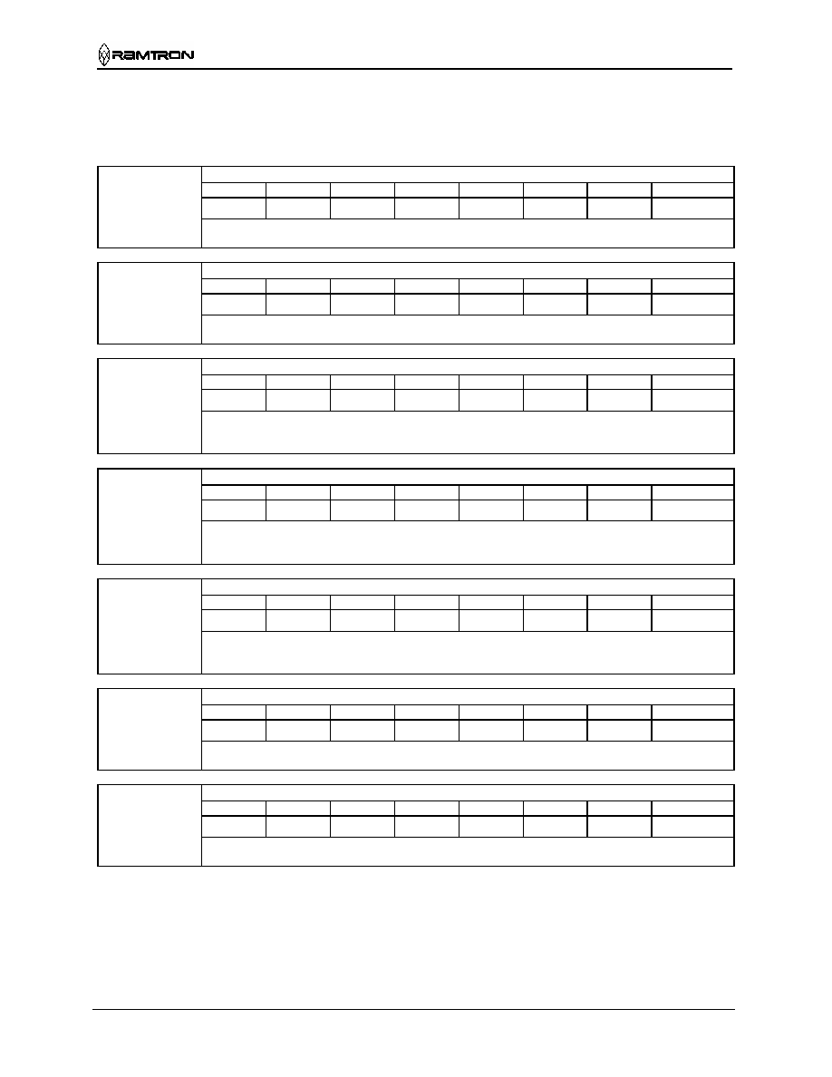
Table 1. Register Map
Address Description
8h
Timekeeping ≠ Years
D7 D6 D5 D4 D3 D2 D1 D0
10 year.3
10 year.2
10 year.1
10 year.0 Year.3 Year.2 Year.1
Year.0
Contains the lower two BCD digits of the year. Lower nibble contains the value for years; upper nibble
contains the value for 10s of years. Each nibble operates from 0 to 9. The range for the register is 0-99.
7h
Timekeeping ≠ Months
D7 D6 D5 D4 D3 D2 D1 D0
0 0 0
10
Month
Month.3
Month.2
Month.1
Month.0
Contains the BCD digits for the month. Lower nibble contains the lower digit and operates from 0 to 9;
upper nibble (one bit) contains the upper digit and operates from 0 to 1. The range for the register is 1-12.
6h
Timekeeping ≠ Date of the month
D7 D6 D5 D4 D3 D2 D1 D0
0
0
10 date.1
10 date.0
Date.3
Date.2
Date.1
Date.0
Contains the BCD digits for the date of the month. Lower nibble contains the lower digit and operates
from 0 to 9; upper nibble contains the upper digit and operates from 0 to 3. The range for the register is 1-
31.
5h
Timekeeping ≠ Day of the week
D7 D6 D5 D4 D3 D2 D1 D0
0 0 0 0 0
Day.2
Day.1
Day.0
Lower nibble contains a value that correlates to day of the week. Day of the week is a ring counter that
counts from 1 to 7 then returns to 1. The user must assign meaning to the day value, as the day is not
integrated with the date.
4h
Timekeeping ≠ Hours
D7 D6 D5 D4 D3 D2 D1 D0
0
0
10 hours.1
10 hours.0
Hours.3
Hours2
Hours.1
Hours.0
Contains the BCD value of hours in 24-hour format. Lower nibble contains the lower digit and operates
from 0 to 9; upper nibble (two bits) contains the upper digit and operates from 0 to 2. The range for the
register is 0-23.
3h
Timekeeping ≠ Minutes
D7 D6 D5 D4 D3 D2 D1 D0
0
10 min.2
10 min.1
10 min.0
Min.3
Min.2
Min.1
Min.0
Contains the BCD value of minutes. Lower nibble contains the lower digit and operates from 0 to 9;
upper nibble contains the upper minutes digit and operates from 0 to 5. The range for the register is 0-59.
2h
Timekeeping ≠ Seconds
D7 D6 D5 D4 D3 D2 D1 D0
0
10 sec.2
10 sec.1
10 sec.0
Seconds.3
Seconds.2
Seconds.1
Seconds.0
Contains the BCD value of seconds. Lower nibble contains the lower digit and operates from 0 to 9;
upper nibble contains the upper digit and operates from 0 to 5. The range for the register is 0-59.
FM30C256
Rev 2.1
Dec. 2002
Page 5 of 18
Address Description
1h
CAL/Control
D7 D6 D5 D4 D3 D2 D1 D0
OSCEN TSEN CALS CAL.4 CAL.3 CAL.2 CAL.1 CAL.0
/OSCEN
/Oscillator Enable. When set to 1, the oscillator is halted. When set to 0, the oscillator runs. Disabling
the oscillator can save battery power during storage. On a power-up without battery, this bit is set to 1.
TSEN
Time Stamp Enable. When set to 1, a Tamper Detect event will record the date and time of the event.
On a power-up without battery, this bit is set to 0.
CALS
Calibration sign. Determines if the calibration adjustment is applied as an addition to or as a subtraction
from the time-base. Calibration is explained below.
CAL.4-0
These five bits control the calibration of the clock.
0h
Flags/Control
D7 D6 D5 D4 D3 D2 D1 D0
Tamper CF Reserved
Reserved
TST CAL W
R
Tamper
Tamper Detect. This bit is set to 1 when rising edge is detected on the TIN pin. It can only be cleared to
0 by the user.
CF
Century Overflow Flag. This bit is set to a 1 when the values in the years register overflows from 99 to
00. This indicates a new century, such as going from 1999 to 2000 or 2099 to 2100. The user should
record the new century information as needed. This bit is cleared to 0 when the Flag register is read. It is
read-only for the user.
TST
Invokes factory test mode. Users should always set this bit to 0.
CAL
Calibration Mode. When set to 1, the clock enters calibration mode. When CAL is set to 0, the clock
operates normally, and the CAL pin is driven low.
W
Write Time. Setting the W bit to 1 freezes updates of the timekeeping registers. The user can then write
them with updated values. Setting the W bit to 0 causes the contents of the time registers to be
transferred to the timekeeping counters.
R
Read Time. Setting the R bit to 1 copies a static image of the timekeeping registers and places them in a
holding register. The user can then read them without concerns over changing values causing system
errors. The R bit going from 0 to 1 causes the timekeeping capture, so the bit must be returned to 0 prior
to reading again.
Reserved
Reserved bits. Do not use. Should remain set to 0.
Real-time Clock Operation
The real-time clock (RTC) consists of an oscillator,
divider, and a register system for accessing the
information. It divides down the 32.768 kHz time-
base and provides a minimum resolution of seconds
(1Hz) to the user. Static registers provide the user
with read/write access to the time values. The
synchronization of these registers with the
timekeeper core is performed using R and W bits in
register 0.
Changing the R bit from 0 to 1 causes a transfer of
the timekeeping information to holding registers that
can be read by the user. If a timekeeper update is
pending when R is set, then the update will be
completed prior to loading the registers. Another
update cannot be performed until the R bit is cleared
to 0.
Setting the W bit to 1 causes the timekeeper to freeze
updates. Clearing it to 0 causes the values in the time
registers to be written into the timekeeper core. Users
should be certain not to load invalid values, such as
FFh, to the timekeeping registers.
Updates to the timekeeping core occur continuously
except when frozen. A diagram of the timekeeping
core follows.
Backup Power
The real-time clock/calendar is intended for
permanently powered operation. When the primary
system power fails, the voltage on the VDD pin will
drop. When VDD is less than the voltage on the
VBAK pin, the clock will switch to the backup power
supply. The clock operates at extremely low current
in order to maximize battery life. However, an
advantage of combining a clock function with FRAM
is that the 256K memory data is not lost regardless of
the backup power source.
FM30C256
Rev 2.1
Dec. 2002
Page 6 of 18
32.768 kHz
crystal
Oscillator
Clock
Divider
Update
Logic
512 Hz
W
R
Seconds
7 bits
Minutes
7 bits
Hours
6 bits
Date
6 bits
Months
5 bits
Years
8 bits
CF
Days
3 bits
User Interface Registers
1 Hz
Figure 2. Real-time Clock Core Block Diagram
Calibration
When the CAL bit in register 0 is set to 1, the clock
enters calibration mode. Calibration operates by
applying a digital correction to the counter based on
the frequency error. In CAL mode, the CAL pin is
driven with a 512 Hz (nominal) square wave. Any
measured deviation from 512 Hz is converted to an
error in ppm. This error corresponds to a correction
value that is then written by the user into the
calibration register. The correction factors are listed
in the table below.
Positive ppm errors require a negative adjustment
that removes pulses. Negative ppm errors require a
positive correction that adds pulses. Positive ppm
adjustments have the CALS bit set to 1, where as
negative ppm adjustments have CALS = 0. After
calibration, the clock will have a maximum error of
±
2.17 ppm or
±
0.09 minutes per month at the
calibrated temperature.
The calibration setting is battery backed and is stored
in bits CAL.4-0. This value only can be written when
the CAL bit is set to a 1. To exit the calibration
mode, the user must clear the CAL bit to a 0. When
the CAL bit is 0, the CAL pin will be driven low.
When the calibration mode is entered, the user can
measure the frequency error on the CAL pin. This
error expressed in ppm translates directly into
timekeeping error. An offsetting calibration
adjustment corrects this error. However, the
correction is applied by adding or removing pulses on
a periodic basis. Therefore, the correction will not
appear on the 512 Hz output. The calibration
correction must be applied using the lookup table
below. The timekeeping accuracy can be verified by
comparing the FM30C256 time to a reference source.
FM30C256
Rev 2.1
Dec. 2002
Page 7 of 18
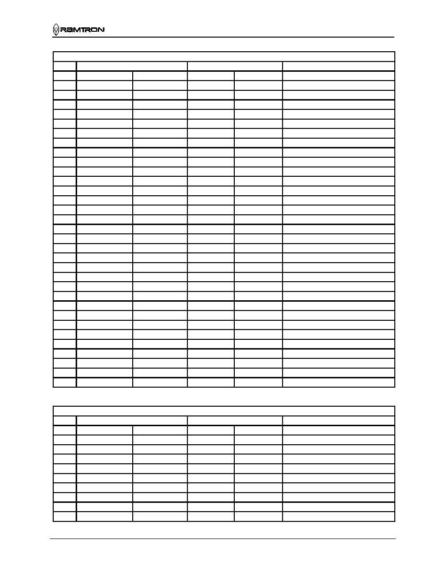
Table 2. Calibration Adjustments
Measured Frequency Range
Error Range (PPM)
Min
Max
Min
Max
Program Calibration Register to:
0
512.0000
511.9989
0
2.17
000000
1
511.9989
511.9967
2.18
6.51
100001
2
511.9967
511.9944
6.52
10.85
100010
3
511.9944
511.9922
10.86
15.19
100011
4
511.9922
511.9900
15.20
19.53
100100
5
511.9900
511.9878
19.54
23.87
100101
6
511.9878
511.9856
23.88
28.21
100110
7
511.9856
511.9833
28.22
32.55
100111
8
511.9833
511.9811
32.56
36.89
101000
9
511.9811
511.9789
36.90
41.23
101001
10
511.9789
511.9767
41.24
45.57
101010
11
511.9767
511.9744
45.58
49.91
101011
12
511.9744
511.9722
49.92
54.25
101100
13
511.9722
511.9700
54.26
58.59
101101
14
511.9700
511.9678
58.60
62.93
101110
15
511.9678
511.9656
62.94
67.27
101111
16
511.9656
511.9633
67.28
71.61
110000
17
511.9633
511.9611
71.62
75.95
110001
18
511.9611
511.9589
75.96
80.29
110010
19
511.9589
511.9567
80.30
84.63
110011
20
511.9567
511.9544
84.64
88.97
110100
21
511.9544
511.9522
88.98
93.31
110101
22
511.9522
511.9500
93.32
97.65
110110
23
511.9500
511.9478
97.66
101.99
110111
24
511.9478
511.9456
102.00
106.33
111000
25
511.9456
511.9433
106.34
110.67
111001
26
511.9433
511.9411
110.68
115.01
111010
27
511.9411
511.9389
115.02
119.35
111011
28
511.9389
511.9367
119.36
123.69
111100
29
511.9367
511.9344
123.70
128.03
111101
30
511.9344
511.9322
128.04
132.37
111110
31
511.9322
511.9300
132.38
136.71
111111
Measured Frequency Range
Error Range (PPM)
Min
Max
Min
Max
Program Calibration Register to:
0
512.0000
512.0011
0
2.17
000000
1
512.0011
512.0033
2.18
6.51
000001
2
512.0033
512.0056
6.52
10.85
000010
3
512.0056
512.0078
10.86
15.19
000011
4
512.0078
512.0100
15.20
19.53
000100
5
512.0100
512.0122
19.54
23.87
000101
6
512.0122
512.0144
23.88
28.21
000110
7
512.0144
512.0167
28.22
32.55
000111
8
512.0167
512.0189
32.56
36.89
001000
Positive Calibration for slow clocks: Calibration will achieve +/- 2.17 PPM after calibration
Negative Calibration for fast clocks: Calibration will achieve +/- 2.17 PPM after calibration
FM30C256
Rev 2.1
Dec. 2002
Page 8 of 18
Tamper Detection and Time Stamp
The TIN pin is a battery-backed input that is used to
detect a tamper event in the system. When a rising
edge occurs on TIN, this Tamper Detect event is
recorded in the MSB of register 0. This action will
occur only when either V
BAK
or V
DD
is applied. Any
further activity on TIN, such as a falling edge, will be
ignored. The user is responsible for reading and
clearing the Tamper flag. Clearing the Tamper flag
allows the TIN to detect another rising edge. The
tamper flag can only be read or cleared when V
DD
4.5V. On a power-up without battery, this bit is set to
zero.
The tamper input TIN can be used to timestamp the
exact time a tamper event occurs. This feature can be
enabled by setting the timestamp enable bit TSEN in
the calibration control register (RTC address 1, bit
D6). At power-up, TSEN is cleared and must be set
by the user. When a rising edge occurs on TIN and
the TSEN bit is set, the date and time of the event
will be recorded. The current time is loaded into the
timekeeping registers. When the system is checked
for a tamper event, the time of the event can be read.
After a tamper event, the timekeeping registers can
be overwritten if the R bit is set before reading the
timekeeping registers. To prevent overwriting the
timestamp, the control register should be read first to
check that the tamper bit is set. If it is set, the
timekeeping registers should be read to collect the
time of the last tamper event. Checking for a tamper
event before setting the R bit will ensure accurate
tamper timestamp information. If the TSEN bit is
not set, then a rising edge on TIN will not trigger a
timestamp.
System Reset Control
The /RST pin allows the user to easily control a
system level reset function. It is an open drain
output and requires an external pullup resistor to
V
DD
for proper operation. When V
DD
is within the
specified operating range, /RST output is tri-stated
and pulled to V
DD
by the external resistor. If V
DD
drops below the reset trip point voltage level (V
TP
)
and remains below this level for the V
TP
noise
immunity duration (t
RNR
), the /RST pin will be
driven low. It will continue to drive low until V
DD
falls below the V
RST
level. When V
DD
rises again
above V
TP
, /RST will continue to drive low for a
duration (t
RPU
) to ensure a robust system reset at a
reliable V
DD
level. After t
RPU
has been met, the /RST
pin tri-states and is pulled high by the external
pullup resistor. Refer to the figure on page 16 for a
graphical description of the /RST function and
timing.
9
512.0189
512.0211
36.90
41.23
001001
10
512.0211
512.0233
41.24
45.57
001010
11
512.0233
512.0256
45.58
49.91
001011
12
512.0256
512.0278
49.92
54.25
001100
13
512.0278
512.0300
54.26
58.59
001101
14
512.0300
512.0322
58.60
62.93
001110
15
512.0322
512.0344
62.94
67.27
001111
16
512.0344
512.0367
67.28
71.61
010000
17
512.0367
512.0389
71.62
75.95
010001
18
512.0389
512.0411
75.96
80.29
010010
19
512.0411
512.0433
80.30
84.63
010011
20
512.0433
512.0456
84.64
88.97
010100
21
512.0456
512.0478
88.98
93.31
010101
22
512.0478
512.0500
93.32
97.65
010110
23
512.0500
512.0522
97.66
101.99
010111
24
512.0522
512.0544
102.00
106.33
011000
25
512.0544
512.0567
106.34
110.67
011001
26
512.0567
512.0589
110.68
115.01
011010
27
512.0589
512.0611
115.02
119.35
011011
28
512.0611
512.0633
119.36
123.69
011100
29
512.0633
512.0656
123.70
128.03
011101
30
512.0656
512.0678
128.04
132.37
011110
31
512.0678
512.0700
132.38
136.71
011111
FM30C256
Rev 2.1
Dec. 2002
Page 9 of 18
Two-wire Interface
The FM30C256 employs an industry standard two-
wire bus that is familiar to many users and for
convenience is described in this section.
The FM30C256 is unique since it incorporates two
logical devices in one chip. Each logical device can
be accessed individually. One is a memory device. It
has a Slave Address (Slave ID = 1010b) that
operates the same as a stand-alone memory device.
The second device is a real-time clock and tamper
detect which share a unique Slave Address (Slave
ID = 1101b).
By convention, any device that is sending data onto
the bus is the transmitter while the target device for
this data is the receiver. The device that is controlling
the bus is the master. The master is responsible for
generating the clock signal for all operations. Any
device on the bus that is being controlled is a slave.
The FM30C256 is always a slave device.
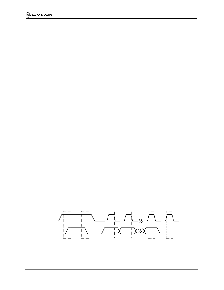
The bus protocol is controlled by transition states in
the SDA and SCL signals. There are four conditions:
Start, Stop, Data bit, and Acknowledge. Figure 4
illustrates the signal conditions that specify the four
states. Detailed timing diagrams are shown in the
electrical specifications.
Start Condition
A Start condition is indicated when the bus master
drives SDA from high to low while the SCL signal is
high. All read and write transactions begin with a
Start condition. An operation in progress can be
aborted by asserting a Start condition at any time.
Aborting an operation using the Start condition will
ready the FM30C256 for a new operation.
If the power supply drops below the specified VDD
minimum during operation, the system should issue a
Start condition prior to performing another operation.
Stop Condition
A Stop condition is indicated when the bus master
drives SDA from low to high while the SCL signal
is high. All operations must end with a Stop
condition. If an operation is pending when a stop is
asserted, the operation will be aborted. The master
must have control of SDA (not a memory read) in
order to assert a Stop condition.
Data/Address Transfer
All data transfers (including addresses) take place
while the SCL signal is high. Except under the two
conditions described above, the SDA signal should
not change while SCL is high.
Acknowledge
The Acknowledge takes place after the 8
th
data bit
has been transferred in any transaction. During this
state the transmitter must release the SDA bus to
allow the receiver to drive it. The receiver drives the
SDA signal low to acknowledge receipt of the byte.
If the receiver does not drive SDA low, the
condition is a No-Acknowledge and the operation is
aborted.
The receiver might fail to acknowledge for two
distinct reasons. First is that a byte transfer fails. In
this case, the No-Acknowledge ends the current
operation so that the part can be addressed again.
This allows the last byte to be recovered in the event
of a communication error.
Second and most common, the receiver does not
send an Acknowledge to deliberately terminate an
operation. For example, during a read operation, the
FM30C256 will continue to place data onto the bus
as long as the receiver sends Acknowledges (and
clocks). When a read operation is complete and no
more data is needed, the receiver must not
acknowledge the last byte. If the receiver
acknowledges the last byte, this will cause the
FM30C256 to attempt to drive the bus on the next
clock while the master is sending a new command
such as a Stop.
Stop
(Master)
Start
(Master)
7
Data bits
(Transmitter)
6
0
Data bit
(Transmitter)
Acknowledge
(Receiver)
SCL
SDA
Figure 3. Data Transfer Protocol
FM30C256
Rev 2.1
Dec. 2002
Page 10 of 18
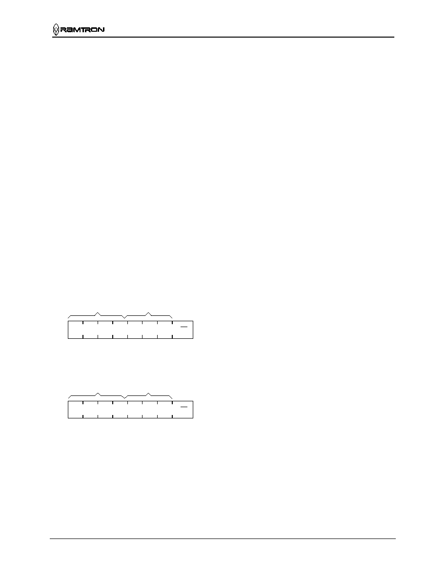
Slave Address
The first byte that the FM30C256 expects after a
Start condition is the slave address. As shown in
Figure 4, the slave address contains the Slave ID,
Device Select address, and a bit that specifies if the
transaction is a read or a write.
The FM30C256 has two Slave Addresses (Slave
IDs) associated with two logical devices. To access
the memory device, bits 7-4 should be set to 1010b.
See Figure 4. The other logical device within the
FM30C256 is the real-time clock and tamper detect.
To access this device, bits 7-4 of the slave address
should be set to 1101b. A bus transaction with this
slave address will not affect the memory in any way.
See Figure 5.
The Slave ID bits allow other function types to
reside on the 2-wire bus for a given device select
address. The device select bits (bits 3-1) are used to
select one of eight chips on a two-wire bus. They
must match the corresponding value on the external
address pins in order to select the device. Up to eight
devices can reside on the same two-wire bus by
assigning a different address to each device. Bit 0 is
the read/write bit. A "1" indicates a read operation,
and a "0" indicates a write operation.
1
0
1
0
R/W
Slave
ID
7
6
5
4
3
2
1
0
Device
Select
A2 A1 A0
Figure 4. Slave Address - Memory
1
1
0
1
R/W
Slave
ID
7
6
5
4
3
2
1
0
Device
Select
A2 A1 A0
Figure 5. Slave Address ≠ RTC
Addressing Overview ≠ Memory
After the FM30C256 acknowledges the Slave
Address, the master can place the memory address
on the bus for a write operation. The address requires
two bytes. The first is the MSB (upper byte). Since
the device uses only 15 address bits, the value of the
upper bit is a "don't care". Following the MSB is the
LSB (lower byte) which contains the remaining eight
address bits. The address is latched internally. Each
access causes the latched address to be incremented
automatically. The current address is the value that is
held in the latch, either a newly written value or the
address following the last access. The current
address will be held as long as power remains or
until a new value is written. Accesses to the clock do
not affect the current memory address. Reads always
use the current address. A random read address can
be loaded by beginning a write operation as
explained below.
After transmission of each data byte, just prior to the
Acknowledge, the FM30C256 increments the
internal address. This allows the next sequential byte
to be accessed with no additional addressing
externally. After the last address (7FFFh) is reached,
the address latch will roll over to 0000h. There is no
limit to the number of bytes that can be accessed
with a single read or write operation.
Addressing Overview ≠ RTC
The RTC operates in a similar manner to the
memory, except that it uses only one byte of address.
The low four bits of address specify register 0-8, and
the upper four bits are "don't care". Only addresses
0 through 8 should be loaded during an RTC write
command. Loading addresses 9-F is an illegal
condition and should not be attempted since
unpredictable results could occur.
Data Transfer
After the address information has been transmitted,
data transfer between the bus master and the
FM30C256 begins. For a read, the FM30C256 will
place 8 data bits on the bus then wait for an
Acknowledge from the master. If the Acknowledge
occurs, the FM30C256 will transfer the next byte. If
the Acknowledge is not sent, the FM30C256 will
end the read operation. For a write operation, the
FM30C256 will accept 8 data bits from the master
then send an Acknowledge. All data transfer occurs
MSB (most significant bit) first.
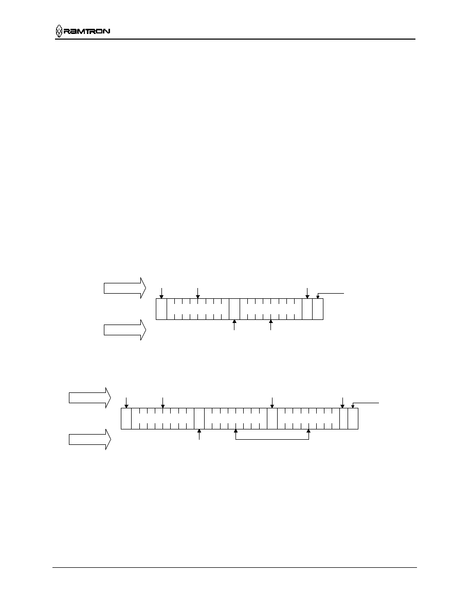
Memory Write Operation
All memory writes begin with a Slave Address, then
a memory address. The bus master indicates a write
operation by setting the slave address LSB to a 0.
After addressing, the bus master sends each byte of
data to the memory and the memory generates an
Acknowledge condition. Any number of sequential
bytes may be written. If the end of the address range
is reached internally, the address counter will wrap
from 7FFFh to 0000h. Internally, the actual memory
write occurs after the 8
th
data bit is transferred. It will

FM30C256
Rev 2.1
Dec. 2002
Page 11 of 18
be complete before the Acknowledge is sent.
Therefore, if the user desires to abort a write without
altering the memory contents, this should be done
using a Start or Stop condition prior to the 8
th
data
bit. Figures 6 and 7 illustrate a single- and multiple-
writes to memory.
S
A
Slave Address
0
Address MSB
A
Data Byte
A
P
By Master
By FM30C256
Start
Address & Data
Stop
Acknowledge
Address LSB
A
Figure 6. Single Byte Memory Write
S
A
Slave Address
0
Address MSB
A
Data Byte
A
P
By Master
By FM30C256
Start
Address & Data
Stop
Acknowledge
Address LSB
A
Data Byte
A
Figure 7. Multiple Byte Memory Write
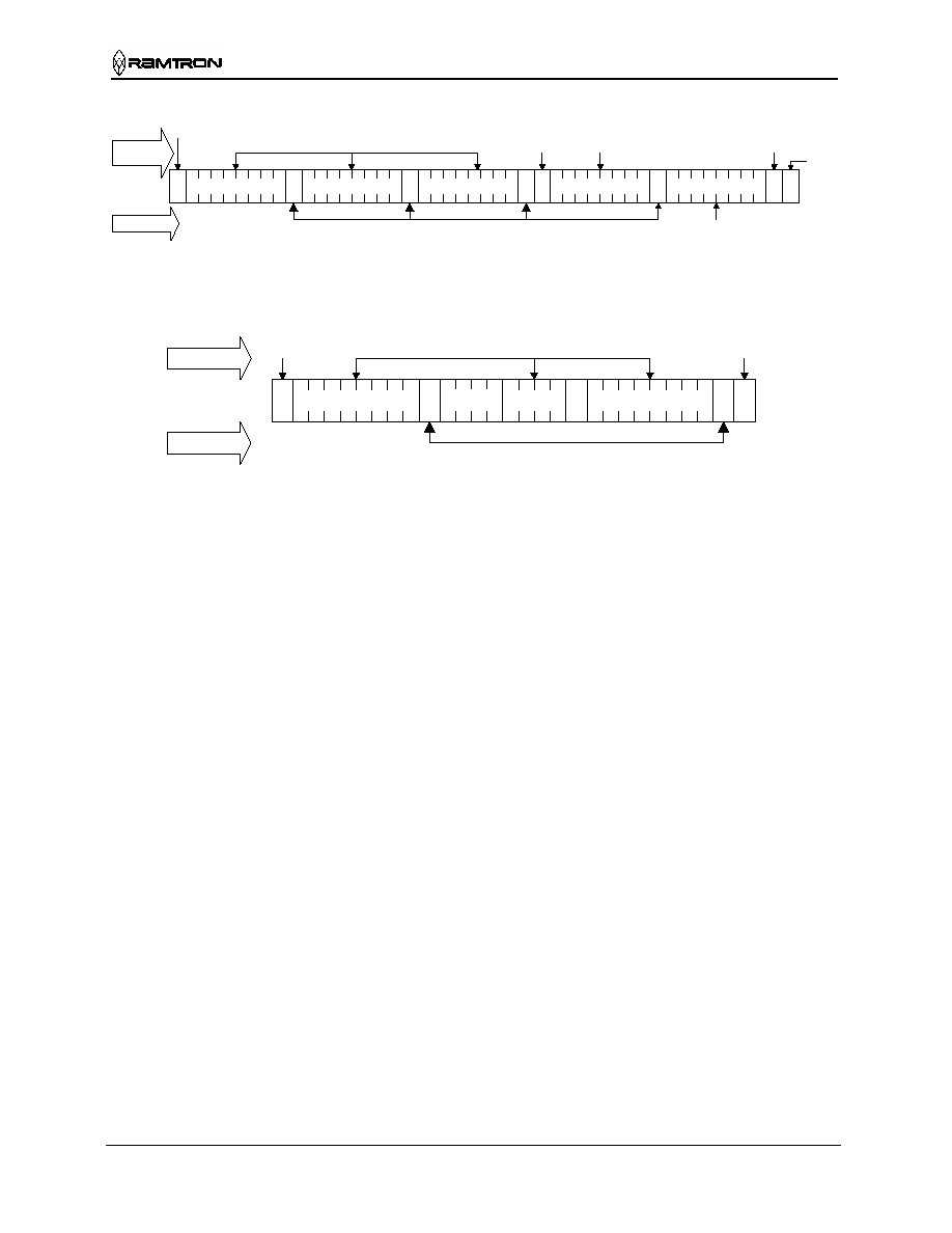
Memory Read Operation
There are two types of memory read operations. They
are current address read and selective address read. In
a current address read, the FM30C256 uses the
internal address latch to supply the address. In a
selective read, the user performs a procedure to set
the address to a specific value.
Current Address & Sequential Read
As mentioned above the FM30C256 uses an internal
latch to supply the address for a read operation. A
current address read uses the existing value in the
address latch as a starting place for the read
operation. The system reads from the address
immediately following that of the last operation.
To perform a current address read, the bus master
supplies a slave address with the LSB set to 1. This
indicates that a read operation is requested. After
receiving the complete device address, the
FM30C256 will begin shifting data out from the
current address on the next clock. The current address
is the value held in the internal address latch.
Beginning with the current address, the bus master
can read any number of bytes. Thus, a sequential read
is simply a current address read with multiple byte
transfers. After each byte the internal address counter
will be incremented.
Each time the bus master acknowledges a byte,
this indicates that the FM30C256 should read
out the next sequential byte.
There are four ways to terminate a read operation.
Failing to properly terminate the read will most likely
create a bus contention as the FM30C256 attempts to
read out additional data onto the bus. The four valid
methods follow.
1. The bus master issues a No-Acknowledge in the
9
th
clock cycle and a Stop in the 10
th
clock cycle.
This is illustrated in the diagrams below. This is
preferred.
2. The bus master issues a No-Acknowledge in the
9
th
clock cycle and a start in the 10
th
.
3. The bus master issues a Stop in the 9
th
clock
cycle.
4. The bus master issues a Start in the 9
th
clock
cycle.
If the internal address reaches 7FFFh, it will wrap
around to 0000h on the next read cycle. Figures 8 and
9 show the proper operation for current address reads.
Selective (Random) Read
There is a simple technique that allows a user to
select a random address location as the starting point
for a read operation. This involves using the first
FM30C256
Rev 2.1
Dec. 2002
Page 12 of 18
three bytes of a write operation to set the internal
address followed by subsequent read operations.
To perform a selective read, the bus master sends out
the slave address with the LSB set to 0. This specifies
a write operation. According to the write protocol,
the bus master then sends the address bytes that are
loaded into the internal address latch. After the
FM30C256 acknowledges the address, the bus master
issues a Start condition. This simultaneously aborts
the write operation and allows the read command to
be issued with the slave address LSB set to a 1. The
operation is now a read from the current address.
Figure 10 shows the proper operation for a selective
read.
RTC Write Operation
All RTC writes operate in a similar manner to
memory writes. The distinction is that a different
device ID is used and only one byte address is needed
instead of two. Figure 11 illustrates a single byte
write to the clock.
RTC Read Operation
As with writes, a read operation begins with the
Slave Address. To perform a register read, the bus
master supplies a Slave Address with the LSB set to
1. This indicates that a read operation is requested.
After receiving the complete Slave Address, the
FM30C256 will begin shifting data out from the
current register address on the next clock. Auto-
increment operates for the RTC address as with the
memory address. A current address read for the RTC
looks exactly like the memory except that the device
ID is different. The FM30C256 contains two separate
address registers, one for the 256K memory address
and the other for the RTC register address. This
allows the contents of one address register to be
modified without affecting the current address of the
other register. For example, this would allow an
interrupted read to the memory while still providing
fast access to an RTC register. A subsequent memory
read will then continue from the memory address
where it previously left off, without requiring the
load of a new memory address. However, a write
sequence always requires an address to be supplied.
S
A
Slave Address
1
Data Byte
1
P
By Master
By FM30C256
Start
Address
Stop
Acknowledge
No
Acknowledge
Data
Figure 8. Current Address Memory Read
S
A
Slave Address
1
Data Byte
1 P
By Master
By FM30C256
Start
Address
Stop
Acknowledge
No
Acknowledge
Data
Data Byte
A
Acknowledge
Figure 9. Sequential Memory Read
FM30C256
Rev 2.1
Dec. 2002
Page 13 of 18
S
A
Slave Address
1
Data Byte
1 P
By Master
By FM30C256
Start
Address
Stop
No
Acknowledge
Data
S
A
Slave Address
0
Address MSB
A
Start
Address
Acknowledge
Address LSB
A
Figure 10. Selective (Random) Memory Read
S
A
Slave Address
0
Address
A
Data Byte
A
P
By Master
By FM30C256
Start
Address & Data
Stop
Acknowledge
X X
X
X
Figure 11. Byte RTC Write
FM30C256
Rev 2.1
Dec. 2002
Page 14 of 18
Electrical Specifications
Absolute Maximum Ratings
Symbol Description Ratings
V
DD
Power Supply Voltage with respect to V
SS
-1.0V to +7.0V
V
IN
Voltage on any signal pin with respect to V
SS
-1.0V to +7.0V and
V
IN
< V
DD
+1.0V
T
STG
Storage temperature
-55
∞
C to + 125
∞
C
T
LEAD
Lead temperature (Soldering, 10 seconds)
300
∞
C
Stresses above those listed under Absolute Maximum Ratings may cause permanent damage to the device. This
is a stress rating only, and the functional operation of the device at these or any other conditions above those
listed in the operational section of this specification is not implied. Exposure to absolute maximum ratings
conditions for extended periods may affect device reliability.
DC Operating Conditions
(T
A
= -40
∞
C to + 85
∞
C, V
DD
= 4.5V to 5.5V unless otherwise specified)
Symbol Parameter
Min
Typ
Max
Units
Notes
V
DD
Main Power Supply
4.5
5.0
5.5
V
I
DD
V
DD
Supply Current
@ SCL = 100 kHz
@ SCL = 400 kHz
@ SCL = 1 MHz
300
650
1.35
µ
A
µ
A
mA
1
I
SB
Standby
Current
150
µ
A
2
V
BAK
Clock
Backup
Voltage
2.5
3.0
3.5
V
I
BAK
Clock
Backup
Current
1
µ
A
5
V
TP
V
DD
trip point voltage that activates /RST
4.2
4.5
V
6
V
RST
V
DD
min for Active /RST
@ I
OL
= 80
µ
A, V
OL
= 0.4V
1.2 - V
7
I
LI
Input
Leakage
Current
10
µ
A
3
I
LO
Output
Leakage
Current
10
µ
A
3
V
IL
Input Low Voltage
-0.3
0.3 V
DD
V
V
IH
Input High Voltage
0.7 V
DD
V
DD
+ 0.5
V
V
ILB
Input Low Voltage (TIN)
for V
DD
< V
BAK
-0.3 0.5
V
4
V
IHB
Input High Voltage (TIN)
for V
DD
< V
BAK
V
BAK
≠ 0.5
V
BAK
+ 0.5
V
4
V
OL
Output Low Voltage (CAL, /RST, SDA)
@ I
OL
= 3 mA
0.4
V
V
OH
Output High Voltage (CAL)
@ I
OH
= -2 mA
2.4 V
R
IN
Address Input Resistance (A2-A0)
for V
IN
= V
IL
(max)
for V
IN
= V
IH
(min)
20
1
K
M
V
HYS
Input Hysteresis
0.05 V
DD
V 4
Notes
1.
SCL toggling between V
DD
-0.3V and V
SS
, other inputs V
SS
or V
DD
-0.3V
2.
SCL = SDA = V
DD
. All inputs at V
SS
or V
DD
. Stop command issued.
3.
V
IN
or V
OUT
= V
SS
to V
DD
. Does not apply to pins with internal pull down resistors.
4.
This parameter is characterized but not tested.
5.
V
BAK
= 3.0V, V
DD
< V
BAK
; oscillator running.
6.
/RST is asserted active when V
DD
< V
TP
.
7.
The minimum V
DD
to guarantee the level of /RST remains a valid V
OL
level.
FM30C256
Rev 2.1
Dec. 2002
Page 15 of 18
AC Parameters
(T
A
= -40
∞
C to + 85
∞
C, V
DD
= 4.5V to 5.5V, C
L
= 100 pF unless otherwise specified)
Symbol Parameter
Min Max Min Max Min Max Units Notes
f
SCL
SCL Clock Frequency
0
100
0
400
0
1000
kHz
t
LOW
Clock
Low
Period
4.7 1.3 0.6
µ
s
t
HIGH
Clock
High
Period
4.0 0.6 0.4
µ
s
t
AA
SCL Low to SDA Data Out Valid
3
0.9
0.55
µ
s
t
BUF
Bus Free Before New Transmission
4.7
1.3
0.5
µ
s
t
HD:STA
Start Condition Hold Time
4.0
0.6
0.25
µ
s
t
SU:STA
Start Condition Setup for Repeated
Start
4.7 0.6 0.25
µ
s
t
HD:DAT
Data
In
Hold
0 0 0 ns
t
SU:DAT
Data
In
Setup
250 100 100 ns
t
R
Input Rise Time
1000
300
300
ns
1
t
F
Input
Fall
Time
300 300 100 ns 1
t
SU:STO
Stop Condition Setup
4.0
0.6
0.25
µ
s
t
DH
Data Output Hold
(from SCL @ VIL)
0 0 0 ns
t
SP
Noise Suppression Time Constant
on SCL, SDA
50 50 50 ns
Notes: All SCL specifications as well as start and stop conditions apply to both read and write operations.
1
This parameter is periodically sampled and not 100% tested.
Power Cycle Timing
(T
A
= -40
∞
C to + 85
∞
C)
Symbol Parameter Min
Typ
Max
Units
Notes
t
RPU
Reset active after V
DD
>V
TP
100
-
200
ms
t
RNR
V
DD
< V
TP
noise immunity
10
-
25
µ
s
1
t
R
Rise time of V
DD
from V
BAK
to V
TP
100
-
µ
s
1,2
t
F
Fall time of V
DD
from V
TP
to V
BAK
100
-
µ
s
1,2
Notes
1
This parameter is periodically sampled and not 100% tested.
2
Slew rate for proper transition between the battery-backed and normal operation.
Data Retention
(V
DD
= 4.5V to 5.5V unless otherwise specified)
Parameter Min
Units
Notes
Data Retention
10
Years
1
Notes
1.
The relationship between retention, temperature, and the associated reliability level is
characterized separately.
Capacitance
(T
A
= 25
∞
C, f=1.0 MHz, V
DD
= 5V)
Symbol Parameter Max
Units
Notes
C
IO
Input/output
capacitance
(SDA)
8 pF 1
C
I
Input
capacitance
6 pF 1
C
XTAL
X1, X2 Crystal pin capacitance
12
pF
1, 2
Notes
1
This parameter is periodically sampled and not 100% tested.
2
The crystal attached to the X1/X2 pins must be rated as 6pF.

FM30C256
Rev 2.1
Dec. 2002
Page 16 of 18
AC Test Conditions
Equivalent AC Load Circuit
Input Pulse Levels
0.1 V
DD
to 0.9 V
DD
Input rise and fall times
10 ns
Input and output timing levels
0.5 V
DD
Diagram Notes
All start and stop timing parameters apply to both read and write
cycles. Clock specifications are identical for read and write cycles.
Write timing parameters apply to slave address, word address, and
write data bits. Functional relationships are illustrated in the relevant
data sheet sections. These diagrams illustrate the timing parameters
only.
Read Bus Timing
t
SU:SDA
Start
t
R
`
t
F
Stop Start
t
BUF
t
HIGH
1/fSCL
t
LOW
t
SP
t
SP
Acknowledge
t
HD:DAT
t
SU:DAT
t
AA
t
DH
SCL
SDA
Write Bus Timing
t
SU:STO
Start
Stop Start
Acknowledge
t
AA
t
HD:DAT
t
HD:STA
t
SU:DAT
SCL
SDA
/RST Timing
VDD
VTP
VRST
RST
t
RPU
VBAK
t
F
t
R
t
RNR
5.5V
Output
1700
100 pF
FM30C256
Rev 2.1
Dec. 2002
Page 17 of 18
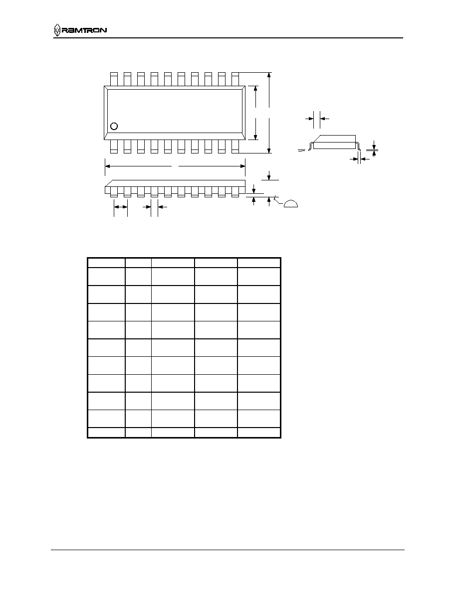
20-pin SOIC (JEDEC Standard MS-013 Variation AC)
Pin 1
E H
D
A1
A
B
e
0.10 mm
0.004 in.
h
45
∞
L
C
Controlling dimensions in millimeters.
Conversions to inches are not necessarily exact.
Symbol Dim
Min
Nom.
Max
A mm
in.
2.35
0.093
2.65
0.104
A1 mm
in.
0.10
0.004
0.30
0.012
B mm
in.
0.33
0.013
0.51
0.020
C mm
in.
0.23
0.009
0.32
0.013
D mm
in.
12.60
0.496
13.00
0.512
E mm
in.
7.40
0.291
7.50
0.295
7.60
0.299
e mm
in.
1.27
BSC
0.050 BSC
H mm
in.
10.00
0.393
10.65
0.419
L mm
in.
0.40
0.016
1.27
0.05
0
∞
8
∞
FM30C256
Rev 2.1
Dec. 2002
Page 18 of 18
Revision History
Revision
Date
Summary
0.1 5/10/01
Initial
Release
0.2
9/17/01
Updated package & pinout. Changed Idd and Capacitance specifications.
CAL pin changed from open drain to push/pull. CAL pin drives low when
CAL bit is reset. TIN pin powered by VBAK, added DC specs for TIN.
Timestamp feature added to Tamper Detect. Changed test load to 1700 ohms
to reflect 3mA V
OL
test condition.
2.0
2/18/02
Changed to production status. Updated package drawing.
2.0A
4/17/02
Increased storage temperature range. Changed V
TP
(max) and I
OL
condition.
2.1
12/16/02
Modified block diagram and pin description to clarify crystal pins X1, X2.