
NOTE : All Specification subject to change without notice
.
49
Electrical Characteristics(23
)
Max Time to Trip
Resistance
Tolerance
Hold
Current
Trip
Current
Rated
Voltage
Max
Current
Typical
Power
Current Time
R
MIN
R1
MAX
Part
Number
I
H
,
A
I
T
,
A
V
MAX
,
Vdc
I
MAX
, A
Pd
,
W
A
Sec
FSMD005-1206
0.05
0.15
60
10
0.4
0.25
1.50
3.60
50.00
FSMD010-1206
0.10
0.25
60
10
0.4
0.50
1.00
1.60
15.00
FSMD020-1206
0.20
0.40
30
10
0.4
8.00
0.05
0.60
2.50
FSMD035-1206
0.35
0.75
16
40
0.4
8.00
0.10
0.30
1.20
FSMD050-1206
0.50
1.00
8
40
0.4
8.00
0.10
0.15
0.70
FSMD075-1206
0.75
1.50
6
40
0.6
8.00
0.20
0.10
0.29
FSMD100-1206
1.00
1.80
6
40
0.6
8.00
0.30
0.055
0.210
FSMD150-1206
1.50
3.00
6
40
0.8
8.00
1.00
0.040
0.120
I
H
=Hold current-maximum current at which the device will not trip at 23
still air.
I
T
=Trip current-minimum current at which the device will always trip at 23
still air.
V
MAX
=Maximum voltage device can withstand without damage at it rated current.(I max)
I
MAX
= Maximum fault current device can withstand without damage at rat ed voltage (V max).
Pd=Typical power dissipated-type amount of power dissipated by the device when in the tripped state in 23
still air environment.
R
MIN
=Minimum device resistance at 23
prior to tripping.
R
1
MAX
=Maximum device resistance at 23
measured 1 hour post trip.
Termination pad characteristics
Termination pad materials : solder-plated copper
Lead Free Component
Application:
All high-density boards
Product Features:
Small surface mount, Solid state
Faster time to trip than standard SMD devices
Lower resistance than standard SMD devices
Operation Current: 50mA~1.5A
Maximum Voltage: 6V~60V
Temperature Range: -40
to 85
Agency Recognition: Pending
FSMD1206 Series
Surface Mount PTC
PDF created with FinePrint pdfFactory trial version
http://www.pdffactory.com
NOTE : All Specification subject to change without notice
.
50
FSMD Product Dimensions (Millimeters)
A
B
C
D
Part
Number
Min
Max
Min
Max
Min
Max
Min
FSMD005-1206
3.0
3.5
1.50
1.80
0.45
0.75
0.10
FSMD010-1206
3.0
3.5
1.50
1.80
0.45
0.75
0.10
FSMD020-1206
3.0
3.5
1.50
1.80
0.45
0.75
0.10
FSMD035-1206
3.0
3.5
1.50
1.80
0.45
0.75
0.10
FSMD050-1206
3.0
3.5
1.50
1.80
0.25
0.55
0.10
FSMD075-1206
3.0
3.5
1.50
1.80
0.45
1.25
0.10
FSMD100-1206
3.0
3.5
1.50
1.80
0.75
1.25
0.10
FSMD150-1206
3.0
3.5
1.50
1.80
0.80
1.80
0.10
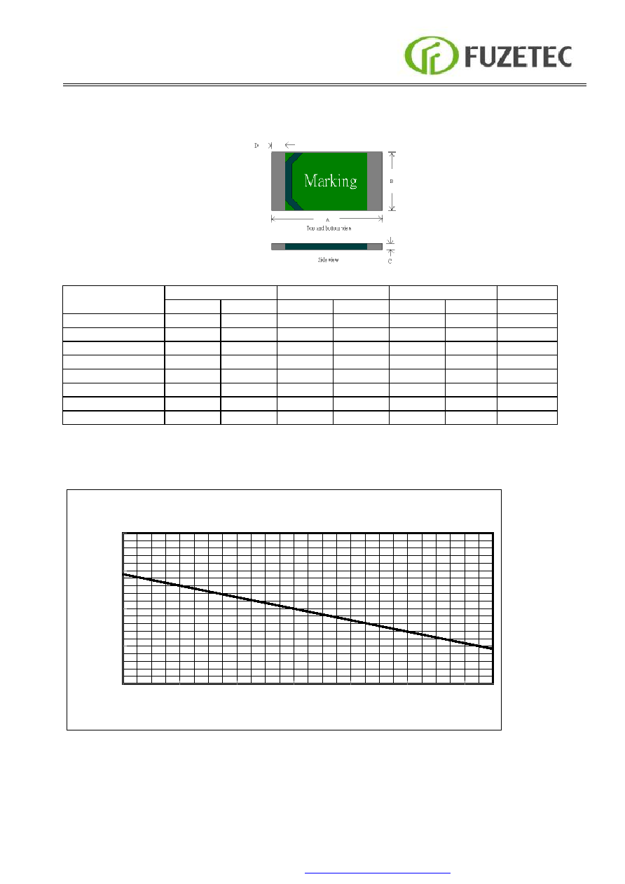
Thermal Derating Curve
Thermal Derating Curve, FSMD1206 Series
0%
50%
100%
150%
200%
-40
-20
0
20
40
60
80
Ambient Temperature (C)
P
e
r
c
e
n
t
o
f
R
a
t
e
d
H
o
l
d
a
n
d
T
r
i
p
C
u
r
r
e
n
t
FSMD1206 Series
Surface Mount PTC
PDF created with FinePrint pdfFactory trial version
http://www.pdffactory.com

NOTE : All Specification subject to change without notice
.
51
F A
Typical Time-To-Trip at 23
A B C D E F G
0.001
0.01
0.1
1
10
100
0.1
1
10
100
Fault current (A)
T
i
m
e
-
t
o
-
t
r
i
p
(
S
)
Part Numbering System
Part Marking System
F S M D
Current rating
Example
Standard Package
Warning: -Operation beyond the specified maximum ratings or improper use may result in damage and possible electrical
arcing and/or flame.
-PPTC device are intended for occasional overcurrent protection. Application for repeated overcurrent condition
and/or prolonged trip are not anticipated.
-Avoid contact of PPTC device with chemical solvent. Prolonged contact will damage the device performance.
P/N
Pcs /Bag Reel/Tape
P/N
Pcs /Bag
Reel/Tape
FSMD005-1206
--------
4K
FSMD050-1206
--------
4K
FSMD010-1206
--------
4K
FSMD075-1206
--------
4K
FSMD020-1206
--------
4K
FSMD100-1206
--------
4K
FSMD035-1206
--------
4K
FSMD150-1206
--------
4K
Z =FSMD005-1206
A =FSMD010-1206
B =FSMD020-1206
C =FSMD035-1206
D =FSMD050-1206
E =FSMD075-1206
F =FSMD100-1206
G =FSMD150-1206
F
Part Identification
Fuzetec Logo
FZ =FSMD005-1206
FA =FSMD010-1206
FB =FSMD020-1206
FC =FSMD035-1206
FD =FSMD050-1206
FE =FSMD075-1206
FF =FSMD100-1206
FG=FSMD150-1206
Z
FSMD1206 Series
Surface Mount PTC
PDF created with FinePrint pdfFactory trial version
http://www.pdffactory.com

NOTE : All Specification subject to change without notice
.
52
Pad Layouts
Solder Reflow and Rework Recommendations
The dimension in the table below provide the recommended pad layout for each FSMD1206 device
Pad dimensions(millimeters)
Device
A
Nominal
B
Nominal
C
Nominal
FSMD005-1206
2.00
1.00
1.90
FSMD010-1206
2.00
1.00
1.90
FSMD020-1206
2.00
1.00
1.90
FSMD035-1206
2.00
1.00
1.90
FSMD050-1206
2.00
1.00
1.90
FSMD075-1206
2.00
1.00
1.90
FSMD100-1206
2.00
1.00
1.90
FSMD150-1206
2.00
1.00
1.90
Solder reflow
Due to
"
Lead Free
"
nature, Temperature and
Dwelling time for the soldering zone is higher
than those for Regular. This may cause damage to
other components.
1. Recommended reflow methods; IR , vapor phase oven,
hot air oven.
2. The FSMD1206 Series are suitable for use with
wave-solder application methods.
3. Recommended maximum paste thickness is 0.25mm.
4. Devices can be cleaned using standard industry
methods and solvents.
CAUTION:
If reflow temperatures exceed the recommended
Profile, devices may not meet the performance
requirements.
Rework:
Use standard industry practices.
FSMD1206 Series
Surface Mount PTC
PDF created with FinePrint pdfFactory trial version
http://www.pdffactory.com