
1
GLT41116
64k x 16 CMOS Dynamic RAM with Fast Page Mode
F
EATURES
x
65,536 words by 16 bits organization.
x
Fast access time and cycle time.
x
Dual CAS input.
x
Low power dissipation.
x
Read-Modify-Write, RAS-Only Refresh,
CAS-before-RAS Refresh, Hidden Refresh and Test
Mode Capability.
x
256 refresh cycles per 4ms.
x
Available in 40-Pin 400 mil SOJ, and 40/44-Pin TSOP
(Type II).
x
Single 5.0V
±
10% Power Supply.
x
All inputs and Outputs are TTL compatible.
x
Fast Page Mode operation.
G
ENERAL
D
ESCRIPTION
The GLT41116 is a 65,536 x 16 bit high-performance
CMOS dynamic random access memory. The GLT41116
offers Fast Page mode, and has both BYTE WRITE and
WORD WRITE access cycles via two CAS pins. The
GLT41116 has symmetric address and accepts 256-cycle
refresh in 4ms interval.
All inputs are TTL compatible. Fast Page Mode operation
allows random access up to 256x16 bits, within a page,
with cycle times as short as 18ns.
The GLT41116 is best suited for graphics, and DSP appli-
cations requiring high performance memories.
July 1998 (Rev. 1)
2
G-LINK Technology
GLT41116
July 1998 (Rev. 1)
F
UNCTIONAL
B
LOCK
D
IAGRAM
RAS
LCAS
V
CC
GND
A[7:0]
OE
DQ[7:0]
DQ[15:8]
UCAS
Figure 1. GLT41116 64 x 16 CMOS
WE
Clock Generator
Column
Address Buffer
Row
Address Buffer
Data Output
Buffer
Row Decoder
Lower Byte Control
Memory Array
256 x 256 x 16
Sense Amplifier
Column Decoder
Data Input
Buffer
Data Output
Buffer
Data Input
Buffer
∑∑∑ 256 x 16 ∑∑∑
x 16
x 8
x 8
x 8
x 8
x 8
x 8
x 8
x 8
Y[7:0]
X[7:0]
CAS-before-RAS
Counter
Upper Byte Control
∑∑∑ 256 ∑∑∑
∑∑∑ 256 ∑∑∑
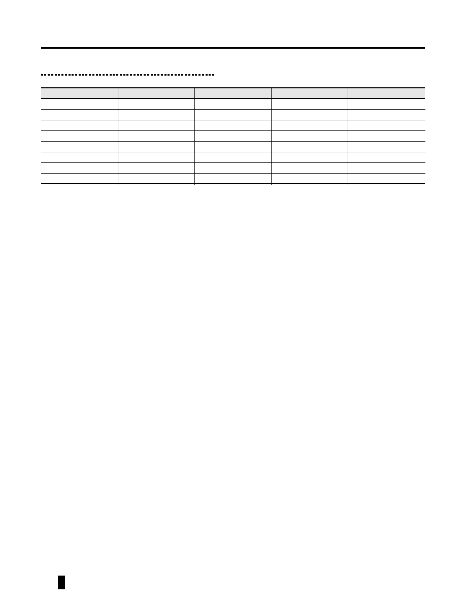
Signal Descriptions
Symbol
Type
Description
A0 - A7
Input
Address Inputs
RAS
Input
Row address strobe
UCAS
Input
Column address strobe/upper byte control
LCAS
Input
Column address strobe/lower byte control
WE
Input
Write enable
OE Input
Output
enable
DQ[15:0]
Input
Data inputs/outputs
V
CC
Input
+5V power supply
V
SS
Input
Ground
NC
Input
No connection
3
G-LINK Technology
GLT41116
July 1998 (Rev. 1)
1. These READ cycles may also be BYTE READ cycles (either UCAS or LCAS active).
2. These WRITE cycles may also be BYTE READ cycles (either UCAS or LCAS active).
3. EARLY WRITE Only.
4. At least one of the two CAS signals must be active (UCAS or LCAS).
Truth Table
Function
Address
RAS
CASL
CASH
WE
OE
DQ
Notes
Stand By
H
H
X
H
X
X
X
High-Z
Read: Word
Row/Col
L
L
L
H
l
Data Out
Read: Lower Byte
Row/Col
L
L
H
H
L
Lower Byte, Data-Out
Upper Byte, High-Z
Read: Upper Byte
Row/Col
L
H
L
H
L
Lower Byte, High-Z
Upper Byte, Data Out
Write: Word (Early Write)
Row/Col
L
L
L
L
X
Data-In
Write: Lower Byte (Early)
Row/Col
L
L
H
L
X
Lower Byte, Data-In
Upper Byte, High-Z
Write: Upper Byte (Early)
Row/Col
L
H
L
L
X
Lower Byte, High-Z
Upper Byte, Data-In
Read Write
Row/Col
L
L
L
H
L
L
H
Data-Out, Data-In
[1]
[2]
Fast-Page Mode Read
1st Cycle
Row/Col
L
H
L
H
L
H
L
Data-Out
[1]
2nd Cycle
Col
L
H
L
H
L
L
X
Data-Out
[1]
Fast-Page Mode Write
1st Cycle
Row/Col
L
H
L
H
L
L
X
Data-In
[2]
2nd Cycle
Col
L
H
L
H
L
L
X
Data-In
[2]
Fast-Page Mode Read-Write
1st Cycle
Row/Col
L
H
L
H
L
H
L
L
H
Data-Out, Data-In
[1]
[2]
2nd Cycle
Col
L
H
L
H
L
H
L
L
H
Data-Out, Data-In
[1]
[2]
Hidden Refresh
Read
Row/Col
L
H
L
L
L
H
L
Data-Out
[1]
Write
Row/Col
L
H
L
L
L
L
X
Data-In
[2]
[3]
RAS-Only Refresh
Row
L
H
H
X
X
High-Z
CBR Refresh
H
L
L
L
X
X
High-Z
[4]

4
G-LINK Technology
GLT41116
July 1998 (Rev. 1)
E
LECTRICAL
S
PECIFICATIONS
1. Stresses greater than those listed under "Absolute Maximum Ratings" may cause permanent damage to the device. This is a stress rating only, and functional operation
of the device at these or any other conditions above those indicated in the operational sections of this specification is not implied. Exposure to absolute maximum rating
conditions for extended periods may affect reliability.
1. Capacitance is sampled and not 100% tested
1. I
CC
is dependent on output loading when the device output is selected. Specified I
CC
(max.) is measured with the output open.
2. I
CC
is dependent upon the number of address transitions specified I
CC
(max) is measured with a maximum of one transition per address cycle in random READ/WRITE and
Fast-Page Mode.
3. Specified V
IL
(min) is steady state operation. During transitions V
IL
(min) may undershoot to -1.0V for a period not to exceed 20 ns. All AC parameter are measured with
V
IL
(min)
VSS and V
IH
(max)
V
CC
.
Absolute Maximum Ratings
[1]
Parameter
Rating
Operating Temperature, T
A
(ambient)
-0
∞
C to +70
∞
C
Storage Temperature (plastic)
-55
∞
C to +125
∞
C
Voltage Relative to V
SS
-1.0V to +7.0V
Short Circuit Output Current`
50 mA
Power Dissipitation
1.0 W
Capacitance
[1]
Symbol
Parameter
Max
Units
C
IN1
Address Input
5
pF
C
IN2
RAS, LCAS, UCAS, WE, OE
7
pF
C
OUT
Data Input/Output
7
pF
DC Characteristics (T
A
= 0
∞
C to 70
∞
C, V
CC
= 5V
±
10%, V
SS
= 0V, unless otherwise specified)
Symbol
Parameter
Conditions
-30
-35
-40
-45
Units
Notes
Min
Max
Min
Max
Min
Max
Min
Max
I
LI
Input Leakage Current
(any input pin)
0V
V
IN
5.5V (All other
pins not under test = 0V)
-10
+10
-10
+10
-10
+10
-10
+10
µ
A
I
LO
Output Leakage Current
(for High-Z State)
0V
V
OUT
5.5V Output is
disabled (Hiz)
+10
+10
+10
+10
µ
A
I
CC1
Operating Current, Ran-
dom READ/WRITE
t
RC
= t
RC
(min.)
180
170
160
150
mA
[1]
[2]
I
CC2
Standby Current, (TTL)
RAS, UCAS, LCAS at V
IH
other inputs
V
SS
2
2
2
2
mA
I
CC3
Refresh Current, RAS-
Only
RAS cycling, UCAS, LCAS at
V
IH
t
RC
= t
RC
(min.)
180
170
160
150
mA
[2]
I
CC4
Operating Current, EDO
Page Mode
RAS at VIL, UCAS, LCAS
address cycling: t
PC
= t
PC
(min.)
180
170
160
150
mA
[1]
[2]
I
CC5
Refresh Current, CAS-
before-RAS
RAS, UCAS, LCAS address
cycling: t
RC
= t
RC
(min.)
180
170
160
150
mA
[1]
I
CC6
Standby Current,
(CMOS)
RAS
V
CC
-0.2V, UCS
V
CC
-0.2V, LCAS
V
CC
-0.2V, All
other inputs
V
CC
2
2
2
2
mA
V
IL
Input Low Voltage
-1
+0.8
-1
+0.8
-1
+0.8
-1
+0.8
V
[3]
V
IH
Input High Voltage
2.4
V
CC
+1
2.4
V
CC
+1
2.4
V
CC
+1
2.4
V
CC
+1
V
V
OL
Output Low Voltage
I
OL
= 4.2 mA
0.4
0.4
0.4
0.4
V
V
OH
Output High Voltage
I
OH
= -5 mA
2.4
2.4
2.4
2.4
V
5
G-LINK Technology
GLT41116
July 1998 (Rev. 1)
AC Characteristics (0
∞
C
T
A
70
∞
C, V
CC
= 5.0V
±
10%)
[1]
[2]
Parameter
Symbol
-30
-35
-40
-45
Units
Notes
Min
Max
Min
Max
Min
Max
Min
Max
Read/Write Cycle Time
t
RC
65
≠
70
≠
75
≠
80
≠
ns
Read Modify Write Cycle Time
t
RWC
80
≠
99
≠
105
≠
110
≠
ns
Access Time for RAS
t
RAC
≠
30
≠
35
≠
40
≠
45
ns
[3]
[4]
Access Time for CAS
t
CAC
≠
10
11
≠
12
≠
≠
12
ns
[3]
[4]
Access TIme from Column Address
t
AA
≠
15
≠
18
≠
20
≠
22
ns
[3]
[4]
CAS to output ion Low-Z
t
CLZ
0
≠
0
≠
0
≠
0
≠
ns
[3]
Output buffer turn-off delay from CAS
t
OFF
3
8
3
8
3
8
3
8
ns
[5]
Transition Time (Rise and Fall)
t
T
3
50
3
50
3
50
3
50
ns
[2]
RAS Precharge Time
t
RP
25
≠
25
≠
25
≠
25
≠
ns
RAS Pulse Width
t
RAS
30
100k
35
100k
40
100k
45
100k
ns
RAS Hold Time
t
RSH
10
≠
12
≠
12
≠
13
≠
ns
CAS Hold Time
t
CSH
30
≠
36
≠
40
≠
46
≠
ns
CAS Pulse Width
t
CAS
10
10k
12
10k
12
10k
13
10k
ns
RAS to CAS Delay Time
t
RCD
13
20
17
24
18
28
18
33
ns
[4]
RAS to Column Address Delay Time
t
RAD
10
15
12
17
13
20
12
23
ns
[4]
CAS To RAS Precharge Time
t
CPRP
5
≠
5
≠
5
≠
5
≠
ns
[6]
Row Address Setup TIme
t
ASR
0
≠
0
≠
0
≠
0
≠
ns
Row Address Hold Time
t
RAH
6
≠
6
≠
6
≠
6
≠
ns
Column Address Setup Time
t
ASC
26
≠
30
≠
34
≠
39
≠
ns
Column Address Hold Time
t
CAH
15
≠
18
≠
20
≠
23
≠
ns
Column Address Hold Time Referenced to RAS
t
AR
26
≠
30
≠
34
≠
39
≠
ns
Column Address Lead Time Referenced to RAS
t
RAL
15
≠
18
≠
20
≠
23
≠
ns
Read Command Setup Time
t
RCS
0
≠
0
≠
0
≠
0
≠
ns
Read Command Hold Time Referenced to RAS
t
RRH
0
≠
0
≠
0
≠
0
≠
ns
[7]
Read Command Hold Time Referenced to CAS
t
RCH
0
≠
0
≠
0
≠
0
≠
ns
[7]
WE Hold Time Referenced to CAS
t
WCH
6
≠
6
≠
6
≠
6
≠
ns
[8]
Write Command Hold time Referenced to RAS
t
WCR
26
≠
30
≠
34
≠
39
≠
ns
[9]
WE Pulse Width
t
WP
6
≠
6
≠
6
≠
6
≠
ns
[8]
WE Lead Time Referenced to RAS
t
RWL
10
≠
11
≠
12
≠
12
≠
ns
WE Lead Time Referenced to CAS
t
CWL
10
≠
11
≠
12
≠
12
≠
ns
Data-In Setup Time
t
DS
0
≠
0
≠
0
≠
0
≠
ns
[10]
Data-In Hold Time
t
DH
7
≠
6
≠
8
≠
8
≠
ns
[10]
Data Hold Time Referenced to RAS
t
DHR
27
≠
31
≠
36
≠
41
≠
ns
[11]
WE Setup Time
t
WCS
0
≠
0
≠
0
≠
0
≠
ns
[9]
RAS to WE Delay Time
t
RWD
47
≠
58
≠
63
≠
68
≠
ns
[9]
CAS to WE Delay Time
t
CWD
24
≠
29
≠
30
≠
30
≠
ns
[9]
Column Address to WE Delay Time
t
AWD
29
≠
36
≠
38
≠
40
≠
ns
[9]
CAS Setup TIme (CAS Before RAS Refresh)
t
CSR
5
≠
5
≠
5
≠
5
≠
ns
CAS Hold Time (CAS Before RAS Refresh)
t
CHR
10
≠
10
≠
10
≠
10
≠
ns
RAS to CAS Precharge Time
t
RPC
5
≠
5
≠
5
≠
5
≠
ns
CAS Precharge Time (CBR Counter Test Cycle)
t
CPT
20
≠
20
≠
20
≠
20
≠
ns
Access Time From CAS Precharge
t
CPA
≠
18
≠
21
≠
23
≠
25
ns
[3]
Fast Page Mode Read/Write Cycle Time
t
PC
18
≠
21
≠
23
≠
25
≠
ns
6
G-LINK Technology
GLT41116
July 1998 (Rev. 1)
1. An initial pause of 100
µ
s is required after power-up followed by any 8 RAS only Refresh or CAS before RAS Refresh Cycles to initialize the internal circuit.
2. V
IH
(min) and V
IL
(min) are reference levels for measuring timing of input signals. Transition times are measured between V
IH
(min) and V
IL
(max), AC measurements as-
sume t
T
= 3 ns.
3. Measured with an equivalent to 2 TTL loads and 100 pF.
4. For read cycles, the access time is defined as follows:
t
RAD
(max.) and t
RCD
(max.) indicate the points which the access time changes and are not the limits of operation.
5. t
OFF
(max.) and t
OEZ
(max.) define the time at which the output achieves the open circuit condition and are not referenced to V
OH
or V
OL
.
6. t
CRP
(min.) requirement should be applicable for RAS, CAS cycle preceded by any cycles.
7. Either t
RCH
(min.) or t
RRH
(min) must be satisfied for a read cycle.
8. t
WP
(min.) is applicable for late write cycle or read modify write cycle. In early write cycles, t
WCH
(min.) should be satisfied.
9. t
WCS
, t
RWD
, t
CWD
and t
AWD
are non-restrictive operating parameters. They are included in the data sheet as electric characteristics only. If t
WCS
t
WCS
(min.), the cycle
is an early write cycle and the data output will remain high impedance for the duration of the cycle. If t
CWD
t
CWD
(min.), t
RWD
t
RWD
(min.) and t
AWD
t
AWD
(min.),
then the cycle is a read-modify-write cycle and the data output will contain the data read from the selected address. If neither of the above conditions is satisfied, the
condition of the data out is indeterminate.
10. This specification is referenced to CAS falling edge in early write cycles and to WE falling edge in late write orr read modify write cycles.
11. t
AR
, t
WCR
, and t
DHR
are referenced to t
RAD
(max.).
Fast Page Mode Read Modify Write Cycle Time
t
PRWC
48
≠
60
≠
53
≠
65
≠
ns
CAS Precharge Time (Fast Page Mode)
t
CP
6
≠
6
≠
7
≠
7
≠
ns
RAS Pulse Width (Fast PAge Mode)
t
RASP
30
100k
35
100k
40
100k
45
100k
ns
RAS Hold Time From CAS Precharge
t
RHCP
25
≠
25
≠
25
≠
30
≠
ns
Access Time From OE
t
OEA
≠
10
≠
11
≠
12
≠
12
ns
OE to Delay Time
t
OED
8
≠
8
≠
8
≠
8
≠
ns
Output Buffer Turn-off Delay Time From OE
t
OEZ
3
≠
3
8
3
8
3
8
ns
[5]
OE Hold Time
t
OEH
6
≠
6
≠
7
≠
7
≠
ns
WE Hold Time (Hidden Refresh Cycle)
t
WHR
15
≠
15
≠
15
≠
15
ns
Refresh Time (256 Cycles)
t
REF
≠
4
≠
4
≠
4
≠
4
ms
AC Characteristics (0
∞
C
T
A
70
∞
C, V
CC
= 5.0V
±
10%)
[1]
[2]
Parameter
Symbol
-30
-35
-40
-45
Units
Notes
Min
Max
Min
Max
Min
Max
Min
Max
Input Conditions
Access Time
t
RAD
t
RAD
(max.) and t
RCD
t
RCD
(max.)
t
RAC
(Max.)
t
RAD
(max.) < t
RAD
and t
RCD
t
RCD
(max.)
t
AA
(Max.)
t
RCD
(max). < t
RCD
t
CAC
(Max.)
7
G-LINK Technology
GLT41116
July 1998 (Rev. 1)
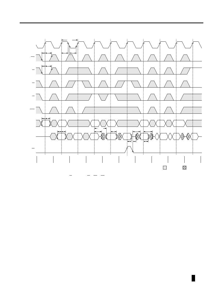
CLK
CKE
CE
R/W
t
KHKL
Figure 2. Read/Write Timing
ADV/LD
BWn
ADDRESS
D/Q
A1
A2
A3
A4
A5
A6
A7
1
2
3
t
KLKH
t
KHKH
4
5
6
7
8
9
10
t
KHEX
t
EVKH
t
KHCX
t
CVKH
t
KHAX
t
AVKH
t
KHDX
t
DVKH
D (A1)
D (A2)
D (A2+1)
Q (A3)
t
KHQV
t
KHQX1
t
KHQX
Q (A4+1)
Q (A4)
D (A5)
D (A6)
D (A7)
OE
t
GHQZ
t
GLQX
t
GLQV
t
KHQZ
t
KHQX
WRITE D(A1)
WRITE D(A2)
BURST WRITE
D(A1+1)
READ Q(A3)
READ Q(A4)
BURST READ
Q(A4+1)
WRITE D(A5)
READ Q(A6)
WRITE D(A7)
DESELECT
NOTE:
1. For this waveform, ZZ is tied LOW.
2. Burst sequence order is determined by MODE (0 = linear, 1 = interleaved). BURST operations are optional.
3. CE represents three signals. When CE = 0, it represents CE = 0, CE2 = 0, CE2 = 1.
4. Data coherency is provided for all possible operations. If a READ is initiated, the most current data is used. The most recent data may be from the input data register.
Don't Care
Undefined
8
G-LINK Technology
GLT41116
July 1998 (Rev. 1)
CLK
CKE
CE
R/Wn
Don't Care
Figure 3. NOP, STALL and DESELECT Timing
ADV/LD
BWn
ADDRESS
D/Q
A1
A2
A3
A4
A5
1
2
3
4
5
6
7
8
9
10
Q (A2)
D (A1)
Undefined
t
KHQZ
t
KHQX
WRITE D(A1)
READ Q(A2)
STALL
READ Q(A1)
WRITE D(A2)
STALL
NOP
READ Q(A3)
DESELECT
Continue
DESELECT
D (A5)
NOTE:
1. The IGNORE CLOCK EDGE or STALL cycle (clock 3) illustrates CKE being used to create a "pause." A WRITE is not performed during this cycle.
2. For this waveform, ZZ and OE are tied LOW.
3. CE represents three signals. When CE = 0, it represents CE = 0, CE2 = 0, CE2 = 1.
4. Data coherency is provided for all possible operations. If a READ is initiated, the most current data is used. The most recent data may be from the input data register.
Q (A3)
D (A4)
9
G-LINK Technology
GLT41116
July 1998 (Rev. 1)
P
ACKAGING
I
NFORMATION
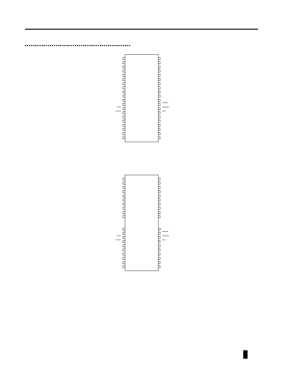
Figure 4. 40-Pin 400 mil Plastic SOJ Pin Assignment
V
CC
DQ0
DQ1
DQ2
DQ3
V
CC
DQ4
DQ5
DQ6
DQ7
NC
NC
WE
RAS
NC
A0
A1
A2
A3
V
CC
V
SS
DQ15
DQ14
DQ13
DQ12
V
SS
DQ11
DQ10
DQ9
DQ8
NC
LCAS
UCAS
OE
NC
A7
A6
A5
A4
V
SS
1
2
3
4
5
6
7
8
9
10
11
12
13
14
15
16
17
18
19
20
40
39
38
37
36
35
34
33
32
31
30
29
28
27
26
25
24
23
22
21
Top View
Figure 5. 44/40-Pin 400 mil TSOP (TypeII) Pin Assignment
V
CC
DQ0
DQ1
DQ2
DQ3
V
CC
DQ4
DQ5
DQ6
DQ7
NC
NC
WE
RAS
NC
A0
A1
A2
V
SS
DQ15
DQ14
DQ13
DQ12
V
SS
DQ11
DQ10
DQ9
DQ8
NC
LCAS
UCAS
OE
NC
A7
A6
A5
1
2
3
4
5
6
7
8
9
10
13
14
15
16
17
18
19
20
44
43
42
41
40
39
38
37
36
35
32
31
30
29
28
27
26
25
Top View
A3
V
CC
A4
V
SS
21
22
24
23
10
G-LINK Technology
GLT41116
July 1998 (Rev. 1)
10.16
±
0.13
11.17
±
0.13
3.6
±
0.25
2.35 TYP
0.65 MIN.
0.2
26.03
±
0.13
SEATING PLANE
0.95 TYP
M
0.18
9.3
±
0.25
Dimensions in millimeters
+0.07
-0.05
1.27
0.81 MAX.
0.43
+0.07
-0.05
1
40
20
21
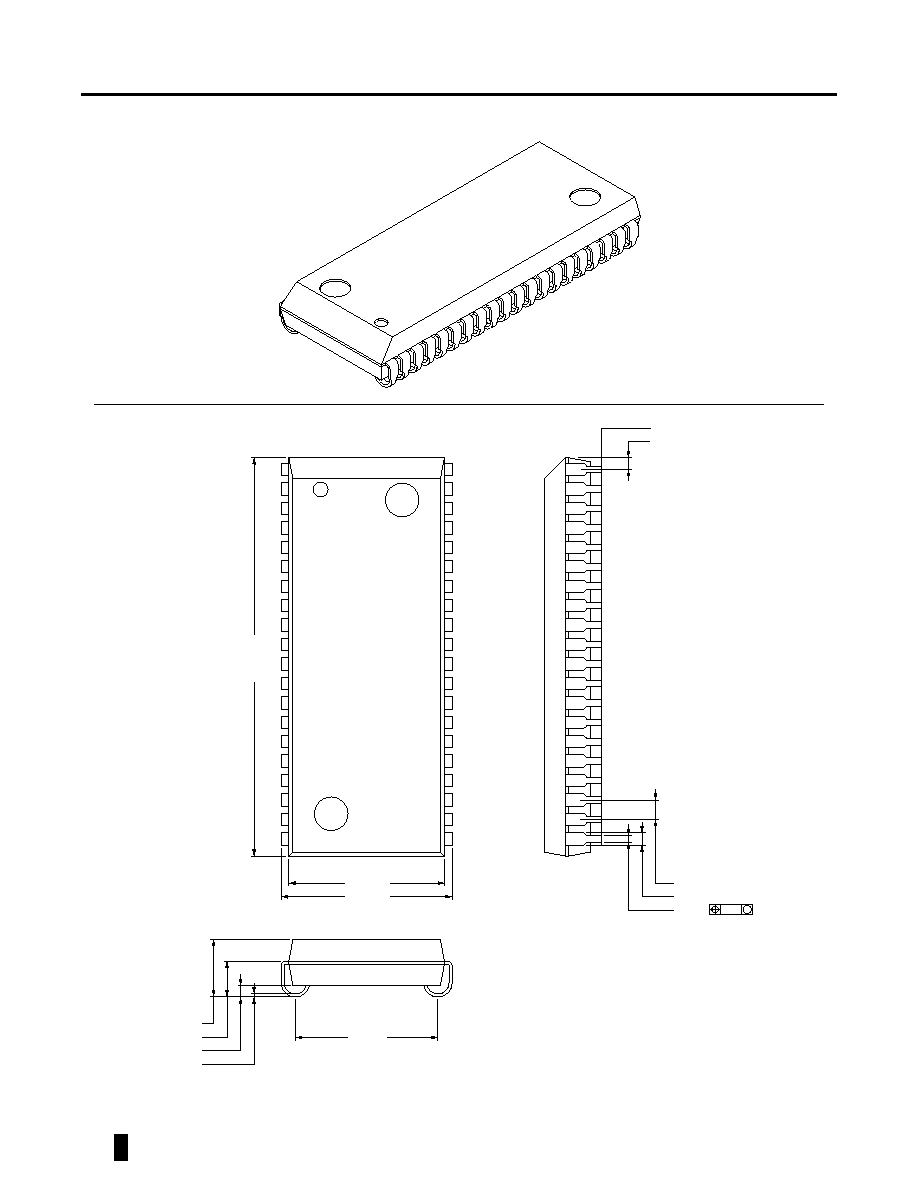
Figure 6. 40-Pin 400 mil SOJ Package Dimensions

11
G-LINK Technology
GLT41116
July 1998 (Rev. 1)
18.41
±
0.1
Dimensions in Inches (millimeters)
Detail A
11.76
±
0.2
10.1
±
0.1
10.76
±
0.2
0.81 TYP
0.8
0.37
SEATING PLANE
A
0.17
±
0.05
1
22
23
44
0.5
±
0.1
0.05 ~ 0.25
0.95
±
0.05
1.2 MAX
0.8
±
0.2
+0.08
-0.07
M
0.16
Figure 7. 40/44-Pin TSOP (Type II) Package Dimensions
12
G-LINK Technology
GLT41116
July 1998 (Rev. 1)
O
RDERING
I
NFO
Part Number
Speed
Power
Feature
Package
GLT4116-30J4
30 ns
Normal
FPM
40-Pin 400 mil SOJ
GLT4116-35J4
35 ns
Normal
FPM
40-Pin 400 mil SOJ
GLT4116-40J4
40 ns
Normal
FPM
40-Pin 400 mil SOJ
GLT4116-45J4
45 ns
Normal
FPM
40-Pin 400 mil SOJ
GLT4116-30TC
30 ns
Normal
FPM
44-Pin 400 mil TSOP
GLT4116-35TC
35 ns
Normal
FPM
44-Pin 400 mil TSOP
GLT4116-40TC
40 ns
Normal
FPM
44-Pin 400 mil TSOP
GLT4116-45TC
45 ns
Normal
FPM
44-Pin 400 mil TSOP

13
G-LINK Technology
GLT41116
July 1998 (Rev. 1)
Notes:

14
G-LINK Technology
GLT41116
July 1998 (Rev. 1)
Notes:

15
G-LINK Technology
GLT41116
July 1998 (Rev. 1)
Notes:
© 2001 G-LINK Technology
All rights reserved. No part of this document may be copied or reproduced in any form or by any means or transferred to any third party without the prior written consent of
G-LINK Technology.
Circuit diagrams utilizing G-LINK products are included as a means of illustrating typical semiconductor applications. Complete information sufficient for design purposes is
not necessarily given.
G-LINK Technology reserves the right to change products or specifications without notice.
The information contained in this document does not convey any license under copyrights, patent rights or trademarks claimed and owned by G-LINK or its subsidiaries.
G-LINK assumes no liability for G-LINK applications assistance, customer's product design, or infringement of patents arising from use of semiconductor devices in such
systems' designs. Nor does G-LINK warrant or represent that any patent right, copyright, or other intellectual property right of G-LINK covering or relating to any combination,
machine, or process in which such semiconductor devices might be or are used.
G-LINK Technology's products are not authorized for use in life support devices or systems. Life support devices or systems are device or systems which are: a) intended for
surgical implant into the human body and b) designed to support or sustain life; and when properly used according to label instructions, can reasonably be expected to cause
significant injury to the user in the event of failure.
The information contained in this document is believed to be entirely accurate. However, G-LINK Technology assumes no responsibility for inaccuracies.
GLT41116
www.glinktech.com
G-LINK Technology
1753 South Main Street
Milpitas, California, 95035, USA
TEL: 408-240-1380 ∑ FAX: 408-240-1385
G-LINK Technology Corporation, Taiwan
6F, No. 24-2, Industry E. Rd. IV
Science-Based Industrial Park
Hsin Chu, Taiwan, R.O.C.
TEL: 03-578-2833 ∑ FAX: 03-578-5820
Printed in USA